EUV Mask Blanks And Methods Of Manufacture
Xiao; Wen ; et al.
U.S. patent application number 16/944556 was filed with the patent office on 2021-02-11 for euv mask blanks and methods of manufacture. This patent application is currently assigned to Applied Materials, Inc., Santa Clara, CA. The applicant listed for this patent is Applied Materials, Inc.. Invention is credited to Vibhu Jindal, Wen Xiao.
| Application Number | 20210041781 16/944556 |
| Document ID | / |
| Family ID | 1000005015202 |
| Filed Date | 2021-02-11 |


| United States Patent Application | 20210041781 |
| Kind Code | A1 |
| Xiao; Wen ; et al. | February 11, 2021 |
EUV Mask Blanks And Methods Of Manufacture
Abstract
An extreme ultraviolet reflective element comprising a multilayer stack of absorber layers on a multilayer stack of reflective layers. The element comprises spacing layer and phase tuning layer. Methods of manufacturing extreme ultraviolet reflective elements and lithography systems including extreme ultraviolet reflective elements are also described.
| Inventors: | Xiao; Wen; (Singapore, SG) ; Jindal; Vibhu; (San Jose, CA) | ||||||||||
| Applicant: |
|
||||||||||
|---|---|---|---|---|---|---|---|---|---|---|---|
| Assignee: | Applied Materials, Inc., Santa
Clara, CA |
||||||||||
| Family ID: | 1000005015202 | ||||||||||
| Appl. No.: | 16/944556 | ||||||||||
| Filed: | July 31, 2020 |
Related U.S. Patent Documents
| Application Number | Filing Date | Patent Number | ||
|---|---|---|---|---|
| 62884396 | Aug 8, 2019 | |||
| Current U.S. Class: | 1/1 |
| Current CPC Class: | G03F 1/24 20130101; G21K 2201/067 20130101; G03F 1/54 20130101; G21K 1/062 20130101 |
| International Class: | G03F 1/24 20060101 G03F001/24; G03F 1/54 20060101 G03F001/54; G21K 1/06 20060101 G21K001/06 |
Claims
1. An extreme ultraviolet (EUV) mask blank comprising: a substrate; a multilayer stack of reflective layers on the substrate, the multilayer stack of reflective layers including a plurality of reflective layer pairs configured to reflect incident light having an intensity I.sub.0 and a phase .PHI..sub.0; a capping layer on the multilayer stack of reflecting layers; a multilayer stack of absorber layers on the capping layer, the multilayer stack of absorber layers including a plurality of absorber layer pairs, each pair comprising a first material A and a second material B, the multilayer stack of absorber layers configured to reflect incident light having an I.sub.1 and a phase .PHI..sub.1; and a spacing layer disposed between the capping layer and the multilayer stack of absorber layers and a phase tuning layer in contact with one of the first material A and the second material B.
2. The extreme ultraviolet (EUV) mask blank of claim 1, wherein the spacing layer has thickness configured to tune intensity of incident light reflected from the multilayer stack of absorber layers (I.sub.1) at a specific wavelength.
3. The extreme ultraviolet (EUV) mask blank of claim 1, the multilayer stack of absorber layers covering a portion of the capping layer such that there is a covered area by the multilayer absorber and an exposed area not covered by multilayer stack of absorber layers, and wherein the phase tuning layer has thickness configured to tune the phase of light reflected from the multilayer stack of reflective layers so that there is a change in phase .DELTA..PHI.=.PHI..sub.1-.PHI..sub.0 that is in a range of from 120.degree. to 240.degree..
4. The extreme ultraviolet (EUV) mask blank of claim 1, wherein the phase tuning layer is on top of the multilayer stack of absorber layers and the spacing layer is directly on the capping layer.
5. The extreme ultraviolet (EUV) mask blank of claim 1, wherein the phase tuning layer is located within the multilayer stack of absorber layers and the spacing layer is directly on the capping layer.
6. The extreme ultraviolet (EUV) mask blank of claim 1, wherein the phase tuning layer is directly on the spacing layer, and the spacing layer is directly on the capping layer.
7. The extreme ultraviolet (EUV) mask blank of claim 1, wherein the spacing layer is directly on the phase tuning layer, and the phase tuning layer is directly on the capping layer.
8. The extreme ultraviolet (EUV) mask blank of claim 1, wherein the reflective layer pairs comprise molybdenum (Mo) and silicon (Si) and the first material A comprises molybdenum (Mo) and the second material B comprises silicon (Si).
9. The extreme ultraviolet (EUV) mask blank of claim 8, wherein the spacing layer comprises a material having an extinction coefficient K less than 0.04 and a material comprising an element selected from the group consisting of Ru, W, Mn, Mo, Nb, Hf, Ti, Zr, Mg, Al, Ge, Se, and Si.
10. The extreme ultraviolet (EUV) mask blank of claim 9, wherein the phase tuning layer comprises a material having an a refraction coefficient n greater than 0.92 and a material comprising an element selected from the group consisting of Cr, Ta, Ti, Fe, Co, Ni, Cu, Zn, Te, Bi, Cd, Ga.
11. A method of manufacturing an extreme ultraviolet (EUV) mask blank, the method comprising: depositing a multilayer stack of reflective layers on a substrate, the multilayer stack of reflective layers including a plurality of reflective layer pairs configured to reflect incident light having an intensity I.sub.0 and a phase .PHI..sub.0; depositing a capping layer on the multilayer stack of reflecting layers; depositing a multilayer stack of absorber layers on the capping layer, the multilayer stack of absorber layers including a plurality of absorber layer pairs, each pair comprising a first material A and a second material B, the multilayer stack of absorber layers configured to reflect incident light having an I.sub.1 and a phase .PHI..sub.1; and forming a spacing layer between the capping layer and the multilayer stack of absorber layers and a phase tuning layer in contact with one of the first material A and the second material B.
12. The method of claim 11, wherein the spacing layer has thickness configured to tune intensity of incident light reflected from the multilayer stack of absorber layers (I.sub.1) at a specific wavelength.
13. The method of claim 11, wherein the multilayer stack of absorber layers covers a portion of the capping layer such that there is a covered area by the multilayer absorber and an exposed area not covered by multilayer stack of absorber layers, and wherein the phase tuning layer has thickness configured to tune the phase of light reflected from the multilayer stack of reflective layers so that there is a change in phase .DELTA..PHI.=.PHI..sub.1-.PHI..sub.0 that is in a range of from 120.degree. to 240.degree..
14. The method of claim 11, wherein the phase tuning layer is deposited on top of the multilayer stack of absorber layers and the spacing layer is deposited directly on the capping layer.
15. The method of claim 11, wherein the phase tuning layer is located within the multilayer stack of absorber layers and the spacing layer is deposited directly on the capping layer.
16. The method of claim 11, wherein the phase tuning layer is deposited directly on the spacing layer, and the spacing layer is deposited directly on the capping layer.
17. The method of claim 11, wherein the spacing layer is deposited directly on the phase tuning layer, and the phase tuning layer is deposited directly on the capping layer.
18. The method of claim 17, wherein the reflective layer pairs comprise molybdenum (Mo) and silicon (Si) and the first material A comprises molybdenum (Mo) and the second material B comprises silicon (Si).
19. The method of claim 18, wherein the spacing layer comprises a material having an extinction coefficient K less than 0.04 and a material comprising an element selected from the group consisting of Ru, W, Mn, Mo, Nb, Hf, Ti, Zr, Mg, Al Ge, Se, and Si and the phase tuning layer comprises a material having an a refraction coefficient n greater than 0.92 and a material comprising an element selected from the group consisting of Cr, Ta, Ti, Fe, Co, Ni, Cu, Zn, Te, Bi, Cd, Ga.
20. An extreme ultraviolet reflective element lithography system comprising: an extreme ultraviolet light source which produces extreme ultraviolet light; a reflective element configured to reflect the extreme ultraviolet light, the reflective element including: a substrate; a multilayer stack of reflective layers on the substrate, the multilayer stack of reflective layers including a plurality of reflective layer pairs configured to reflect incident light having an intensity I.sub.0 and a phase .PHI..sub.0; a capping layer on the multilayer stack of reflecting layers; a multilayer stack of absorber layers on the capping layer, the multilayer stack of absorber layers including a plurality of absorber layer pairs, each pair comprising a first material A and a second material B, the multilayer stack of absorber layers configured to reflect incident light having an I.sub.1 and a phase .PHI..sub.1; and a spacing layer disposed between the capping layer and the multilayer stack of absorber layers and a phase tuning layer in contact with one of the first material A and the second material B.
Description
CROSS-REFERENCE TO RELATED APPLICATIONS
[0001] This application claims priority to U.S. Provisional Application No. 62/884,396, filed Aug. 8, 2019, the entire disclosure of which is hereby incorporated by reference herein.
TECHNICAL FIELD
[0002] The present disclosure relates generally to EUV mask blanks, and more particularly, to EUV mask blanks including spacing and phase tuning layers, and methods of manufacture.
BACKGROUND
[0003] Bragg reflectors are utilized in a wide variety of applications, for example, in EUV mask blanks, optical filters (e.g. band-stop filters, notch filter etc.), fiber Bragg gratings, laser optics, polarizers, and waveguides (e.g. optics for head-mounted displays). Bragg reflectors are typically made of multilayers of alternating thin film materials of different refractive index, wherein high reflectance is one of the key attributes. A Bragg reflector or mirror is a structure formed from a multilayer stack of alternating thin film materials with varying refractive index, for example high- and low-index films. As a result of inter-layer mixing during multilayer depositions, additional interfacial layers form between adjacent layers of different materials. Bragg reflectors must have high reflectance. The structure and properties of the interfacial layers in the multilayer stack play a vital role in the reflectance of Bragg reflectors.
[0004] Extreme ultraviolet (EUV) lithography (EUVL), also known as soft x-ray projection lithography, can be used for the manufacture of 0.0135 micron and smaller minimum feature size semiconductor devices. However, extreme ultraviolet light, which is generally in the 5 to 100 nanometer wavelength range, is strongly absorbed in virtually all materials. For that reason, extreme ultraviolet systems work by reflection rather than by transmission of light. Through the use of a series of mirrors, or lens elements, and a reflective element, or mask blank, coated with a non-reflective absorber mask pattern, the patterned actinic light is reflected onto a resist-coated semiconductor substrate.
[0005] EUVL using a wavelength of 13.53 nm is expected to be a main production process for sub-22 nm half pitch resolution. Mask shadowing is a unique phenomenon caused by use of a multilayer mirror-based mask with an oblique incident angle of light. One method of minimizing the mask shadowing effect is to reduce the absorber thickness. Another approach is a phase shift mask to improve image contrast with a thinner absorber stack. One type of EUV reflective element 100, shown in FIG. 1 is known as an alternating phase shift mask (PSM). The EUV reflective element shown in FIG. 1 includes an EUV phase shift mask (PSM) and comprises an alternating multilayer absorber 115 comprising a first absorber layer 116 of a first material, such as molybdenum, and a second absorber layer 118 of a second material such as silicon disposed on a capping layer 114 of the EUV reflective element 100. The EUV reflective element 100 can be in the form of an EUV mask blank or an extreme ultraviolet mirror. The EUV reflective element 100 includes a substrate 102, a multilayer stack 110 in the form of a Bragg reflector of reflective layers comprising first reflective layer 106, second reflective layer 108, and a capping layer 114. When an EUV reflective element is used in a high numerical aperture (NA) scanner, to optimize imaging resolution of the PSM, intensity (I) and phase (.PHI.) of reflected light from exposed area 100e (I.sub.0 and .PHI..sub.0) shown as line 120 and covered areas 100c covered by the multilayer absorber 115 shown as line 122 (I.sub.1 and .PHI..sub.1), the mask needs to be optimized.
SUMMARY
[0006] In a first aspect of the disclosure, an extreme ultraviolet (EUV) mask blank comprises a substrate; a multilayer stack of reflective layers on the substrate, the multilayer stack of reflective layers including a plurality of reflective layer pairs configured to reflect incident light having an intensity I.sub.0 and a phase .PHI..sub.0; a capping layer on the multilayer stack of reflecting layers; a multilayer stack of absorber layers on the capping layer, the multilayer stack of absorber layers including a plurality of absorber layer pairs, each pair comprising a first material A and a second material B, the multilayer stack of absorber layers configured to reflect incident light having an I.sub.1 and a phase .PHI..sub.1; and a spacing layer disposed between the capping layer and the multilayer stack of absorber layers and a phase tuning layer in contact with one of the first material A and the second material B.
[0007] In a second aspect, a method of manufacturing an extreme ultraviolet (EUV) mask blank is provided, the method comprising: depositing a multilayer stack of reflective layers on a substrate, the multilayer stack of reflective layers including a plurality of reflective layer pairs configured to reflect incident light having an intensity I.sub.0 and a phase .PHI..sub.0; depositing a capping layer on the multilayer stack of reflecting layers; depositing a multilayer stack of absorber layers on the capping layer, the multilayer stack of absorber layers including a plurality of absorber layer pairs, each pair comprising a first material A and a second material B, the multilayer stack of absorber layers configured to reflect incident light having an I.sub.1 and a phase .PHI..sub.1; and forming a spacing layer between the capping layer and the multilayer stack of absorber layers and a phase tuning layer in contact with one of the first material A and the second material B.
[0008] In a third aspect, an extreme ultraviolet reflective element lithography system comprises an extreme ultraviolet light source which produces extreme ultraviolet light; a reflective element configured to reflect the extreme ultraviolet light, the reflective element including: a substrate; a multilayer stack of reflective layers on the substrate, the multilayer stack of reflective layers including a plurality of reflective layer pairs configured to reflect incident light having an intensity I.sub.0 and a phase .PHI..sub.0; a capping layer on the multilayer stack of reflecting layers; a multilayer stack of absorber layers on the capping layer, the multilayer stack of absorber layers including a plurality of absorber layer pairs, each pair comprising a first material A and a second material B, the multilayer stack of absorber layers configured to reflect incident light having an I.sub.1 and a phase .PHI..sub.1; and a spacing layer disposed between the capping layer and the multilayer stack of absorber layers and a phase tuning layer in contact with one of the first material A and the second material B.
BRIEF DESCRIPTION OF THE DRAWINGS
[0009] So that the manner in which the above-recited features of the present disclosure can be understood in detail, a more particular description of the disclosure, briefly summarized above, may be had by reference to embodiments, some of which are illustrated in the appended drawings. It is to be noted, however, that the appended drawings illustrate only typical embodiments of this disclosure and are therefore not to be considered limiting of its scope, for the disclosure may admit to other equally effective embodiments.
[0010] FIG. 1 illustrates an EUV reflective element according to the prior art;
[0011] FIG. 2 illustrates an embodiment of an EUV reflective element;
[0012] FIG. 3 illustrates an embodiment of an EUV reflective element;
[0013] FIG. 4 illustrates an embodiment of an EUV reflective element;
[0014] FIG. 5 illustrates an embodiment of an EUV reflective element; and
[0015] FIG. 6 schematically illustrates an embodiment of an extreme ultraviolet lithography system;
[0016] FIG. 7A is a graph of intensity I.sub.1 at 13.53 nm as a function of spacing layer thickness according to an embodiment; and
[0017] FIG. 7B is a graph of phase change .DELTA..PHI.=.PHI..sub.1-.PHI..sub.0 at 13.53 nm as a function of phase tuning layer thickness according to an embodiment.
DETAILED DESCRIPTION
[0018] Before describing several exemplary embodiments of the disclosure, it is to be understood that the disclosure is not limited to the details of construction or process steps set forth in the following description. The disclosure is capable of other embodiments and of being practiced or being carried out in various ways.
[0019] The term "horizontal" as used herein is defined as a plane parallel to the plane or surface of a mask blank, regardless of its orientation. The term "vertical" refers to a direction perpendicular to the horizontal as just defined. Terms, such as "above", "below", "bottom", "top", "side" (as in "sidewall"), "higher", "lower", "upper", "over", and "under", are defined with respect to the horizontal plane, as shown in the figures.
[0020] The term "on" indicates that there is direct contact between elements. The term "directly on" indicates that there is direct contact between elements with no intervening elements.
[0021] Those skilled in the art will understand that the use of ordinals such as "first" and "second" to describe process regions do not imply a specific location within the processing chamber, or order of exposure within the processing chamber.
[0022] The term "horizontal" as used herein is defined as a plane parallel to the plane or surface of a mask blank, regardless of its orientation. The term "vertical" refers to a direction perpendicular to the horizontal as just defined. Terms, such as "above", "below", "bottom", "top", "side" (as in "sidewall"), "higher", "lower", "upper", "over", and "under", are defined with respect to the horizontal plane, as shown in the figures.
[0023] The term "on" indicates that there is direct contact between elements. The term "directly on" indicates that there is direct contact between elements with no intervening elements.
[0024] Those skilled in the art will understand that the use of ordinals such as "first" and "second" to describe process regions do not imply a specific location within the processing chamber, or order of exposure within the processing chamber.
[0025] As used herein, the term EUV reflective element refers to a structure (e.g. a mirror or mask blank) formed from a multilayer stack of alternating thin film materials with varying refractive index, for example high-index and low-index films. In one or more embodiments, the EUV reflective element is comprised of a multilayer stack of alternating thin film layers of molybdenum (Mo) and silicon (Si).
[0026] The disclosure, however, is not limited to alternating thin film layers of molybdenum and silicon. Unless specific materials or structures are recited in the claims of the disclosure, the claims directed to an EUV reflective element are not limited to a particular type of device or specific layer structure. In some embodiments, an EUV reflective element may comprise alternating layers of molybdenum and silicon, or ruthenium and silicon, or zirconium and aluminum, or silicon carbide and magnesium, or chromium and cobalt.
[0027] An EUV reflective element such as a mask blank or mirror operates on the principle of a distributed Bragg reflector. A substrate supports a multilayer (ML) mirror of 20-80 pairs of alternating layers of two materials. The two materials have different refractive indices. While the following disclosure provides a specific example of an EUV mask blank including a Bragg reflector of alternating layers of Mo/Si, the principles described herein can be applied to any type of Bragg reflector, including the specific devices and alternating material layers described immediately above.
[0028] Lens elements and EUV mask blanks including a Bragg reflector have high reflectivity towards EUV light. The lens elements and mask blanks of extreme ultraviolet lithography systems are coated with the reflective multilayer coatings of materials (e.g., molybdenum and silicon). Reflection values of approximately 65% per lens element, or mask blank, have been obtained by using substrates that are coated with multilayer coatings that strongly reflect light within an extremely narrow ultraviolet bandpass, for example, 12.5 to 14.5 nanometer bandpass for 13.53 nanometer EUV light.
[0029] Referring now to FIGS. 2-5, and a first embodiment of the disclosure pertains to an extreme ultraviolet (EUV) mask blank 200. In the mask blank 100 shown in FIG. 1, the number of Mo/Si multilayers pairs of the multilayer absorber 115 on top of capping layer 115 affect both phase (.PHI..sub.1) and intensity (I.sub.1) of reflected light from the multilayer absorber 115. When phase .PHI..sub.1 is optimized, intensity l may not be the optimum value. When intensity I.sub.1 is optimized, phase .PHI..sub.1 may not be the optimum value. According to one or more embodiments, to optimize overall imaging resolution for PSM mask, the phase .PHI..sub.1 and intensity are controlled separately.
[0030] The EUV reflective element shown in FIG. 1 includes an EUV phase shift mask (PSM) and comprises an alternating multilayer absorber 115 comprising a first absorber layer 116 of a first material, such as molybdenum, and a second absorber layer 118 of a second material such as silicon disposed on a capping layer 114 of the EUV reflective element 100. The EUV reflective element 100 can be in the form of an EUV mask blank or an extreme ultraviolet mirror. The EUV reflective element 100 includes a substrate 102, a multilayer stack 110 in the form of a Bragg reflector of reflective layers comprising a first reflective layer 106, second reflective layer 108, and a capping layer 214.
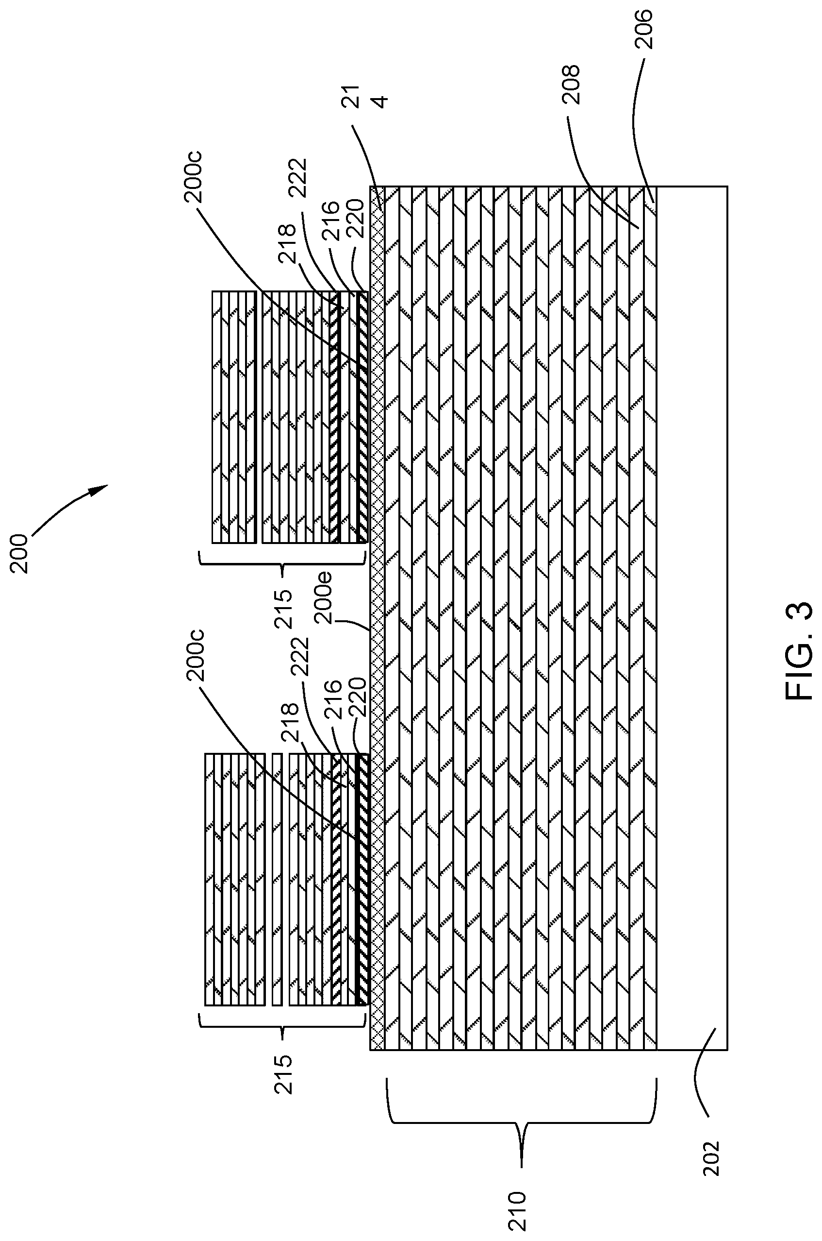
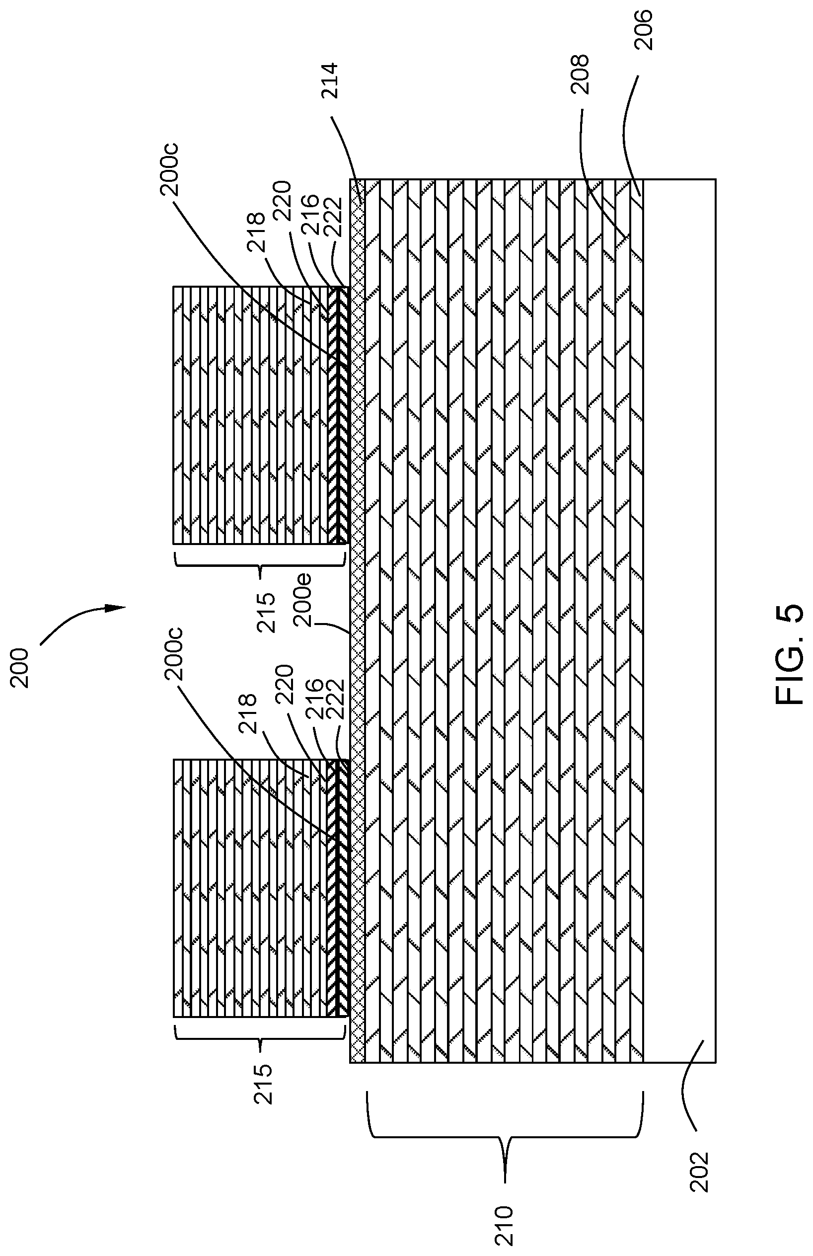
[0031] The EUV mask blank 200, which may be a phase shift mask comprises a substrate 202, a multilayer stack of reflective layers 210 on the substrate, the multilayer stack of reflective layers 210 including a plurality of reflective layer pairs configured to reflect incident light having an intensity I.sub.0 and a phase .PHI..sub.0. The incident light is reflected from exposed area 200e which is not covered by a multilayer absorber 215. The EUV mask blank further comprises a capping layer 214 on the multilayer stack of reflective layers 210. The multilayer stack 210 of reflecting layers comprises a first reflective layer 206, second reflective layer 208.
[0032] The mask blank 200 further comprises a multilayer stack of absorber layers 215 on the capping layer 214, the multilayer stack of absorber layers 215 including a plurality of absorber layer pairs, each pair comprising a first material A and a second material B, the multilayer stack of absorber layers 215 configured to reflect incident light having an I.sub.1 and a phase .PHI..sub.1. As shown in FIG.1 the multilayer stack of absorber layers 215 provides a covered area 200c on the capping layer on the multilayer stack of reflective layers 210.
[0033] As shown in FIGS. 2-5, the EUV mask blank 200 further comprises a spacing layer 220 disposed between the capping layer 214 and the multilayer stack of absorber layers 215 and a phase tuning layer 222 in contact with one of the first material A and the second material B.
[0034] In a second embodiment, the extreme ultraviolet (EUV) mask blank 200 comprises a spacing layer 220 which as thickness configured to tune intensity of incident light reflected from the multilayer stack of absorber layers (I.sub.1) at a specific wavelength, for example, 13.53 nm.
[0035] In a third embodiment, the first or second embodiment can include the feature of the multilayer stack of absorber layers 215 covering a portion of the capping layer 214 such that there is a covered area 200c covered by the multilayer absorber area 215 and an exposed area 2003 not covered by multilayer stack of absorber layers 215, and the phase tuning layer 222 has thickness configured to tune the phase of light reflected from the multilayer stack of reflective layers so that there is a change in phase .DELTA..PHI.=.PHI..sub.1-.PHI..sub.0 that is in a range of from 120.degree. to 240.degree.. In specific embodiments, the change in phase is 180.degree..
[0036] In a fourth embodiment, as shown in FIG. 2, the first through third embodiments can include the feature that the phase tuning layer 222 is on top of the multilayer stack of absorber layers 215 and the spacing layer 220 is directly on the capping layer 214. In a fifth embodiment, as shown in FIG. 3, the first through third embodiments can include the feature that the phase tuning layer 22 is located within the multilayer stack of absorber layers 215 and the spacing layer 220 is directly on the capping layer 214. In a sixth embodiment, as shown in FIG. 4, the first through third embodiments can include the feature that the phase tuning layer 222 is directly on the spacing layer 220, and the spacing layer 220 is directly on the capping layer 214. In a seventh embodiment, as shown in FIG. 5, the first through third embodiments can include the feature that the spacing layer 220 is directly on the phase tuning layer 222, and the phase tuning layer 222 is directly on the capping layer 214.
[0037] In an eighth embodiment, the extreme ultraviolet (EUV) mask blank 200 of the first seven embodiments can be modified so that the reflective layer pairs comprise molybdenum (Mo) and silicon (Si) and the first material A comprises molybdenum (Mo) and the second material B comprises silicon (Si).
[0038] In a ninth embodiment, the first through eighth embodiments can be modified so that the spacing layer 200 comprises a material having an extinction coefficient K less than 0.04. For example, the spacing layer 220 can comprise a material comprising an element selected from the group consisting of Ru, W, Mn, Mo, Nb, Hf, Ti, Zr, Mg, Al Ge, Se, and Si. In one or more embodiments, the spacing layer 220 can comprise oxides, nitrides, carbides, borides and alloys of these elements.
[0039] In a tenth embodiment, the extreme ultraviolet (EUV) mask blank of the first through ninth embodiments can be modified so that the phase tuning layer 222 comprises a material having a refraction coefficient n greater than 0.92. In one or more embodiments, the tuning layer 222 comprises a material comprising an element selected from the group consisting of Cr, Ta, Ti, Fe, Co, Ni, Cu, Zn, Te, Bi, Cd, Ga. In one or more embodiments, the phase tuning layer 222 can comprise oxides, nitrides, carbides, borides and alloys of these elements.
[0040] In specific embodiments, the spacing layer 220 thickness is in a range of 20-50 nm, for example 30-45 nm or 32-40 nm. Intensity I1 at 13.53 nm as a function of spacing layer thickness for a silicon spacing layer varying from 32 to 40 nm is shown in FIG. 7A for an EUV reflective element include a chromium 10 Angstrom thick phase change layer with 14 Mo/Si absorber layer pairs. FIG. 7B shows a phase change .DELTA..PHI.=.PHI..sub.1-.PHI..sub.0 at 13.53 nm as a function of phase tuning layer thickness for a the chromium 10 Angstrom thick phase change layer with 14 Mo/Si absorber layer pairs.
[0041] Another aspect of the disclosure pertains to a method of manufacturing an extreme ultraviolet (EUV) mask blank. In an eleventh embodiment, the method comprises depositing a multilayer stack of reflective layers on a substrate, the multilayer stack of reflective layers including a plurality of reflective layer pairs configured to reflect incident light having an intensity I.sub.0 and a phase .PHI..sub.0 and then depositing a capping layer on the multilayer stack of reflecting layers. The method further comprises depositing a multilayer stack of absorber layers on the capping layer, the multilayer stack of absorber layers including a plurality of absorber layer pairs, each pair comprising a first material A and a second material B, the multilayer stack of absorber layers configured to reflect incident light having an I.sub.1 and a phase .PHI..sub.1. The method also comprises forming a spacing layer between the capping layer and the multilayer stack of absorber layers and a phase tuning layer in contact with one of the first material A and the second material B.
[0042] In a twelfth embodiment, the spacing layer has thickness configured to tune intensity of incident light reflected from the multilayer stack of absorber layers (I.sub.1) at a specific wavelength. In a thirteenth embodiment, the multilayer stack of absorber layers covers a portion of the capping layer such that there is a covered area by the multilayer absorber area and an exposed area not covered by multilayer stack of absorber layers, and wherein the phase tuning layer has thickness configured to tune the phase of light reflected from the multilayer stack of reflective layers so that there is a change in phase .DELTA..PHI.=.PHI..sub.1-I.sub.0 that is in a range of from 120.degree. to 240.degree.. In a fourteenth embodiment, the phase tuning layer is deposited on top of the multilayer stack of absorber layers and the spacing layer is deposited directly on the capping layer.
[0043] In a fifteenth embodiment, the phase tuning layer is located within the multilayer stack of absorber layers and the spacing layer is deposited directly on the capping layer. In a sixteenth embodiment, the phase tuning layer is deposited directly on the spacing layer, and the spacing layer is deposited directly on the capping layer. In a seventeenth embodiment, the spacing layer is deposited directly on the phase tuning layer, and the phase tuning layer is deposited directly on the capping layer.
[0044] In an eighteenth embodiment, the reflective layer pairs comprise molybdenum (Mo) and silicon (Si) and the first material A comprises molybdenum (Mo) and the second material B comprises silicon (Si). In a nineteenth embodiment, the spacing layer comprises a material having an extinction coefficient K less than 0.04. In another embodiment of the method, the spacing layer comprises a material comprising an element selected from the group consisting of Ru, W, Mn, Mo, Nb, Hf, Ti, Zr, Mg, Al Ge, Se, and Si. Some embodiments include oxides, nitrides, carbides, borides and alloys of these elements. In another embodiment of the method, the phase tuning layer comprises a material having a refraction coefficient n greater than 0.92. For example, the phase tuning layer can comprise a material comprising an element selected from the group consisting of Cr, Ta, Ti, Fe, Co, Ni, Cu, Zn, Te, Bi, Cd, Ga. Some embodiments include oxides, nitrides, carbides, borides and alloys of these elements.
[0045] A twentieth embodiment includes an extreme ultraviolet reflective element lithography system comprises an extreme ultraviolet light source which produces extreme ultraviolet light; a reflective element configured to reflect the extreme ultraviolet light, the reflective element including: a substrate; a multilayer stack of reflective layers on the substrate, the multilayer stack of reflective layers including a plurality of reflective layer pairs configured to reflect incident light having an intensity I.sub.0 and a phase .PHI..sub.0; a capping layer on the multilayer stack of reflecting layers; a multilayer stack of absorber layers on the capping layer, the multilayer stack of absorber layers including a plurality of absorber layer pairs, each pair comprising a first material A and a second material B, the multilayer stack of absorber layers configured to reflect incident light having an I.sub.1 and a phase .PHI..sub.1; and a spacing layer disposed between the capping layer and the multilayer stack of absorber layers and a phase tuning layer in contact with one of the first material A and the second material B. In one or more embodiments, the extreme ultraviolet reflective element lithography system comprises any of the first through tenth embodiments described above with respect to the EUV mask blank and FIGS. 2-5,
[0046] In one or more embodiments, the substrate 202 is an element for providing structural support to the extreme ultraviolet reflective element 200. In one or more embodiments, the substrate 202 is made from a material having a low coefficient of thermal expansion (CTE) to provide stability during temperature changes. In one or more embodiments, the substrate 202 has properties such as stability against mechanical cycling, thermal cycling, crystal formation, or a combination thereof. The substrate 202 according to one or more embodiments is formed from a material such as silicon, glass, oxides, ceramics, glass ceramics, or a combination thereof.
[0047] According to one or more embodiments, the multilayer stack of reflective layers 210 include the first reflective layer 206 and the second reflective layer 208, which form a reflective pair. In a non-limiting embodiment, the multilayer stack of reflective layers 210 includes a range of about 20 to about 60 of the reflective pairs for a total of up to 120 reflective layers.
[0048] The first reflective layer 206 and the second reflective layer 208 can be formed from a variety of materials. In one or more embodiments, the first reflective layer 206 and the second reflective layer 208 are formed from silicon and molybdenum, respectively. Although the layers are shown as silicon and molybdenum, it is understood that the alternating layers can be formed from other materials or have other internal structures.
[0049] The first reflective layer 206 and the second reflective layer 208 can have a variety of structures. In one or more embodiments, both the first reflective layer 206 and the second reflective layer 208 are formed with a single layer, multiple layers, a divided layer structure, non-uniform structures, or a combination thereof.
[0050] Because most materials absorb light at extreme ultraviolet wavelengths, the optical elements used are reflective instead of the transmissive as used in other lithography systems. The multilayer stack of reflective layers 210 forms a reflective structure by having alternating thin layers of materials with different optical properties to create a Bragg reflector or mirror.
[0051] In one or more embodiments, each of the alternating layers 206, 208 has dissimilar optical constants for the extreme ultraviolet light. The alternating layers 206, 208 provide a resonant reflectivity when the period of the thickness of the alternating layers 206, 208 is one half the wavelength of the extreme ultraviolet light. In one or more embodiments, for the extreme ultraviolet light at a wavelength of 13 nm, the alternating layers 206, 208 are about 6.5 nm thick.
[0052] The multilayer stack of reflective layers 210 can be formed in a variety of ways. In an embodiment, the first reflective layer 206 and the second reflective layer 208 are formed by magnetron sputtering, ion sputtering systems, pulsed laser deposition, cathode arc deposition, or a combination thereof.
[0053] In an illustrative embodiment, the multilayer stack of reflective layers 210 is formed using a physical vapor deposition technique, such as magnetron sputtering. In an embodiment, the first reflective layer 206 and the second reflective layer 208 of the multilayer stack 210 have the characteristics of being formed by the magnetron sputtering technique including precise thickness, low roughness, and clean interfaces between the layers. In an embodiment, the first reflective layer 206 and the second reflective layer 208 the multilayer stack of reflective layers 210 have the characteristics of being formed by the physical vapor deposition including precise thickness, low roughness, and clean interfaces between the layers.
[0054] The physical dimensions of the layers of the multilayer stack of reflective layers 210 formed using the physical vapor deposition technique can be precisely controlled to increase reflectivity. In an embodiment, the first reflective layer 206, such as a layer of silicon, has a thickness of 4.1 nm. The second reflective layer 208, such as a layer of molybdenum, has a thickness of 2.8 nm. The thickness of the layers dictates the peak reflectivity wavelength of the extreme ultraviolet reflective element. If the thickness of the layers is incorrect, the reflectivity at the desired wavelength 13.53 nm can be reduced.
[0055] In an embodiment, the multilayer stack of reflective layers 210 has a reflectivity of greater than 60%. In an embodiment, the multilayer stack 210 formed using physical vapor deposition has a reflectivity in a range of 66%-67%. In one or more embodiments, forming the capping layer 214 over the multilayer stack of reflective layers 210 formed with harder materials improves reflectivity. In some embodiments, reflectivity greater than 70% is achieved using low roughness layers, clean interfaces between layers, improved layer materials, or a combination thereof.
[0056] In one or more embodiments, the capping layer 214 is a protective layer allowing the transmission of the extreme ultraviolet light. In an embodiment, the capping layer 214 is formed directly on the multilayer stack of reflective layers 210. In one or more embodiments, the capping layer 214 protects the multilayer stack 210 from contaminants and mechanical damage. In one embodiment, the multilayer stack of reflective layers 210 is sensitive to contamination by oxygen, carbon, hydrocarbons, or a combination thereof. The capping layer 214 according to an embodiment interacts with the contaminants to neutralize them.
[0057] In one or more embodiments, the capping layer 214 is an optically uniform structure that is transparent to the extreme ultraviolet light. The extreme ultraviolet light passes through the capping layer 214 to reflect off of the multilayer stack of reflective layers 210. In one or more embodiments, the capping layer 214 has a total reflectivity loss of 1% to 2%. In one or more embodiments, each of the different materials has a different reflectivity loss depending on thickness, but all of them will be in a range of 1% to 2%.
[0058] In one or more embodiments, the capping layer 214 has a smooth surface. For example, the surface of the capping layer 214 can have a roughness of less than 0.2 nm RMS (root mean square measure). In another example, the surface of the capping layer 214 has a roughness of 0.08 nm RMS for a length in a range of 1/100 nm and 1/1 .mu.m. The RMS roughness will vary depending on the range it is measured over. For the specific range of 100 nm to 1 micron that roughness is 0.08 nm or less. Over a larger range the roughness will be higher.
[0059] The capping layer 214 can be formed in a variety of methods. In an embodiment, the capping layer 214 is formed on or directly on the multilayer stack 210 with magnetron sputtering, ion sputtering systems, ion beam deposition, electron beam evaporation, radio frequency (RF) sputtering, atomic layer deposition (ALD), pulsed laser deposition, cathode arc deposition, or a combination thereof. In one or more embodiments, the capping layer 214 has the physical characteristics of being formed by the magnetron sputtering technique including precise thickness, low roughness, and clean interfaces between the layers. In an embodiment, the capping layer 214 has the physical characteristics of being formed by the physical vapor deposition including precise thickness, low roughness, and clean interfaces between the layers.
[0060] In one or more embodiments, the capping layer 214 is formed from a variety of materials having a hardness sufficient to resist erosion during cleaning. In one embodiment, ruthenium is used as a capping layer material because it is a good etch stop and is relatively inert under the operating conditions. However, it is understood that other materials can be used to form the capping layer 214. In specific embodiments, the capping layer 214 has a thickness of in a range of 2.5 and 5.0 nm.
[0061] In one or more embodiments, multilayer absorber 215 is a plurality of layers that absorbs the extreme ultraviolet light.
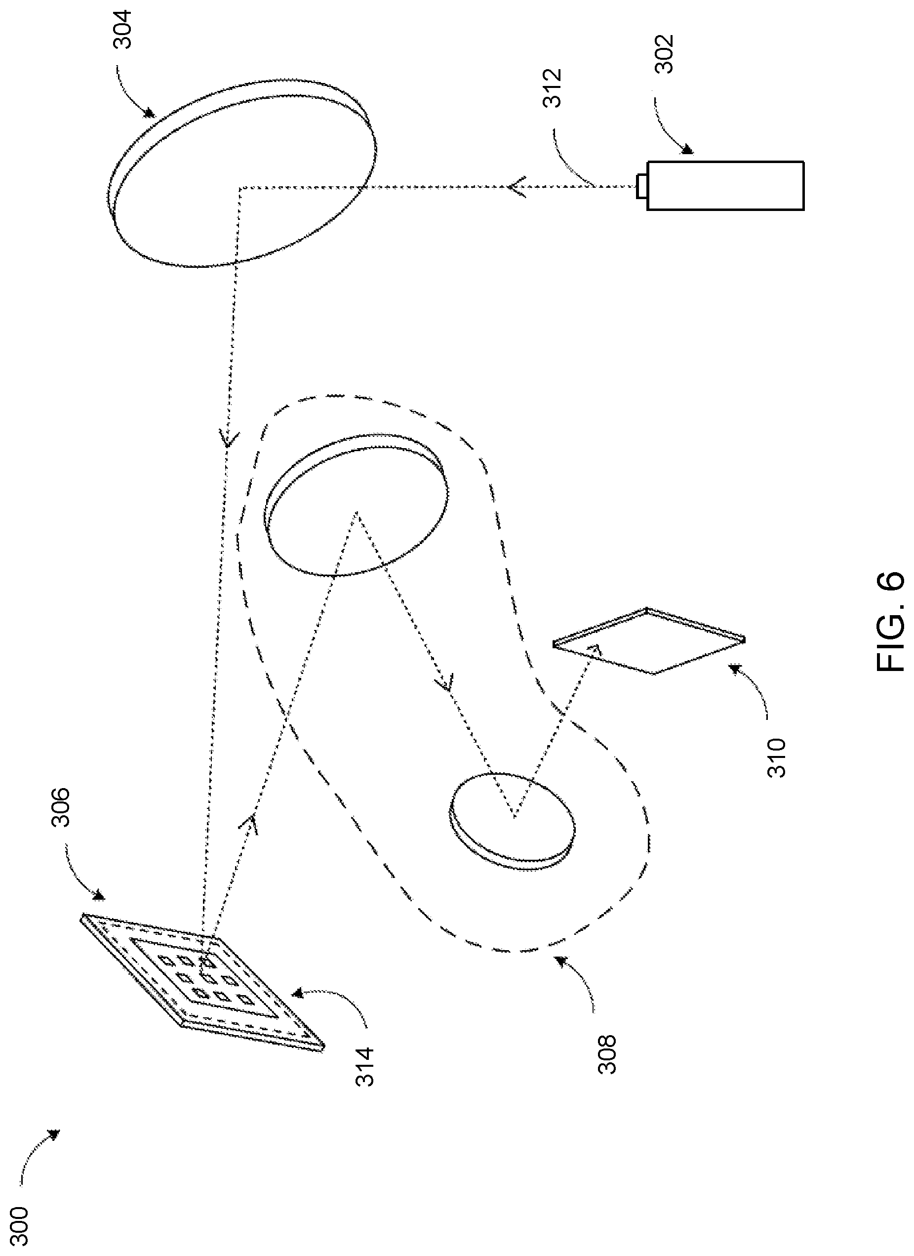
[0062] Referring now to FIG. 6, an exemplary embodiment of an extreme ultraviolet lithography system 300 is shown. The extreme ultraviolet lithography system 300 includes an extreme ultraviolet light source 302 which produces extreme ultraviolet light 312, a set of reflective elements, and a target substrate or wafer 310. The reflective elements include a condenser 304, an EUV reflective mask 306, an optical reduction assembly 308, a mask blank, a mirror, or a combination thereof.
[0063] The extreme ultraviolet light source 302 generates the extreme ultraviolet light 312. The extreme ultraviolet light 312 is electromagnetic radiation having a wavelength in a range of 5 to 50 nanometers (nm). For example, the extreme ultraviolet light source 302 includes a laser, a laser produced plasma, a discharge produced plasma, a free-electron laser, synchrotron radiation, or a combination thereof.
[0064] In one or more embodiments, the extreme ultraviolet light source 302 produces the extreme ultraviolet light 312 having a narrow bandwidth. For example, the extreme ultraviolet light source 302 generates the extreme ultraviolet light 312 at 13.53 nm. The center of the wavelength peak is 13.53 nm.
[0065] The condenser 304 is an optical unit for reflecting and focusing the extreme ultraviolet light 312. The condenser 304 reflects and concentrates the extreme ultraviolet light 312 from the extreme ultraviolet light source 302 to illuminate the EUV reflective mask 306.
[0066] Although the condenser 304 is shown as a single element, it is understood that the condenser 304 can include one or more reflective elements such as concave mirrors, convex mirrors, flat mirrors, or a combination thereof, for reflecting and concentrating the extreme ultraviolet light 312. For example, the condenser 304 can be a single concave mirror or an optical assembly having convex, concave, and flat optical elements.
[0067] The EUV reflective mask 306 is an extreme ultraviolet reflective element having a mask pattern 314. The EUV reflective mask 306 creates a lithographic pattern to form a circuitry layout to be formed on the target wafer 310. The EUV reflective mask 306 reflects the extreme ultraviolet light 312. The mask pattern 314 defines a portion of a circuitry layout.
[0068] The optical reduction assembly 308 is an optical unit for reducing the image of the mask pattern 314. The reflection of the extreme ultraviolet light 312 from the EUV reflective mask 306 is reduced by the optical reduction assembly 308 and reflected on to the target wafer 310. The optical reduction assembly 308 can include mirrors and other optical elements to reduce the size of the image of the mask pattern 314. For example, the optical reduction assembly 308 can include concave mirrors for reflecting and focusing the extreme ultraviolet light 312.
[0069] The optical reduction assembly 308 reduces the size of the image of the mask pattern 314 on the target wafer 310. For example, the mask pattern 314 can be imaged at a 4:1 ratio by the optical reduction assembly 308 on the target wafer 310 to form the circuitry represented by the mask pattern 314 on the target wafer 310. The extreme ultraviolet light 312 can scan the reflective mask 306 synchronously with the target substrate or wafer 310 to form the mask pattern 314 on the target substrate or wafer 310.
[0070] Thus, any of the extreme ultraviolet elements described with respect to the first through tenth embodiments and FIGS. 2-5 herein are be used to provide extreme ultraviolet mirror or an EUV mask blank. An EUV mirror is a multilayered structure reflective in a range of extreme ultraviolet light. The extreme ultraviolet mirror can be formed using semiconductor fabrication techniques. An EUV mask blank and an extreme ultraviolet mirror can be similar structures with respect to the layers formed on each element, however, the extreme ultraviolet mirror does not have a mask pattern.
[0071] In specific embodiments, the spacing layer 220 thickness is in a range of 20-50 nm, for example 30-45 nm or 32-40 nm. Intensity I1 at 13.53 nm as a function of spacing layer thickness for a silicon spacing layer varying from 32 to 40 nm is shown in FIG. 7A for an EUV reflective element include a chromium 10 Angstrom thick phase change layer with 14 Mo/Si absorber layer pairs. FIG. 7B shows a phase change .DELTA..PHI.=.PHI..sub.1-.PHI..sub.0 at 13.53 nm as a function of phase tuning layer thickness for a the chromium 10 Angstrom thick phase change layer with 14 Mo/Si absorber layer pairs.
[0072] Reference throughout this specification to "one embodiment," "certain embodiments," "one or more embodiments" or "an embodiment" means that a particular feature, structure, material, or characteristic described in connection with the embodiment is included in at least one embodiment of the disclosure. Thus, the appearances of the phrases such as "in one or more embodiments," "in certain embodiments," "in one embodiment" or "in an embodiment" in various places throughout this specification are not necessarily referring to the same embodiment of the disclosure. Furthermore, particular features, structures, materials, or characteristics may be combined in any suitable manner in one or more embodiments.
[0073] Although the disclosure herein has been described with reference to particular embodiments, it is to be understood that these embodiments are merely illustrative of the principles and applications of the present disclosure. It will be apparent to those skilled in the art that various modifications and variations can be made to the method and apparatus of the present disclosure without departing from the spirit and scope of the disclosure. Thus, it is intended that the present disclosure include modifications and variations that are within the scope of the appended claims and their equivalents.
* * * * *
D00000
D00001
D00002
D00003
D00004
D00005
D00006
D00007
XML
uspto.report is an independent third-party trademark research tool that is not affiliated, endorsed, or sponsored by the United States Patent and Trademark Office (USPTO) or any other governmental organization. The information provided by uspto.report is based on publicly available data at the time of writing and is intended for informational purposes only.
While we strive to provide accurate and up-to-date information, we do not guarantee the accuracy, completeness, reliability, or suitability of the information displayed on this site. The use of this site is at your own risk. Any reliance you place on such information is therefore strictly at your own risk.
All official trademark data, including owner information, should be verified by visiting the official USPTO website at www.uspto.gov. This site is not intended to replace professional legal advice and should not be used as a substitute for consulting with a legal professional who is knowledgeable about trademark law.