Photoresist Compositions And Methods For Fabricating Semiconductor Devices Using The Same
KOH; CHAWON ; et al.
U.S. patent application number 16/399473 was filed with the patent office on 2020-11-05 for photoresist compositions and methods for fabricating semiconductor devices using the same. The applicant listed for this patent is Inpria Corporation, Samsung Electronics Co., Ltd.. Invention is credited to Brian Cardineau, SOO YOUNG CHOI, CHAWON KOH, TSUNEHIRO NISHI, Jason Stowers, Sangyoon Woo.
| Application Number | 20200348594 16/399473 |
| Document ID | / |
| Family ID | 1000004069628 |
| Filed Date | 2020-11-05 |


| United States Patent Application | 20200348594 |
| Kind Code | A1 |
| KOH; CHAWON ; et al. | November 5, 2020 |
PHOTORESIST COMPOSITIONS AND METHODS FOR FABRICATING SEMICONDUCTOR DEVICES USING THE SAME
Abstract
Provided herein are photoresist compositions and methods for fabricating semiconductor devices using the same. A photoresist composition may include an organometallic material, a fluorine-containing material, and an organic solvent.
| Inventors: | KOH; CHAWON; (Yongin-si, KR) ; NISHI; TSUNEHIRO; (Seongnam-si, KR) ; Cardineau; Brian; (Corvallis, OR) ; Woo; Sangyoon; (Leuven, BE) ; Stowers; Jason; (Corvallis, OR) ; CHOI; SOO YOUNG; (Hwaseong-si, KR) | ||||||||||
| Applicant: |
|
||||||||||
|---|---|---|---|---|---|---|---|---|---|---|---|
| Family ID: | 1000004069628 | ||||||||||
| Appl. No.: | 16/399473 | ||||||||||
| Filed: | April 30, 2019 |
| Current U.S. Class: | 1/1 |
| Current CPC Class: | G03F 7/11 20130101; H01L 21/31144 20130101; G03F 7/0042 20130101; G03F 7/2004 20130101; G03F 7/325 20130101; H01L 21/0274 20130101 |
| International Class: | G03F 7/11 20060101 G03F007/11; G03F 7/004 20060101 G03F007/004; G03F 7/20 20060101 G03F007/20; H01L 21/027 20060101 H01L021/027; H01L 21/311 20060101 H01L021/311 |
Claims
1. A photoresist composition, comprising: an organometallic material; a fluorine-containing material; and an organic solvent.
2. The photoresist composition of claim 1, wherein the organometallic material is an organometallic nano-cluster material, and wherein the fluorine-containing material is a fluorine-containing polymer material.
3. The photoresist composition of claim 1, wherein the organometallic material is present in the photoresist composition in an amount of 0.1-99 wt. % of the photoresist composition, the fluorine-containing material is present in the photoresist composition in an amount of 0.1-30 wt. % of the photoresist composition, and the organic solvent is present in the photoresist composition in an amount of 0.9-99.8 wt. % of the photoresist composition.
4. The photoresist composition of claim 1, wherein the organometallic material comprises at least one metal selected from the group consisting of: tin (Sn), indium (In), antimony(Sb), and hafnium (Hf).
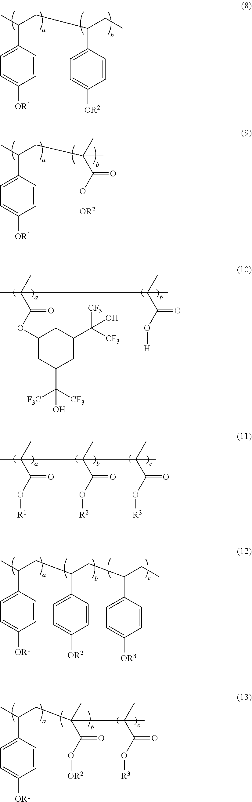
5. The photoresist composition of claim 1, wherein: the fluorine-containing material has a structure represented by one of formula (1) to (14): ##STR00004## ##STR00005## ##STR00006## wherein: a, b and c, if present, are each independently a natural number; R.sup.1, if present, is fluorine; R.sup.2, if present, is each independently hydrogen or a hydrophilic group; and R.sup.3, if present, is a hydrophobic group; and wherein, in formulae (7) to (10), a/(a+b) is 0.1-1 and b/(a+b) is 0.0-0.9; and wherein, in formulae (11) to (14), a/(a+b+c) is 0.0-0.9, b/(a+b+c) is 0.1-1, and c/(a+b+c) is 0.0-0.9.
6. The photoresist composition of claim 1, wherein the fluorine-containing material comprises at least one functional group selected from the group consisting of --CFOH, --CHCFOH, --CHCFCFOH, --C(CF)OH, --CFCF(CF)OH, and --CHC(CF)OH.
7. The photoresist composition of claim 1, wherein the organic solvent comprises methyl isobutyl carbinol (MIBC), ether, propylene glycol monomethylether acetate (PGMEA), propylene glycol monomethylether (PGME), ethyl lactate (EL), and/or .beta.-hydroxy .beta.-methylbutyric acid (HBM).
8. The photoresist composition of claim 1, further comprising a surfactant in an amount of 0.01-3 wt. % of the photoresist composition.
9. The photoresist composition of claim 1, wherein the organometallic material has a chemical formula represented by one of formula (15) to (17):, R.sub.wMeO.sub.(2-(w-2)-(x/2))(OH).sub.x (15) R.sub.yMeL.sub.4-y (16) RMeO.sub.(3/2-z/2)(OH).sub.z (17) wherein: R is a hydrocarbon compound having 1 to 30 carbon atoms and includes at least one atom selected from carbon, nitrogen and oxygen, Me is selected from the group consisting of: tin (Sn), indium (In), antimony (Sb), and hafnium (Hf); and wherein, in formula (15), 0<w.ltoreq.2 and 0<(w+x).ltoreq.4, in formula (16), y is 1 or 2, and L is a metal ligand, and, in formula (17), 0<z<3.
10. The photoresist composition of claim 1, further comprising a moisture absorbent in an amount of 0.01-10 wt. % of the photoresist composition.
11. The photoresist composition of claim 10, wherein the moisture absorbent is selected from the group consisting of polyoxyethylene nonylphenolether, R.sup.5C.sub.6H.sub.4C(CH.sub.2CH.sub.2O).sub.nH, polyethylene glycol (PEG), HO(CH.sub.2CH.sub.2O).sub.nH, and polyacrylamide, wherein R.sup.5 is a hydrocarbon compound having 1 to 30 carbon atoms and includes at least one atom selected from carbon, nitrogen and oxygen and n is a natural number selected from 1 to 1,000.
12. The photoresist composition of claim 1, further comprising water in an amount of 0.001-0.1 wt. % of the photoresist composition.
13. A method for fabricating a semiconductor device, the method comprising: providing a photoresist composition including an organometallic material, a fluorine-containing material, and an organic solvent; forming a photoresist film by coating a substrate with the photoresist composition, wherein the photoresist film includes a photosensitive film and a moisture barrier layer on the photosensitive film, wherein the photosensitive film comprises the organometallic material and the moisture barrier layer comprises the fluorine-containing material; evaporating the organic solvent using a soft bake process; converting a portion of the photosensitive film into a mask pattern using an exposure process and a post bake process; and removing the photosensitive film and leaving the mask pattern using a development process.
14. The method of claim 13, further comprising removing the moisture barrier layer using the development process.
15. The method of claim 13, wherein the development process is performed using n-butyl acetate or 2-heptanone.
16. The method of claim 13, wherein the photosensitive film has a thickness of 1 nm-30 nm, and the moisture barrier layer has a thickness of 0.5 nm-25 nm.
17. A method for fabricating a semiconductor device, the method comprising: forming a photosensitive film and a moisture barrier layer on a substrate, wherein the photosensitive film and the moisture barrier layer are sequentially stacked on the substrate; converting a portion of the photosensitive film into a mask pattern using an exposure process and a post bake process; and removing the photosensitive film and leaving the mask pattern using a development process.
18. The method of claim 17, wherein forming the photosensitive film and the moisture barrier layer on the substrate comprises: providing a photoresist composition including an organometallic material, a fluorine-containing material, and an organic solvent; and forming a photoresist film by coating the substrate with the photoresist composition, wherein the photoresist film includes the photosensitive film and the moisture barrier layer, and wherein the photosensitive film comprises the organometallic material and the moisture barrier layer comprises the fluorine-containing material.
19. The method of claim 18, further comprising, prior to the exposure process, evaporating the organic solvent from the photoresist film using a soft bake process.
20. The method of claim 17, wherein the moisture barrier layer is removed using the development process.
Description
FIELD
[0001] The disclosure herein relates to photoresist compositions and methods for fabricating semiconductor devices using the same.
BACKGROUND
[0002] Semiconductor devices have been highly integrated. Thus, finer and more precise patterning is needed in preparing semiconductor devices. Accordingly, an exposure process using extreme ultraviolet (EUV) having a wavelength of 13.4 nm as a light source has been utilized. The EUV is absorbed entirely in a conventional photoresist film due to a very short wavelength thereof, which makes forming a precise pattern difficult. Therefore, in a photolithography process using EUV as a light source, a new photoresist material capable of transmitting the EUV may be useful to allow for precise and fine patterning.
SUMMARY
[0003] The present disclosure provides a photoresist composition capable of providing a precise pattern.
[0004] The present disclosure also provides a method for fabricating a semiconductor device that is capable of forming a precise pattern.
[0005] An embodiment of the inventive concepts provides a photoresist composition including: an organometallic material; a fluorine-containing material; and an organic solvent.
[0006] In an embodiment of the inventive concepts, a method for fabricating a semiconductor device includes: providing a photoresist composition including an organometallic material, a fluorine-containing material, and an organic solvent; forming a photoresist film by coating a substrate with the photoresist composition, wherein the photoresist film includes a photosensitive film and a moisture barrier layer positioned on the photosensitive film, wherein the photosensitive film comprises the organometallic material and the moisture barrier layer comprises the fluorine-containing material; evaporating the organic solvent through a soft bake process; converting a portion of the photosensitive film into a mask pattern through an exposure process and a post bake process; and removing the photosensitive film and leaving the mask pattern through a development process.
[0007] In an embodiment, a method for fabricating a semiconductor device includes: forming a photosensitive film and a moisture barrier layer sequentially stacked on a substrate; converting a portion of the photosensitive film into a mask pattern through an exposure process and a post bake process; and removing the photosensitive film and leaving the mask pattern through a development process.
BRIEF DESCRIPTION OF THE FIGURES
[0008] The accompanying drawings are included to provide a further understanding of the inventive concepts, and are incorporated in and constitute a part of this specification. The drawings illustrate exemplary embodiments of the inventive concepts and, together with the description, serve to explain principles of the inventive concepts.
[0009] FIG. 1 is a flowchart showing a method for fabricating a semiconductor device according to an example embodiment of the inventive concepts.
[0010] FIGS. 2A to 2F are cross-sectional views sequentially illustrating processes of a method for fabricating a semiconductor device according to an example embodiment of the inventive concepts.
DETAILED DESCRIPTION
[0011] Hereinafter, exemplary embodiments of the inventive concepts will be described in detail with reference to the accompanying drawings.
[0012] As used herein, "and/or" refers to and encompasses any and all possible combinations of one or more of the associated listed items, as well as the lack of combinations when interpreted in the alternative ("or").
[0013] FIG. 1 is a flowchart showing a method for fabricating a semiconductor device according to an example embodiment of the inventive concepts. FIGS. 2A to 2F are cross-sectional views sequentially illustrating processes of a method for fabricating a semiconductor device according to an example embodiment of the inventive concepts.
[0014] Referring to FIGS. 1 and 2A, a substrate 1 is prepared. The substrate 1 may be, for example, a silicon single crystal wafer or a silicon on insulator (SOI) substrate. An etching target film 3 may be formed on the substrate 1. The etching target film 3 may be, for example, an insulation film; a polysilicon film such as a silicon oxide film, a silicon oxynitride film or a silicon nitride film; or a conductive film such as a metal-containing film.
[0015] Subsequently, a photoresist composition is prepared or provided (S10). The photoresist composition includes a fluorine-containing material, an organometallic material, and an organic solvent. In the photoresist composition, the organometallic material may be present in an amount of 0.1-99 wt. % of the photoresist composition. In some embodiments, the organometallic material may be present in the photoresist composition in an amount of 0.1%, 1%, 5%, 10%, 15%, 20%, 25%, 30%, 35%, 40%, 45%, or 50% to 55%, 60%, 65%, 70%, 75%, 80%, 85%, 90%, 95%, or 99% by weight of the photoresist composition. The fluorine-containing material may be present in an amount of 0.1-30 wt. % of the photoresist composition. In some embodiments, the fluorine-containing material may be present in the photoresist composition in an amount of 0.1%, 1%, 5%, 10%, or 15% to 20%, 25%, or 30% by weight of the photoresist composition. The organic solvent may be present in an amount of 0.9-99.8 wt. % of the composition. In some embodiments, the organic solvent may be present in the photoresist composition in an amount of 1%, 5%, 10%, 15%, 20%, 25%, 30%, 35%, 40%, 45%, or 50% to 55%, 60%, 65%, 70%, 75%, 80%, 85%, 90%, 95%, or 99% by weight of the photoresist composition. The photoresist composition may be used for a photolithography process using an EUV light source.
[0016] The fluorine-containing material may include at least one functional group selected from: --CFOH, --CHCFOH, --CHCFCFOH, --C(CF)OH, --CFCF(CF)OH, and/or --CHC(CF)OH.
[0017] The fluorine-containing material may be a fluorine-containing polymer material. The fluorine-containing polymer material may have a structure represented by one of formula (1) to (14) below.
##STR00001## ##STR00002## ##STR00003##
[0018] In formulae (1) to (14), a, b and c, when present, may each independently be a natural number such as, for example, a natural number from 1 to 100 or 1 to 50.
[0019] In formulae (1) to (14), R.sup.1, if present, may each be fluorine. In formulae (7) to (9) and (11) to (14), R.sup.2, if present, may each independently be a hydrogen or a hydrophilic group (e.g., a polar group). The hydrophilic group may comprise a carboxyl group, a hydroxyl group and/or an amine. The hydrophilic group may be able to absorb moisture through hydrogen bonding with water. In formulae (11) to (14), R.sup.3, if present, may each independently be a hydrophobic group or a non-polar group. The non-polar group may allow for the moisture barrier layer 5b to be dissolved well in a developer during a development process. R.sup.3 in formulae (11) to (14) may comprise at least one metal such as, e.g., tin (Sn), indium (In) and/or hafnium (Hf). When R.sup.3 includes a metal, EUV absorptivity of the photosensitive film 5a may be increased, optionally compared to absorptivity of a photosensitive film not in accordance with the present inventive concepts, thereby improving sensitivity of the photosensitive film 5a.
[0020] In formulae (7) to (10), a/(a+b) may be 0.1-1 and b/(a+b) may be 0.0-0.9. In formulae (11) to (14), a/(a+b+c) may be 0.0-0.9, b/(a+b+c) may be 0.1-1, and c/(a+b+c) may be 0.0-0.9.
[0021] In some embodiments, the fluorine-containing polymer material may include: an acrylate; a methacrylate such as, e.g., shown in formula (1); and/or a methyl methacrylate (e.g., as shown in formula (2)) as a monomer or a polymer backbone. In some embodiments, the fluorine-containing polymer material may include polyhydroxy acrylate (PHS) as a monomer as shown, e.g., in formula (3). The fluorine-containing polymer material may include a cyclic fluoroalcohol material as a monomer as shown, e.g., in formulae (4) and/or (5). In some embodiments, the fluorine-containing polymer material may include a methacrylate, to which a cyclic fluoroalcohol is bonded, as a monomer as shown, e.g., in formula (6). In some embodiments, the fluorine-containing polymer material may include combinations of two or more monomers having a structure selected from formulae (1) to (6) as shown, e.g., in formulae (7) to (12).
[0022] The organometallic material may be an organometallic nano-cluster material. The organometallic material may include at least one of tin (Sn), indium (In), antimony (Sb) and hafnium (Hf). In some embodiments, the organometallic material may have a chemical formula selected from formulae (15) to (17) below.
R.sub.wMeO.sub.(2-(w-2)-(x/2))(OH).sub.x (15)
R.sub.yMeL.sub.4-y (16)
RMeO.sub.(3/2-z/2)(OH).sub.z (17)
[0023] In formulae (15) to (17), R may be a hydrocarbon compound having 1 to 30 carbon atoms and containing at least one atom selected from carbon, nitrogen and oxygen. In formulae (15) to (17), Me may be at least one of tin (Sn), indium (In), antimony (Sb) and hafnium (Hf). In formula (15), 0<w.ltoreq.2 and 0<(w+x).ltoreq.4. In formula (16), y may be 1 or 2, and L may be a metal ligand. In formula (17), 0<z<3.
[0024] The organic solvent may be at least one of methyl isobutyl carbinol (MIBC), ether, propylene glycol monomethylether acetate (PGMEA), propylene glycol monomethylether (PGME), ethyl lactate (EL), and .beta.-hydroxy .beta.-methylbutyric acid (HBM).
[0025] The photoresist composition may further include a surfactant. When the organometallic material is present in the photoresist composition in a high amount, coating failure may occur in the coating step (S20) of FIG. 1 for the photoresist composition. In this case, a surfactant may improve coating performance of the photoresist composition. Example surfactants include, but are not limited to, commercially available surfactants such as, e.g., sulfinol series of Airproduct Co. or F-series (F-410, F-444, F-477, R-08, R-30, etc.) of DIC (Dainippon Ink and Chemicals, Incorporated). A surfactant may be present in the photoresist composition in an amount of 0-3 wt. % with respect to the total weight of the photoresist composition. In some embodiments, the surfactant may be included in an amount of 0.2-0.8 wt. % of the photoresist composition. When the amount of the surfactant is more than 3 wt. % of the photoresist composition, it may increase a possibility that the film quality of the photoresist film becomes poor.
[0026] In some embodiments, the photoresist composition may include a moisture absorbent in an amount of 0-10 wt. % of the photoresist composition. The moisture absorbent may contain an amine or a super absorbent polymer. Example moisture absorbents include, but are not limited to, polyoxyethylene nonylphenolether, R.sup.5C.sub.6H.sub.4C(CH.sub.2CH.sub.2O).sub.nH, polyethylene glycol (PEG), HO(CH.sub.2CH.sub.2O).sub.nH and/or polyacrylamide, wherein R.sup.5 may be a hydrocarbon compound having 1 to 30 carbon atoms and containing at least one atom selected from carbon, nitrogen and oxygen and n is a natural number from 1 to 1000. The moisture absorbent may capture moisture, in some embodiments an excessive amount of moisture, in the air permeated into the photoresist film (reference numeral 5 in FIGS. 2A and 2B), so that the moisture absorbent may suppress or prevent a reaction between moisture and the organometallic material in the photosensitive film (reference numeral 5a in FIG. 2B).
[0027] According to some embodiments, preparing a photoresist composition may include mixing a fluorine-containing material, an organometallic material and an organic solvent. Preparing the photoresist composition may further include adding a surfactant, water and/or a moisture absorbent. In some embodiments, at least one of a surfactant, water and moisture absorbent are added to the photoresist composition.
[0028] Referring to FIGS. 1, 2A and 2B, a photoresist film 5 including a photosensitive film 5a and a moisture barrier layer 5b may be formed by coating a substrate 1 with the photoresist composition (S20). Specifically, a photoresist film 5 may be formed by coating the etching target film 3 above the substrate 1 with the photoresist composition. The photoresist film 5 may be formed to have a thickness of 1.5 nm-55 nm. The fluorine-containing material contained in the photoresist composition has a low surface energy due to the fluorine-containing monomer and, accordingly, the fluorine-containing material may move to an upper portion in the photoresist film 5 after coating. Accordingly, the moisture barrier layer 5b comprising the fluorine-containing material may be formed. The moisture barrier layer 5b may also be referred to as a fluorine-containing self-assembled moisture barrier layer.
[0029] The organometallic material contained in the photoresist composition may be positioned under the moisture barrier layer 5b, and may constitute the photosensitive film 5a. The photosensitive film may have a thickness of 1 nm-30 nm. The moisture barrier layer 5b may have a thickness of 0.5 nm-25 nm.
[0030] Referring to FIGS. 1 and 2B, a soft bake process is performed (S30), whereby the organic solvent, which may be present in the photoresist film 5 may be evaporated. Accordingly, the photoresist film 5, which includes the photosensitive film 5a and the moisture barrier film 5b, may become close to a solid state.
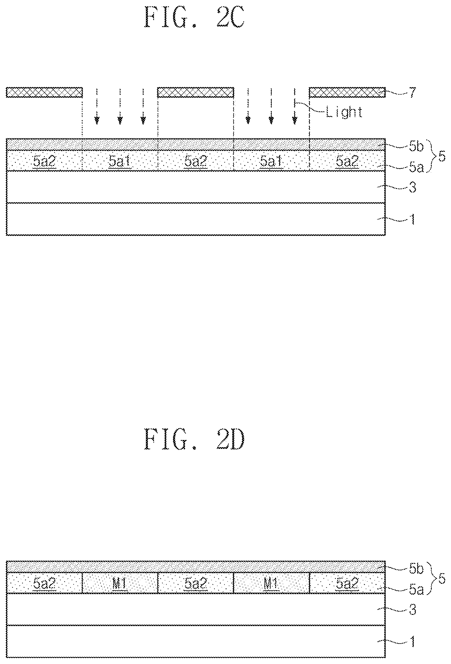
[0031] Referring to FIGS. 1 and 2C, an exposure process is performed (S40). The exposure process may be performed using an EUV light source and a photomask 7. In the exposure process, light (for example, EUV) that has been passed through the photomask 7 may be transmitted through the moisture barrier layer 5b, and may be incident into the photosensitive film 5a, whereby the photosensitive film 5a may have an exposed portion Sal and a non-exposed portion 5a2. A bond between a metal and at least one ligand of the organometallic material may be broken due to the incident light at the exposed portion Sal of the photosensitive film 5a, thereby forming a dangling bond. Accordingly, the organometallic material may comprise dangling bonds. This phenomenon does not occur in the non-exposed portion 5a2 of the photosensitive film 5a. When the fluorine-containing material constituting the moisture barrier layer 5b contains a metal (e.g., when the fluorine-containing material has a structure represented by one of formula (11) to (14) and R.sup.3 in formula (11) to (14) contains a metal), electrons may be emitted from the metal (e.g., the metal contained in R.sup.3) by the incident light in the exposure process. The emitted electrons may move to the exposed portion Sal of the photosensitive film 5a to increase EUV absorptivity, thereby improving the sensitivity of the photosensitive film 5a.
[0032] Subsequently, referring to FIGS. 1 and 2D, a post bake process may be performed (S50). In the post bake process, a hydroxyl group (--OH) present in the photoresist film 5 (e.g., from water) may be combined with the dangling bonds by heat to combine the organometallic materials, thereby providing a crosslinking reaction. Alternatively or in addition, at this time, the organometallic materials having the dangling bonds may be combined with each other, thereby providing a crosslinking reaction. Thus, the exposed portion Sal of the photosensitive film 5a may be converted into a mask pattern M1.
[0033] Referring to FIGS. 1 and 2E, a development process is performed (S60), whereby the non-exposed portion 5a2 of the photosensitive film 5a may be removed. At this time, the moisture barrier layer 5b may also be simultaneously removed. A developer used in the development process may be n-butyl acetate and/or 2-heptanone. The fluorine-containing material present in the moisture barrier layer 5b may dissolve well in the developer because of a non-polar group in the fluorine-containing material. Accordingly, only the mask pattern M1 may be left on the etching target film 3.
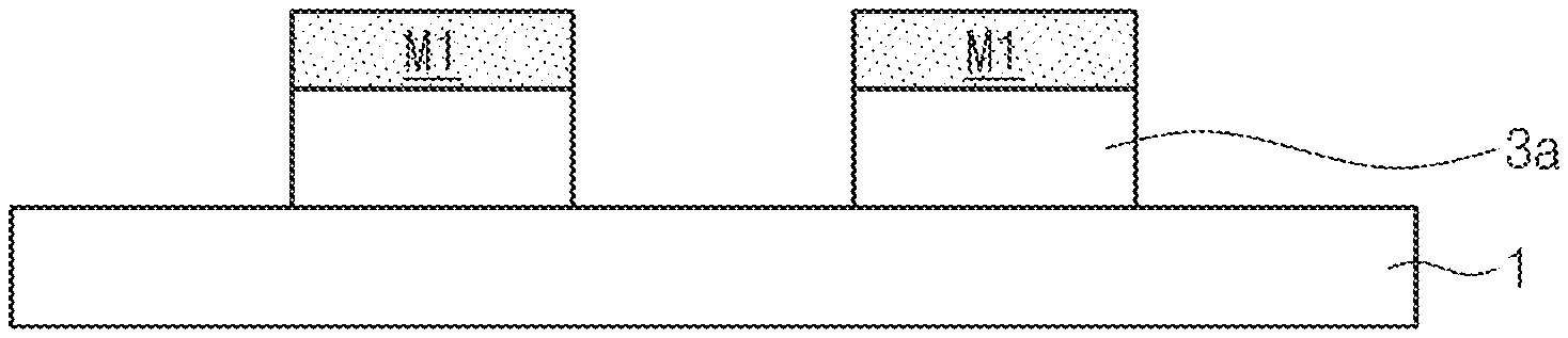
[0034] Subsequently, referring to FIG. 2F, a desired pattern 3a may be formed by etching the etching target film 3 using the mask pattern M1 as an etching mask.
[0035] The coating step (S20) with the photoresist composition, the soft bake process (S30) and the exposure process (S40) may each be performed under an atmosphere containing moisture in a predetermined amount such as, for example, atmosphere containing moisture in an amount of about 45%.
[0036] A method for fabricating a semiconductor device of the present inventive concepts uses a photoresist composition including a fluorine-containing material. Since fluorine contained in the fluorine-containing material exhibits strong hydrophobicity and/or liquid repellency, it may prevent or reduce moisture contained in the air from permeating into the photosensitive film 5a. A hydrophilic group present in the fluorine-containing material may capture moisture (e.g., an excessive amount of moisture) permeated into the photoresist film 5, which may thereby prevent or reduce the organometallic material present in the photosensitive film 5a from reacting with moisture or reduce its reaction with moisture. When the organometallic material reacts with an excessive amount of moisture, a condensation reaction may occur to form a metal oxide, which may not be dissolved in the developer and may make it difficult to form a precise pattern. However, in the present inventive concepts, it may be possible to improve this limitation by using a photoresist composition of the present inventive concepts, and a precise pattern formation may be realized.
[0037] Since the photoresist compositions of the present inventive concepts are not a chemically amplified photoresist, image degradation due to diffusion of acid, which is a limitation of a chemically amplified photoresist, does not occur and as such a precise pattern may be formed. Furthermore, the photoresist compositions of the present inventive concepts have excellent etching resistance because of an organometallic material contained in the photoresist composition, so that an etching process may be possible even with a thin thickness. Therefore, in some embodiments, since the photoresist film 5 may be formed having a thin thickness, a precise pattern may be formed by the EUV light source. The photoresist compositions according to embodiments of the present inventive concepts may increase moisture stability because of the fluorine-containing material contained in the photoresist composition.
[0038] According to some example embodiments of inventive concepts, a photoresist composition may include an organometallic material so that an etch resistance of a photoresist layer may increase. In some embodiments, the photoresist composition may include a fluorine-containing material so that moisture stability of a photoresist layer may increase. Thus, it is possible to form a precise pattern by EUV light source.
[0039] According to some example embodiments of inventive concepts, a method of fabricating a semiconductor device employs the photoresist composition. Thus, it is possible to form a precise pattern.
[0040] Although the exemplary embodiments of the present invention have been described, it is understood that the present invention should not be limited to these exemplary embodiments but various changes and modifications can be made by one ordinary skilled in the art within the spirit and scope of the present invention as hereinafter claimed.
* * * * *
D00000
D00001
D00002
D00003
D00004
XML
uspto.report is an independent third-party trademark research tool that is not affiliated, endorsed, or sponsored by the United States Patent and Trademark Office (USPTO) or any other governmental organization. The information provided by uspto.report is based on publicly available data at the time of writing and is intended for informational purposes only.
While we strive to provide accurate and up-to-date information, we do not guarantee the accuracy, completeness, reliability, or suitability of the information displayed on this site. The use of this site is at your own risk. Any reliance you place on such information is therefore strictly at your own risk.
All official trademark data, including owner information, should be verified by visiting the official USPTO website at www.uspto.gov. This site is not intended to replace professional legal advice and should not be used as a substitute for consulting with a legal professional who is knowledgeable about trademark law.