Cyclical Deposition Method Including Treatment Step And Apparatus For Same
Lee; SeungHwan ; et al.
U.S. patent application number 16/792058 was filed with the patent office on 2020-08-20 for cyclical deposition method including treatment step and apparatus for same. The applicant listed for this patent is ASM IP Holding B.V.. Invention is credited to JongHyun Ahn, KiKang Kim, SeongRyeong Kim, SungBae Kim, HakYong Kwon, SeungHwan Lee.
| Application Number | 20200266057 16/792058 |
| Document ID | 20200266057 / US20200266057 |
| Family ID | 1000004667729 |
| Filed Date | 2020-08-20 |
| Patent Application | download [pdf] |


| United States Patent Application | 20200266057 |
| Kind Code | A1 |
| Lee; SeungHwan ; et al. | August 20, 2020 |
CYCLICAL DEPOSITION METHOD INCLUDING TREATMENT STEP AND APPARATUS FOR SAME
Abstract
A method and apparatus for depositing a material on a surface of a substrate are disclosed. The method can include a treatment step to suppress a rate of material deposition on the surface of the substrate. The method can result in higher-quality deposited material. Additionally or alternatively, the method can be used to fill a recess within the surface of the substrate with reduced or no seam formation.
| Inventors: | Lee; SeungHwan; (Anseong-si, KR) ; Kwon; HakYong; (Hwaseong-si, KR) ; Kim; KiKang; (Yongin-si, KR) ; Kim; SungBae; (Cheonan-si, KR) ; Ahn; JongHyun; (Hwaseong, KR) ; Kim; SeongRyeong; (Hwaseong-si, KR) | ||||||||||
| Applicant: |
|
||||||||||
|---|---|---|---|---|---|---|---|---|---|---|---|
| Family ID: | 1000004667729 | ||||||||||
| Appl. No.: | 16/792058 | ||||||||||
| Filed: | February 14, 2020 |
Related U.S. Patent Documents
| Application Number | Filing Date | Patent Number | ||
|---|---|---|---|---|
| 62808262 | Feb 20, 2019 | |||
| Current U.S. Class: | 1/1 |
| Current CPC Class: | H01L 21/02301 20130101; H01L 21/02211 20130101; H01L 21/0217 20130101; C23C 16/45553 20130101; H01L 21/76224 20130101; C23C 16/45536 20130101; H01L 21/0228 20130101 |
| International Class: | H01L 21/02 20060101 H01L021/02; H01L 21/762 20060101 H01L021/762; C23C 16/455 20060101 C23C016/455 |
Claims
1. A method of depositing a material on a surface of a substrate surface, the method comprising the steps of: providing the substrate in a reaction chamber; forming first active species from a first reactant to modify a surface of the substrate; and performing one or more deposition cycles to deposit the material, wherein each deposition cycle comprises: introducing a second reactant to the substrate, wherein the second reactant reacts with the surface to form chemisorbed material; and forming second active species from a third reactant that react with the chemisorbed material to form deposited material, wherein a ratio of a number of steps of forming first active species and a number of deposition cycles ranges from about 1:1 to about 1:10.
2. The method of claim 1, wherein the ratio of a number of steps of forming first active species and a number of deposition cycles ranges from about 1:1 to about 1:5.
3. The method of claim 1, wherein the surface comprises silicon.
4. The method of claim 1, wherein the first active species removes one or more of hydrogen and a hydroxyl group from the surface.
5. The method of claim 1, wherein a flow of the first reactant is continuous during the step of forming first active species and the step of performing one or more deposition cycles.
6. The method of claim 5, wherein the step of forming first active species does not include a purge step.
7. The method of claim 1, further comprising a step of providing an inert gas to the reaction chamber.
8. The method of claim 7, wherein the inert gas is provided continuously during the steps of forming first active species and performing one or more deposition cycles.
9. The method of claim 1, wherein the first reactant comprises nitrogen.
10. The method of claim 9, wherein the first reactant comprises one of more of nitrogen, NH.sub.3, NO, N.sub.2O, NO.sub.2.
11. The method of claim 1, wherein the second reactant comprises silicon.
12. The method of claim 11, wherein the second reactant comprises one or more of a silane, an aminosilane, a siloxane amine, a silazane amine, an iodosilane, and a chloride.
13. The method of claim 1, wherein the third reactant comprises oxygen.
14. The method of claim 13, wherein the third reactant comprises one or more of water, hydrogen peroxide, and ozone.
15. The method of claim 1, wherein a temperature of a substrate support within the reaction chamber is less than 450.degree. C.
16. The method of claim 1, wherein a power applied to electrodes to form the second active species is about 400 W to about 1500 W.
17. The method of claim 1, wherein the steps of forming first active species and performing one or more deposition cycles are repeated until a recess on the surface is filled with the deposited material.
18. The method of claim 17, wherein the deposited material within the recess is seamless.
19. A method of depositing material on substrate surface, the method comprising the steps of: providing the substrate in a reaction chamber; forming first active species from a first reactant to modify a surface of the substrate; and performing one or more deposition cycles to deposit the material, wherein each deposition cycle comprises: introducing a second reactant to the substrate, wherein the second reactant reacts with the surface to form chemisorbed material; and forming second active species from a third reactant that react with the chemisorbed material to form deposited material, wherein a ratio of a number of steps of forming first active species and a number of deposition cycles ranges from about 1:1 to about 1:10, wherein an inert gas is continuously provided to the reaction chamber during the steps of forming first active species and performing one or more deposition cycles, and wherein a flow of the first reactant is continuous during the step of forming first active species and performing one or more deposition cycles.
20. A semiconductor processing apparatus comprising: one or more reaction chambers for accommodating a substrate comprising a surface; a first source for a first reactant in gas communication via a first valve with one of the reaction chambers; a second source for a second reactant in gas communication via a second valve with one of the reaction chambers; a third source for a third reactant in gas communication via a third valve with one of the reaction chambers; and a controller operably connected to the first, second, and third gas valves and configured and programmed to control: forming first active species from a first reactant to modify a surface of the substrate; and performing one or more deposition cycles to deposit material, wherein each deposition cycle comprises: introducing a second reactant to the substrate, wherein the second reactant reacts with the surface to form chemisorbed material; and forming second active species from a third reactant that react with the chemisorbed material to form deposited material, wherein a ratio of a number of steps of forming first active species and a number of deposition cycles ranges from about 1:1 to about 1:10.
Description
CROSS-REFERENCE TO RELATED APPLICATIONS
[0001] This application claims the benefit of U.S. Provisional Patent Application No. 62/808,262 filed on Feb. 20, 2019, the disclosure of which is incorporated herein in its entirety by reference.
FIELD OF DISCLOSURE
[0002] The present disclosure generally relates to methods and apparatus for manufacturing electronic devices. More particularly, the disclosure relates to methods and apparatus for depositing films during the formation of the electronic devices.
BACKGROUND
[0003] During manufacturing of electronic devices, such as integrated circuits, films or layers of material are often deposited onto a surface of a substrate. Such films can be patterned and etched to form desired structures. Additionally or alternatively, films can be deposited to fill recesses, such as vias, trenches, or spaces between fins, on a surface of a substrate.
[0004] In the case of filling a recess, a typical film deposition process may be subjected to drawbacks, including void formation in the recess. Voids may be formed when the deposited material forms a constriction near a top of the recess before the recess is completely filled with the deposited material. Such voids may compromise device isolation of the devices of an integrated circuit (IC) as well as the overall structural integrity of the IC. Unfortunately, preventing void formation during recess fill may place size constraints on the recesses, which may limit device packing density of the IC.
[0005] Void formation may be mitigated by decreasing recess depth and/or tapering recess sidewalls, so that the openings of the recess are wider at the top than at the bottom of the recess. A trade off in decreasing the recess depth may be reducing the effectiveness of the device isolation, while the larger top openings of recesses with tapering sidewalls may use up additional IC real estate. Such problems can become increasingly problematic when attempting to reduce device dimensions. Furthermore, it may be generally desirable to form films of relatively high quality--e.g., films having relatively high etch rates in, for example, hydrofluoric and/or phosphoric acid. Accordingly, improved methods and apparatus for forming high-quality films and/or for filling a recess are desired.
SUMMARY
[0006] Various embodiments of the present disclosure relate to methods of depositing a material onto a surface of a substrate and to apparatus for depositing the material. While the ways in which various embodiments of the present disclosure address drawbacks of prior methods are discussed in more detail below, in general, exemplary embodiments of the disclosure provide improved methods and apparatus for depositing high-quality material and/or to methods for seamlessly filling high aspect ratio recesses with the deposited material. As set forth in more detail below, exemplary methods can include a step of treating a surface of a substrate to inhibit or slow a growth rate of the deposited material. The growth-rate inhibition is thought to improve a quality of the deposited material and/or to facilitate seamless filling of a recess with the deposited material. Additionally, high-quality material can be deposited, without post-treatment annealing of the deposited material that is otherwise often performed to improve the quality of the deposited material.
[0007] In accordance with at least one embodiment of the disclosure, a method of depositing a material on a surface of a substrate surface includes the steps of: providing the substrate in a reaction chamber; forming first active species from a first reactant to modify a surface of the substrate; and performing one or more deposition cycles to deposit the material. Each deposition cycle can include introducing a second reactant to the substrate, wherein the second reactant reacts with the surface to form chemisorbed material; and forming second active species from a third reactant that react with the chemisorbed material to form deposited material. A ratio of a number of steps of forming first active species and a number of deposition cycles can range from about 1:1 to about 1:10. In accordance with various aspects, a flow of the first reactant is continuous during and through the step of forming first active species and the step of performing one or more deposition cycles. In accordance with further aspects, the inert gas can be provided continuously during and through the steps of forming first active species and performing one or more deposition cycles.
[0008] According to a further embodiment, there is provided a semiconductor processing apparatus to provide, for example, an improved or at least an alternative deposition method, such as a method described herein. In accordance with at least one embodiment of the disclosure, a semiconductor processing apparatus includes one or more reaction chambers for accommodating a substrate; a first source for a first reactant in gas communication via a first valve with one of the reaction chambers; a second source for a second reactant in gas communication via a second valve with one of the reaction chambers; a third source for a third reactant in gas communication via a third valve with one of the reaction chambers; and a controller operably connected to the first, second, and third gas valves and configured and programmed to control: forming first active species from a first reactant to modify a surface of the substrate; and performing one or more deposition cycles to deposit material. Each deposition cycle can include: introducing a second reactant to the substrate, wherein the second reactant reacts with the surface to form chemisorbed material; and forming second active species from a third reactant that react with the chemisorbed material to form deposited material. A ratio of a number of steps of forming first active species and a number of deposition cycles ranges from about 1:1 to about 1:10. The controller can be further configured to provide inert gas continuously during the steps of forming first active species and performing one or more deposition cycles. Additionally or alternatively, the controller can be configured to provide a flow of the first reactant continuously during the step of forming first active species and the step of performing one or more deposition cycles. The controller can additionally or alternatively be configured to provide a flow of the third reactant (e.g., continuously) from a treatment purge step and through the step of performing one or more deposition cycles. Further, the apparatus as described herein can be used to perform one or more methods as described herein.
[0009] In accordance with yet further exemplary embodiments of the disclosure, a semiconductor structure can be formed using a method and/or an apparatus as described herein.
[0010] For purposes of summarizing the invention and the advantages achieved over the prior art, certain objects and advantages of the invention have been described herein above. Of course, it is to be understood that not necessarily all such objects or advantages may be achieved in accordance with any particular embodiment of the invention. Thus, for example, those skilled in the art will recognize that the invention may be embodied or carried out in a manner that achieves or optimizes one advantage or group of advantages as taught or suggested herein without necessarily achieving other objects or advantages as may be taught or suggested herein. These and other embodiments will become readily apparent to those skilled in the art from the following detailed description of certain embodiments having reference to the figures, the invention not being limited to any particular embodiment(s) disclosed.
BRIEF DESCRIPTION OF THE DRAWING FIGURES
[0011] A more complete understanding of exemplary embodiments of the present disclosure can be derived by referring to the detailed description and claims when considered in connection with the following illustrative figures.
[0012] FIG. 1 illustrates a method for depositing a material in accordance with at least one embodiment of the disclosure.
[0013] FIG. 2 illustrates a process sequence in accordance with at least one embodiment of the present disclosure.
[0014] FIG. 3 illustrates a process sequence in accordance with at least one embodiment of the present disclosure.
[0015] FIG. 4 illustrates wet etch rate ratios of material deposited in accordance with at least one embodiment of the disclosure.
[0016] FIG. 5 illustrates scanning electron microscope images of recesses filled with deposited material in accordance with at least one embodiment of the present disclosure.
[0017] FIG. 6A illustrates schematic representation of a PEALD (plasma-enhanced atomic layer deposition) apparatus suitable for filling a recess in accordance with at least one embodiment of the present disclosure.
[0018] FIG. 6B illustrates a schematic representation of a precursor supply system using a flow-pass system (FPS) usable in accordance with at least one embodiment of the present disclosure.
[0019] FIG. 7 illustrates transmission electron microscopy images for material deposited with various first reactant plasma activation times.
[0020] It will be appreciated that elements in the figures are illustrated for simplicity and clarity and have not necessarily been drawn to scale. For example, the dimensions of some of the elements in the figures may be exaggerated relative to other elements to help improve understanding of illustrated embodiments of the present disclosure.
DETAILED DESCRIPTION OF EXEMPLARY EMBODIMENTS
[0021] Although certain embodiments and examples are disclosed below, it will be understood by those in the art that the invention extends beyond the specifically disclosed embodiments and/or uses of the invention and obvious modifications and equivalents thereof. Thus, it is intended that the scope of the invention disclosed should not be limited by the particular disclosed embodiments described below.
[0022] Exemplary embodiments of the disclosure can be used to deposit material on a surface of a substrate. For example, exemplary methods and apparatus can be used to fill recesses, such as trenches, vias, and/or areas between fins, on a surface of a substrate. In accordance with examples of the disclosure, a treatment step is used to suppress a growth rate of a subsequently deposited film--e.g., by removal of hydrogen and/or hydroxyl groups from a surface of the substrate. It is thought that the suppression of the growth rate contributes to filling a recess, while mitigating or eliminating void and/or seam formation within the recess. In addition, the suppression of growth rate can contribute to deposition of higher-quality films, compared to films deposited using conventional techniques. Further, the methods and apparatus can be used to deposit high-quality material, without a need for further post treatment, such as annealing, of the material. Although methods described herein can be configured to reduce a deposition growth rate, as discussed in more detail below, various process steps can be configured, such that an overall process time to deposit the film is kept relatively low.
[0023] As used herein, the term substrate may refer to any underlying material or materials that may be used to form, or upon which, a device, a circuit, or a film may be formed. A substrate can include a bulk material, such as silicon (e.g., single-crystal silicon) and can include one or more layers overlying the bulk material. Further, the substrate can include various topologies, such as recesses, lines, and the like formed within or on at least a portion of a layer of the substrate.
[0024] By way of examples, a substrate can include a material that includes hydrogen and/or hydroxyl group terminated sites. For example, the substrate can be or include silicon and/or silicon oxide with hydroxyl terminated groups and/or hydrogen terminated groups.
[0025] As used herein, the term atomic layer deposition (ALD) may refer to a vapor deposition process in which deposition cycles, typically a plurality of consecutive deposition cycles, are conducted in a process chamber. Generally, during each cycle, a precursor is chemisorbed to a deposition surface (e.g., a substrate surface that can include a previously deposited material from a previous ALD cycle or other material), forming about a monolayer or sub-monolayer of material that does not readily react with additional precursor (i.e., a self-limiting reaction). Thereafter, in some cases, a reactant (e.g., another precursor or reaction gas) may subsequently be introduced into the process chamber for use in converting the chemisorbed precursor to the desired material on the deposition surface. The reactant can be capable of further reaction with the precursor. Further, purging steps can also be utilized during each cycle to remove excess precursor from the process chamber and/or remove excess reactant and/or reaction byproducts from the process chamber after conversion of the chemisorbed precursor. Further, the term atomic layer deposition, as used herein, is also meant to include processes designated by related terms, such as chemical vapor atomic layer deposition, atomic layer epitaxy (ALE), molecular beam epitaxy (MBE), gas source MBE, or organometallic MBE, and chemical beam epitaxy when performed with alternating pulses of precursor(s)/reactive gas(es), and purge (e.g., inert carrier) gas(es). The terms reactant and precursor can be used interchangeably.
[0026] Turning now to the figures, FIG. 1 illustrates a method of depositing a material on a surface of a substrate 100 in accordance with at least one embodiment of the disclosure. Method of depositing a material on a surface of a substrate 100 can be used to, for example, fill one or more recesses, sometimes referred to as gaps or features, created during manufacturing of a structure--e.g., structures formed during the manufacture of electronic devices. An opening at a top of a recess may be, for example, less than 40 or even 20 nm wide; a depth of the recess may be more than 40, 100, 200 or even 400 nm. An aspect ratio of the recesses can range from, for example, about 5:1 to about 30:1.
[0027] Method of depositing a material on a surface of a substrate 100 can be a cyclic deposition process, such as an ALD process. In the illustrated example, method of depositing a material on a surface of a substrate 100 includes the steps of providing the substrate in a reaction chamber (step 102), forming first reactive species (step 104), and performing one or more deposition cycles (step 106). As illustrated, step 106 can be repeated a number of times, as illustrated by loop 108, prior to ending method of depositing a material on a surface of a substrate 100. Additionally or alternatively, steps 104 and 106 can be repeated (with step 106 optionally additionally repeated), as illustrated by loop 110. A ratio of step 104 (also referred to herein as a treatment step) and step 106 (also referred to herein as a deposition cycle) can be, for example, 1:1, 1:3, 1:5, 1:10 and any range between such values.
[0028] Providing the substrate in a reaction chamber step 102 includes providing a substrate to a reaction chamber for processing in accordance with method 100. By way of example, a substrate can include a layer of or a layer including silicon and having at least one recess formed therein. Additionally or alternatively, the substrate can include a layer of, for example, silicon oxide or photoresist.
[0029] During step 102, the substrate can be brought to a desired temperature for subsequent processing using, for example, a substrate heater and/or radiative or other heaters. A temperature during steps 102-106 can be less than 450.degree. C. or less than 300.degree. C., or range from about 20.degree. C. to about 450.degree. C. or about 50.degree. C. to about 300.degree. C. A pressure within the reaction chamber during steps 102-106 can be from about 1 Torr to about 5 Torr or about 2 Torr to about 4 Torr.
[0030] During step 104, a first active species from a first reactant is formed. The first reactive species can be used to modify a surface of a substrate--e.g., to slow a growth rate of a material deposited during step 106. For example, the first active species can be used to passivate otherwise active/reactive sites on the surface of a substrate. As a result, a growth per cycle of deposited material on the surface of the substrate (e.g., a surface of a recess formed within the substrate) can be reduced, compared to a growth per cycle of deposited material on a surface (e.g., another portion of the surface or another substrate surface) that has not been treated.
[0031] The active species can be formed using an in-situ or remote plasma. A plasma power during step 104 can range from about 400 W to about 1500 W or about 500 W to about 1000 W. The plasma can be formed using a pulse time of and/or an on time for the plasma during step 104 can range from about 3 seconds to about 20 (e.g., 10) seconds or about 1 seconds to about 10 (e.g., 5) seconds or about 8 seconds to about 12 seconds or about 3 seconds to about 7 seconds.
[0032] In accordance with examples of the disclosure, the first reactant can comprise nitrogen or a gas comprising nitrogen. In accordance with further examples, the first reactant can include one or more of nitrogen, NH.sub.3, NO, N.sub.2O, NO.sub.2 and N.sub.2H.sub.4, or derivatives thereof.
[0033] Step 104 can include a first reactant purge sub step. During the first reactant purge sub step, excess reactant(s) and reaction byproducts, if any, may be removed from the reaction space/substrate surface, for example, by a purging gas pulse and/or vacuum generated by a pumping system. The purging gas can be any inert gas, such as, without limitation, argon (Ar), nitrogen (N.sub.2) and/or helium (He). A phase is generally considered to immediately follow another phase if a purge (i.e., purging gas pulse) or other reactant removal step intervenes. A flowrate of a purge gas during the purge sub step can range from about 500 sccm to about 5000 sccm or about 1000 sccm to about 4000 sccm. A time of the gas flow during the purge sub step can be relatively short to facilitate relatively rapid deposition of material. By way of examples, a time of the gas flow during this purge sub step can be greater than 0 and less than 1 second or range from about 0.1 seconds to about 0.9 seconds or about 0.3 seconds to about 0.5 seconds.
[0034] Step 106 includes performing a deposition cycle, such as an ALD deposition cycle. Each deposition cycle can include introducing a second reactant to the substrate, wherein the second reactant reacts with the surface to form chemisorbed material, and forming second active species from a third reactant that react with the chemisorbed material to form deposited material.
[0035] A pressure within a reaction chamber during step 106 can be the same or similar to the pressure within the reaction chamber during any of steps 102 and 104. By way of example, the pressure within the reaction chamber during step 106 can be about 1 Torr to about 5 Torr or about 2 Torr to about 4 Torr.
[0036] The second reactant can be introduced to the reaction chamber to form chemisorbed material. The second reactant can include, for example, silicon. By way of examples, the second reactant can include one or more of silane amines (aminosilanes), siloxane amines and silazane amines. Alternatively, the second reactant can include a halide, such as a chloride or an iodide (e.g., a chlorosilane or an iodosilane). By way of particular example, the second reactant can be or include a silanediamine, such as N,N,N',N'-tetraethyl silanediamine.
[0037] A pulse/flow time to introduce the second reactant to the reaction chamber can range from, for example, about greater than 0 to less than 1 second or about 0.1 to 0.5 (e.g., 0.2) seconds.
[0038] The third reactant can be or include oxygen. By way of example, the third reactant can be or include one or more of water, hydrogen peroxide, and ozone. A pulse/flow time to introduce the third reactant to the reaction chamber can range from, for example, about greater than 0 to less than 1 second or about 0.1 to 0.5 (e.g., 0.3) seconds.
[0039] During step 106, a second active species is formed from the third reactant. The second active species can react with the chemisorbed material (e.g., formed using the second reactant) to form deposited material. The second active species may, for example, react with the chemisorbed material and remove ligands from the chemisorbed material to thereby form deposited material.
[0040] The second active species can be formed using a direct plasma or a remote plasma unit. A power for producing the plasma can be, for example, between about 400 W and about 1500 W.
[0041] Similar to step 104, step 106 can include one or more purge sub steps to purge the second and/or third reactants. During a second and/or third reactant purge sub step, excess reactant(s) and reaction byproducts, if any, can be removed from the substrate surface, for example, as described above. The purging sub steps under step 106 may be particularly desirable to mitigate any unwanted CVD reactions that might otherwise occur. A flowrate of a purge gas during the second and/or third reactant purge sub steps can range from about 500 sccm to about 5000 sccm or about 1000 sccm to about 4000 sccm. A time of the gas flow during the second and/or third reactant purge sub steps can range from about greater than 0 seconds to less than 1 second or from about 0.1 seconds to about 0.5 (e.g., 0.3) seconds after introducing the second reactant and can be greater than 0 seconds to less than 1 second or from about 0.1 seconds to about 0.5 (e.g., 0.2) seconds after introducing the third reactant. Step 106 can include an additional purge--e.g., with the gas flow rates noted above for a period of about 1 to about 5 (e.g., about 2) seconds.
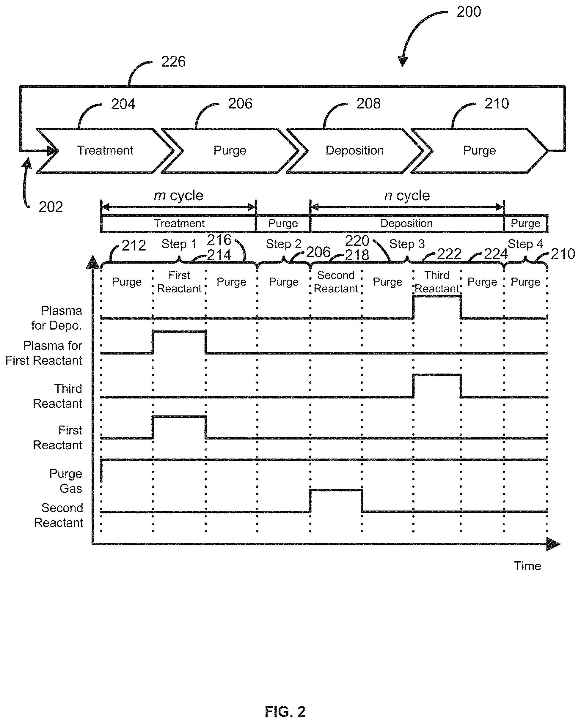
[0042] FIG. 2 illustrates a process sequence 200 in accordance with at least one embodiment of the disclosure. Process sequence 200 can be suitable for use with method of depositing a material on a surface of a substrate 100. FIG. 2 illustrates on/off sequences for gas flow and for plasma power or for provision of active species.
[0043] As illustrated, a deposition sequence 202 can include a treatment step 204, a purge step 206, a deposition cycle 208, and a final purge step 210. Treatment step 204 can be repeated m times, where m ranges from about 1 to about 5 and deposition cycle 208 can be repeated n times, where n ranges from about 1 to about 25. A ratio of m:n can range from, for example, 1:1, 1:3, 1:5, 1:10 or anywhere between such values. Further, deposition sequence 202 can be repeated a number of times (loop 226) until a desired thickness of material is deposited. A ratio of m:n can vary or remain the same for each iteration of loop 226.
[0044] Step 204 can be the same or similar to step 104 and can follow step 102. In the illustrated example, step 204 includes an optional initial purge step 212, introduction or formation of first active species 214, and first reactant purge step 216. As illustrated, the supply of purge gas can be continuous throughout process sequence 200. A gas for forming a first active species can be provided (e.g., only) during step 216 and the plasma power for forming the first active species can be activated (e.g., only) during step 214. Alternatively, the first reactant can be supplied during one or more (e.g., all) of steps 212-224 and 210, as described in more detail in connection with FIG. 3. Similarly, a third reactant can be supplied during one or more of steps 214-224 and 210, and only activated during step 222. Step 216 can be the same or similar to first reactant purge step described above.
[0045] During step 206, another first reactant purge step can be used to facilitate removal of any unwanted material remaining from step 204. A flowrate of a purge gas during step 206 can be the same as the first purge gas flowrate described above. A time for step 206 can range from about 1 to about 10 seconds or about 4 to about 6 seconds.
[0046] Step 208 can be the same or similar to step 106, described above. As illustrated, each deposition cycle can include introduction of a second reactant (step 218), a second reactant purge (step 220), forming second active species from a third reactant (step 222), and a third reactant purge (step 224). Steps 218-224 can be the same or similar to step 106 described above.
[0047] Process sequence 200 can include a final purge step 210. The flowrate of a purge gas during step 210 can be the same or similar to third reactant purge sub step described above. A time for step 210 can range from about 0.1 to about 10 seconds or about 1 to about 5 seconds.
[0048] Table 1 below illustrates exemplary temperatures, power, frequency, pressure, flowrates, and reactor conditions suitable for method 100 and/or process sequence 200. The ranges provided below illustrate examples of the disclose. Unless noted otherwise, the ranges are not meant to limit the scope of the disclosure.
TABLE-US-00001 TABLE 1 Exemplary Exemplary Unit Range Range Common Source One or more of a aminosilane silane, precursor aminosilane, a siloxane amine, a silazane amine, an iodosilane, and a chloride Sus temp .degree. C. 250-350 50-450 Wall .degree. C. 150-190 50-200 Flange .degree. C. 150-190 50-200 Source Temp .degree. C. 25-35 20-50 RF Power W 700-900 500-1000 RF frequency MHZ 13-30 13-30 Depo Pressure Torr 2-4 1-5 Step time Sec Source feeding: Source feeding: 0.2-0.4 0.1-0.5 Purge: Purge: 0.2-0.4 0.1-0.5 Plasma: Plasma: 0.2-0.4 0.1-0.5 Purge: Purge: 0.2-0.4 0.1-0.5 Purge Ar Sccm 3000-3500 1000-4000 O.sub.2 Sccm 600-800 400-1000 Carrier Ar Sccm 800-1200 500-1500 N2 Pressure Torr 2-4 1-5 Treatment Step time Sec Purge: Purge: 10-15 1.0-20.0 Plasma: Plasma: 8-12 1.0-20.0 Purge: Purge: 0.3-0.6 0.1-1.0 Purge Ar Sccm 3000-3500 1000-4000 N.sub.2 Sccm 3000-5000 Orifice full open Carrier Ar Sccm 800-1200 500-1500
[0049] FIG. 4 illustrates wet etch rate ratios of silicon oxide, e.g., formed according to method 100 and/or process sequence 200, in LAL 15 etchant for a period of 30 seconds. The removal rates are measured at a center and edge of a substrate for films formed according to process sequence 200. As illustrated, the higher the treatment to deposition ratio, the lower the wet etch rate of the deposited film. This indicates that higher-quality films can be formed using treatment to deposition ratios of between about 1:1 and about 1:10.
[0050] FIG. 5 illustrates material deposited--e.g., according to method 100 and/or process sequence 200 into a recess having a 20:1 aspect ratio. FIG. 5 shows that, while the seam is significantly reduced using a treatment step as described herein, a relatively small seam can form with a deposition: treatment cycle ratio of about 1:10, but that no seam is observed at ratios of 1:5, 1:3, or 1:1.
[0051] FIG. 3 illustrates another process sequence 300 in accordance with at least one embodiment of the disclosure. Method 100 can use process sequence 300 for depositing material on a surface of a substrate. Process sequence 300 is similar to process sequence 200, except process sequence 300 includes fewer purge steps, and includes a continuous flow of a first reactant. The continuous flow of the first reactant is thought to contribute to more stable process environment and to improve uniformity (e.g., composition and/or thickness) of the material deposited onto the substrate surface.
[0052] Similar to process sequence 200, process sequence 300 includes a deposition sequence 302 that includes a treatment step 304 and a deposition cycle/step 306. Unlike process sequence 200, process sequence 300 does not include a purge step 206 or a final purge 210. This allows process sequence 300 to be relatively short, which, in turn, allows for relatively rapid deposition of high-quality deposited material and high through-put, which can be used to, for example, fill a recess within a substrate surface. Treatment step 304 can be repeated m times, where m ranges from about 1 to about 5 and deposition cycle 208 can be repeated n times, where n ranges from about 1 to about 2. A ratio of m:n can range from, for example, 1:1, 1:3, 1:5, 1:10 or anywhere between such values. Further, deposition sequence 302 can be repeated a number of times (loop 308) until a desired thickness of material is deposited. A ratio of m:n can vary or remain the same for each iteration of loop 308.
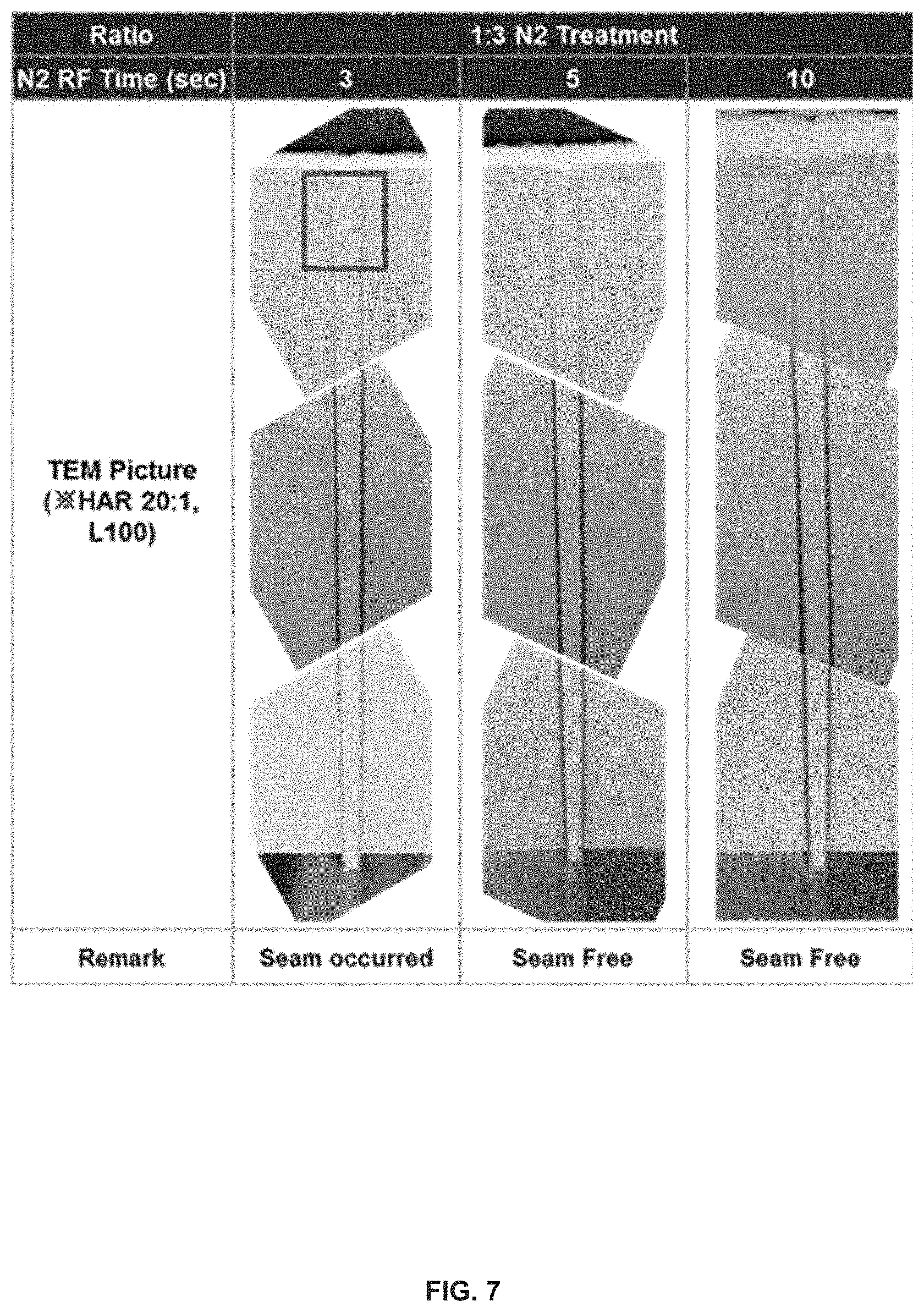
[0053] As illustrated in FIG. 3, process sequence 300 can begin with forming a first active species from a first reactant step 310, wherein a first reactant and a purge gas are continuously provided to a reaction chamber. During step 310, a first reactant may be activated by RF power to form first active species, as described above in connection with FIG. 1. A time for the plasma activation of the first reactant can range from greater than 3 seconds to about 10 (e.g., 5) seconds or about 4 seconds to about 8 seconds. Plasma ignition time is also thought to be an important factor for seamless fill of deposited material in a recess, and can depend on various factors, including an aspect ratio of a feature and a ration of m:n as defined above. For example, as illustrated in FIG. 7, for a m:n ratio of 1:3 and for a feature having an aspect ratio of 20:1, a plasma ignition time of less than 3 seconds in each treatment step may leave a seam in the deposited material. In the illustrative example, a plasma ignition time of five seconds or more in each treatment step did not result in seam formation in the deposited material. Thus, plasma ignition time may be based, at least in part, on aspect ratios of features on a surface of the substrate. During step 312, purge gas and first reactant are allowed to flow through the reaction chamber. Exemplary flowrates of purge gas and first reactant are provided below in Table 2.
[0054] During deposition cycle 306, a second reactant can be introduced to the reaction chamber. A flowrate of the second reactant and a pulse time for the second reactant can be the same or similar to the flowrate of the second reactant during steps 106 and 218, described above in connection with FIGS. 1 and 2. The second reactant can then be purged during step 316 by allowing the first reactant, the purge gas, and optionally the third reactant to continue to flow, as illustrated. When the third reactant is allowed to flow for additional steps (e.g., steps 312-316 and 320 in addition to step 318), the third reactant can be activated for a time period in step 318, such that second active species formed from the third reactant that react with the chemisorbed material to form deposited material is formed (e.g., only) during step 318. Alternatively, the third reactants can be flowed only during step 318. Exemplary power levels and times for activation of the third reactant are provided below in Table 2.
[0055] Table 2 below illustrates exemplary temperatures, power, frequency, pressure, flowrates, and reactor conditions suitable for method 100, process sequence 200 and/or process sequence 300. The ranges provided below illustrate examples of the disclose. Unless noted otherwise, the ranges are not meant to limit the scope of the disclosure.
TABLE-US-00002 TABLE 2 Exemplary Exemplary Unit Range Range Common Source One or more aminosilane of a silane, precursor aminosilane, a siloxane amine, a silazane amine, an iodosilane, and a chloride Substrate .degree. C. 250-350 50-450 temp Wall .degree. C. 150-190 50-200 Flange .degree. C. 150-190 50-200 Source Temp .degree. C. 25-35 20-50 RF Power W 700-900 500-1000 RF frequency MHZ 13-30 13-30 Depo Pressure Torr 2-4 1-5 Step time Sec Source feeding: Source feeding: 0.2-0.4 0.1-0.5 Purge: Purge: 0.2-0.4 0.1-0.5 Plasma: Plasma: 0.2-0.4 0.1-0.5 Purge: Purge: 0.1-0.3 0.1-0.5 Purge Ar Sccm 3000-3500 1000-4000 02 Sccm 600-800 400-1000 Carrier Ar Sccm 800-1200 500-1000 N.sub.2 Pressure Torr 2-4 1-5 Treatment Step time Sec Plasma: Plasma: 4.0-8.0 4.0-10.0 Purge: Purge: 0.2-0.6 0.1-1.0 Purge Ar Sccm 3000-3500 1000-4000 N.sub.2 Sccm 3000-5000 Orifice full open Carrier Ar Sccm 800-1000 500-1200
[0056] FIG. 6A and FIG. 6B illustrate a semiconductor processing apparatus 30 in accordance with exemplary embodiments of the disclosure. Semiconductor processing apparatus 30 includes one or more reaction chambers 3 for accommodating a substrate that can include a surface that can include a recess formed therein; a first source 21 for a first reactant in gas communication via a first valve 31 with one of the reaction chambers; a second source 22 for a second reactant in gas communication via a second valve 32 with one of the reaction chambers; a third source 25 for a third reactant in gas communication via a third valve 33 with one of the reaction chambers; an optional fourth source 26 (e.g., for a purge or carrier gas) in gas communication via a fourth valve 34 with one of the reaction chambers; and a controller 27 operably connected to the first, second, third, and optionally fourth gas valves and configured and programmed to control: forming first active species from a first reactant to modify a surface of the substrate and performing one or more deposition cycles to deposit material. Each deposition cycle can include introducing a second reactant to the substrate, wherein the second reactant reacts with the surface to form chemisorbed material; and forming second active species from a third reactant that react with the chemisorbed material to form deposited material. A ratio of a number of steps of forming first active species and a number of deposition cycles ranges from about 1:1 to about 1:10. The fourth gas can be introduced with any of the first, second, and/or third reactants, and/or can be used as a purge gas as described herein. Although not illustrated, semiconductor processing apparatus 30 can include additional sources and additional components, such as those typically found on semiconductor processing apparatus.
[0057] Optionally, semiconductor processing apparatus 30 is provided with a heater to activate the reactions by elevating the temperature of one or more of the substrate, the first, second and third reactants. Exemplary single wafer reactors, designed specifically to perform cyclic or ALD processes, are commercially available from ASM International NV (Almere, The Netherlands). Exemplary batch ALD reactors, designed specifically to perform ALD processes, are also commercially available from ASM International NV.
[0058] Semiconductor processing apparatus 30 may be provided with a radiofrequency source operably connected with the controller constructed and arranged to produce a plasma of at least one of the first, second and/or third reactant or combination of thereof. The plasma enhanced atomic layer deposition (PEALD) may be performed in a reactor available from ASM International NV of Almere, the Netherlands which apparatus comprises a plasma source to activate one or more of the reactants.
[0059] Process steps with a plasma may be performed using semiconductor processing apparatus 30, desirably in conjunction with controls programmed to conduct the sequences described herein, usable in at least some embodiments of the present disclosure. In the apparatus illustrated in FIG. 6A, by providing a pair of electrically conductive flat-plate electrodes 4, 2 in parallel and facing each other in the interior 11 (reaction zone) of reaction chamber 3, applying RF power (e.g., 13.56 MHz or 27 MHz) from a power source 20 to one side, and electrically grounding the other side 12, a plasma is excited between the electrodes.
[0060] A temperature regulator can be provided in a lower stage 2 (the lower electrode), and a temperature of substrate 1 placed thereon can be kept at a relatively constant temperature. The upper electrode 4 can serve as a shower plate as well, and reactant gas (and optionally an inert gas, such as a noble gas) and/or purge gasses can be introduced into the reaction chamber 3 through gas lines 41-44, respectively, and through the shower plate 4.
[0061] Additionally, in the reaction chamber 3, a circular duct 13 with an exhaust line 7 is provided, through which gas in the interior 11 of the reaction chamber 3 is exhausted. Additionally, a lower portion 5 of the reaction chamber 3--e.g., disposed below an upper portion 45 of the reaction chamber 3--is provided with a seal gas line 24 to introduce seal gas into the interior 11 of the reaction chamber 3 via the lower space 16 of the low portion 5 of the reaction chamber 3, wherein a separation plate 14 for separating the reaction zone between an upper electrode 4 and a lower stage 2 and the lower space 16 is provided (a gate valve through which a wafer is transferred into or from the lower portion of the reaction chamber 3 is omitted from this figure). The lower portion of the reaction chamber 5 is also provided with an exhaust line 6. In some embodiments, the deposition of a multi-element film and a surface treatment (e.g., steps 104-108) are performed in the same reaction space, so that all the steps can continuously be conducted without exposing the substrate to air or other oxygen-containing atmosphere. In some embodiments, a remote plasma unit can be used for exciting a gas--e.g., from one or more of sources 21, 22, 25, and/or 26.
[0062] In some embodiments, in the apparatus depicted in FIG. 6A, a system of switching flow of an inactive gas and flow of a precursor or reactant gas is illustrated in FIG. 6B; this system can be used to introduce the precursor or reactant gas in pulses without substantially fluctuating pressure of the reaction chamber. FIG. 6B illustrates a precursor supply system using a flow-pass system (FPS) according to an embodiment of the present disclosure (black valves indicate that the valves are closed). As shown in (a) in FIG. 6B, when feeding a precursor to a reaction chamber (not shown), first, a carrier gas such as Ar (or He) flows through a gas line with valves b and c, and then enters a bottle (reservoir) 20. The carrier gas flows out from the bottle 20 while carrying a precursor gas in an amount corresponding to a vapor pressure inside the bottle 20 and flows through a gas line with valves f and e, and is then fed to the reaction chamber together with the precursor. In this case, valves a and d are closed. When feeding only the carrier gas (e.g., noble gas) to the reaction chamber, as shown in (b) in FIG. 6B, the carrier gas flows through the gas line with the valve while bypassing the bottle 20. In this case, valves b, c, d, e, and f are closed. A reactant may be provided with the aid of a carrier gas.
[0063] A plasma for deposition may be generated in situ, for example, using one or more gasses that flow--e.g., continuously throughout the deposition cycle. In other embodiments, a plasma may be additionally or alternatively generated remotely and active species provided to the reaction chamber.
[0064] In some embodiments, a multi chamber reactor (more than two sections or compartments for processing wafers disposed closely to each other) can be used, wherein a reactant gas and an inert gas, such as a noble gas, can be supplied through a shared line, whereas a precursor gas can be supplied through unshared lines. Or a precursor gas can be supplied through shared lines.
[0065] An apparatus can include one or more controller(s), such as controller 27, programmed or otherwise configured to cause the deposition processes described herein to be conducted. The controller(s) can be communicated with the various power sources, heating systems, pumps, robotics, and gas flow controllers or valves of the reactor.
[0066] It is to be understood that the configurations and/or approaches described herein are exemplary in nature, and that these specific embodiments or examples are not to be considered in a limiting sense, because numerous variations are possible. The specific routines or methods described herein may represent one or more of any number of processing strategies. Thus, the various acts illustrated may be performed in the sequence illustrated, in other sequences, or omitted in some cases.
[0067] The subject matter of the present disclosure includes all novel and nonobvious combinations and sub-combinations of the various processes, systems, and configurations, and other features, functions, acts, and/or properties disclosed herein, as well as any and all equivalents thereof.
* * * * *
D00000
D00001
D00002
D00003
D00004
D00005
D00006
D00007
XML
uspto.report is an independent third-party trademark research tool that is not affiliated, endorsed, or sponsored by the United States Patent and Trademark Office (USPTO) or any other governmental organization. The information provided by uspto.report is based on publicly available data at the time of writing and is intended for informational purposes only.
While we strive to provide accurate and up-to-date information, we do not guarantee the accuracy, completeness, reliability, or suitability of the information displayed on this site. The use of this site is at your own risk. Any reliance you place on such information is therefore strictly at your own risk.
All official trademark data, including owner information, should be verified by visiting the official USPTO website at www.uspto.gov. This site is not intended to replace professional legal advice and should not be used as a substitute for consulting with a legal professional who is knowledgeable about trademark law.