Vacuum Transfer Device And A Method Of Forming The Same
A1
U.S. patent application number 16/272995 was filed with the patent office on 2020-08-13 for vacuum transfer device and a method of forming the same. The applicant listed for this patent is Prilit Optronics, Inc.. Invention is credited to Chun-Jen Weng, Biing-Seng Wu, Chao-Wen Wu.
| Application Number | 20200258767 16/272995 |
| Document ID | 20200258767 / US20200258767 |
| Family ID | 1000003939235 |
| Filed Date | 2020-08-13 |
| Patent Application | download [pdf] |


View All Diagrams
| United States Patent Application | 20200258767 |
| Kind Code | A1 |
| Wu; Biing-Seng ; et al. | August 13, 2020 |
VACUUM TRANSFER DEVICE AND A METHOD OF FORMING THE SAME
Abstract
A vacuum transfer device includes a semiconductor substrate, which has a first hole disposed in a top portion of the semiconductor substrate; a nozzle disposed in a bottom portion of the semiconductor substrate and protruding downward, the nozzle being aligned with the first hole; and a second hole disposed through the nozzle and in the semiconductor substrate to meet the first hole.
| Inventors: | Wu; Biing-Seng; (Tainan City, TW) ; Weng; Chun-Jen; (Tainan City, TW) ; Wu; Chao-Wen; (Tainan City, TW) | ||||||||||
| Applicant: |
|
||||||||||
|---|---|---|---|---|---|---|---|---|---|---|---|
| Family ID: | 1000003939235 | ||||||||||
| Appl. No.: | 16/272995 | ||||||||||
| Filed: | February 11, 2019 |
| Current U.S. Class: | 1/1 |
| Current CPC Class: | H01L 21/0337 20130101; H01L 33/005 20130101; B25J 15/0616 20130101; H01L 21/3086 20130101; H01L 21/6838 20130101 |
| International Class: | H01L 21/683 20060101 H01L021/683; B25J 15/06 20060101 B25J015/06 |
Claims
1. A method of forming a vacuum transfer device, comprising: providing a semiconductor substrate; forming a first mask layer on a top surface of the semiconductor substrate; etching the first mask layer to result in a pattern of a first hole through the first mask layer; etching the semiconductor substrate by using the first mask layer as an etch mask to make the first hole in a top portion of the semiconductor substrate; forming a second mask layer on a bottom surface of the semiconductor substrate; etching the second mask layer to result in a pattern defining a nozzle aligned with the first hole; etching the semiconductor substrate by using the second mask layer as an etch mask to make the nozzle in a bottom portion of the semiconductor substrate and protruding downward; forming a third mask layer on the bottom surface of the semiconductor substrate; etching the second mask layer to result in a pattern of a second hole through the second mask layer; and etching the semiconductor substrate by using the second mask layer and the third mask layer as an etch mask to make the second hole through the nozzle and in the semiconductor substrate to meet the first hole.
2. The method of claim 1, wherein the first mask layer, the second mask layer or the third mask layer comprises silicon nitride, silicon oxide or metal.
3. The method of claim 1, further comprising: removing the first mask layer after the step of etching the semiconductor substrate to make the first hole therein.
4. The method of claim 1, wherein the nozzle is at least partially overlapped with the first hole.
5. The method of claim 1, wherein the nozzle has a dimension smaller than the first hole.
6. The method of claim 1, wherein the second hole is at least partially overlapped with the nozzle and the first hole.
7. The method of claim 1, wherein the second hole has a dimension smaller than the nozzle.
8. The method of claim 1, further comprising: removing the second mask layer and the third mask layer after the step of etching the semiconductor substrate to make the second hole in the semiconductor substrate.
9. The method of claim 1, further comprising: providing an adaptor that holds the top surface of the semiconductor substrate; wherein the adaptor has a vacuum channel through the adaptor and communicating with the first hole.
10. The method of claim 9, wherein the adaptor has a plurality of peripheral channels through the adaptor and located on a periphery of the adaptor.
11. The method of claim 9, further comprising a step of fastening the adaptor and the semiconductor substrate by a clamp.
12. A vacuum transfer device, comprising: a semiconductor substrate having: a first hole disposed in a top portion of the semiconductor substrate; a nozzle disposed in a bottom portion of the semiconductor substrate and protruding downward, the nozzle being aligned with the first hole; and a second hole disposed through the nozzle and in the semiconductor substrate to meet the first hole.
13. The device of claim 12, wherein the nozzle is at least partially overlapped with the first hole.
14. The device of claim 12, wherein the nozzle has a dimension smaller than the first hole.
15. The device of claim 12, wherein the second hole is at least partially overlapped with the nozzle and the first hole.
16. The device of claim 12, wherein the second hole has a dimension smaller than the nozzle.
17. The device of claim 12, further comprising: a first mask layer disposed on a top surface of the semiconductor substrate but not covering the first hole.
18. The device of claim 17, further comprising: a second mask layer disposed on a bottom surface of the nozzle but not covering the second hole; and a third mask layer disposed on a bottom surface of the semiconductor substrate but not covering the nozzle.
19. The device of claim 18, wherein the first mask layer, the second mask layer or the third mask layer comprises silicon nitride, silicon oxide or metal.
20. The device of claim 12, further comprising: an adaptor that holds a top surface of the semiconductor substrate; wherein the adaptor has a vacuum channel through the adaptor and communicating with the first hole.
21. The device of claim 20, wherein the adaptor has a plurality of peripheral channels through the adaptor and located on a periphery of the adaptor.
22. The device of claim 20, further comprising a clamp that fastens the adaptor and the semiconductor substrate.
Description
BACKGROUND OF THE INVENTION
1. Field of the Invention
[0001] The present invention generally relates to a micro light-emitting diode (microLED), and more particularly to a method of forming a vacuum transfer device adaptable to transferring the microLED.
2. Description of Related Art
[0002] A micro light-emitting diode (microLED, mLED or .mu.LED) display panel is one of flat display panels, and is composed of microscopic microLEDs each having a size of 1-10 micrometers. Compared to conventional liquid crystal display panels, the microLED display panels offer better contrast, response time and energy efficiency. Although both organic light-emitting diodes (OLEDs) and microLEDs possess good energy efficiency, the microLEDs, based on group III/V (e.g., GaN) LED technology, offer higher brightness, higher luminous efficacy and longer lifespan than the OLEDs.
[0003] During manufacturing a microLED display panel, individual microLEDs should be picked up and transferred to a display panel, for example, by vacuum suction force. Conventional vacuum transfer devices are usually manufactured by laser or electromagnetic technique, which requires substantial working time and high cost, and therefore cannot be adapted to large-size or high-resolution display panels.
[0004] A need has thus arisen to propose a novel vacuum transfer device to overcome deficiency of conventional transfer devices.
SUMMARY OF THE INVENTION
[0005] In view of the foregoing, it is an object of the embodiment of the present invention to provide a method of forming a vacuum transfer device adaptable to transferring a micro device such as a micro light-emitting diode (microLED) in an economic and simple manner by using semiconductor device fabrication technique.
[0006] According to one embodiment, a method of forming a vacuum transfer device mainly includes the following steps. A first mask layer is formed on a top surface of a semiconductor substrate, and is etched to result in a pattern of a first hole through the first mask layer. The semiconductor substrate is etched by using the first mask layer as an etch mask to make the first hole in a top portion of the semiconductor substrate. A second mask layer is formed on a bottom surface of the semiconductor substrate, and is etched to result in a pattern defining a nozzle aligned with the first hole. The semiconductor substrate is etched by using the second mask layer as an etch mask to make the nozzle in a bottom portion of the semiconductor substrate and protruding downward. A third mask layer is formed on the bottom surface of the semiconductor substrate. The second mask layer is etched to result in a pattern of a second hole through the second mask layer. The semiconductor substrate is etched by using the second mask layer and the third mask layer as an etch mask to make the second hole through the nozzle and in the semiconductor substrate to meet the first hole.
BRIEF DESCRIPTION OF THE DRAWINGS
[0007] FIG. 1A to FIG. 1K show cross-sectional views illustrating a method of forming a vacuum transfer device adaptable to transferring a micro device according to one embodiment of the present invention;
[0008] FIG. 2A to FIG. 2K show cross-sectional views illustrating a method of forming a vacuum transfer device adaptable to transferring a micro device according to another embodiment of the present invention;
[0009] FIG. 3A shows a cross-sectional view illustrating an array of vacuum transfer devices performed by dry etching only;
[0010] FIG. 3B shows a cross-sectional view illustrating an array of vacuum transfer devices performed by wet and dry etching;
[0011] FIG. 4A shows a cross-sectional view illustrating an array of vacuum transfer devices performed by dry etching only; and
[0012] FIG. 4B shows a cross-sectional view illustrating an array of vacuum transfer devices performed by wet and dry etching.
DETAILED DESCRIPTION OF THE INVENTION
[0013] FIG. 1A to FIG. 1K show cross-sectional views illustrating a method of forming a vacuum transfer device adaptable to transferring a micro device such as a micro light-emitting diode (microLED) according to one embodiment of the present invention. A plurality of vacuum transfer devices may be formed simultaneously to form a vacuum transfer array.
[0014] Referring to FIG. 1A, a semiconductor substrate 11 is provided. The semiconductor substrate 11 of the embodiment may, for example, be composed of silicon. A first mask layer 12 is formed on a top surface of the semiconductor substrate 11. The first mask layer 12 of the embodiment is a hardmask that acts as an etch mask in the following process steps. The first mask layer 12 of the embodiment may include, for example, silicon nitride Si.sub.3N.sub.4, silicon oxide SiO.sub.2 or metal. A first photoresist (PR) layer 13 with a pattern defining a first hole (or holes) 131 is formed on the first mask layer 12. After the first photoresist layer 13 is subjected to photolithographic process (e.g., exposure and developing), the first mask layer 12 is etched by using the first photoresist layer 13 as an etch mask, thereby resulting in the first mask layer 12 with the pattern of the first hole 131 (vertically) through the first mask layer 12 as shown in FIG. 1B.
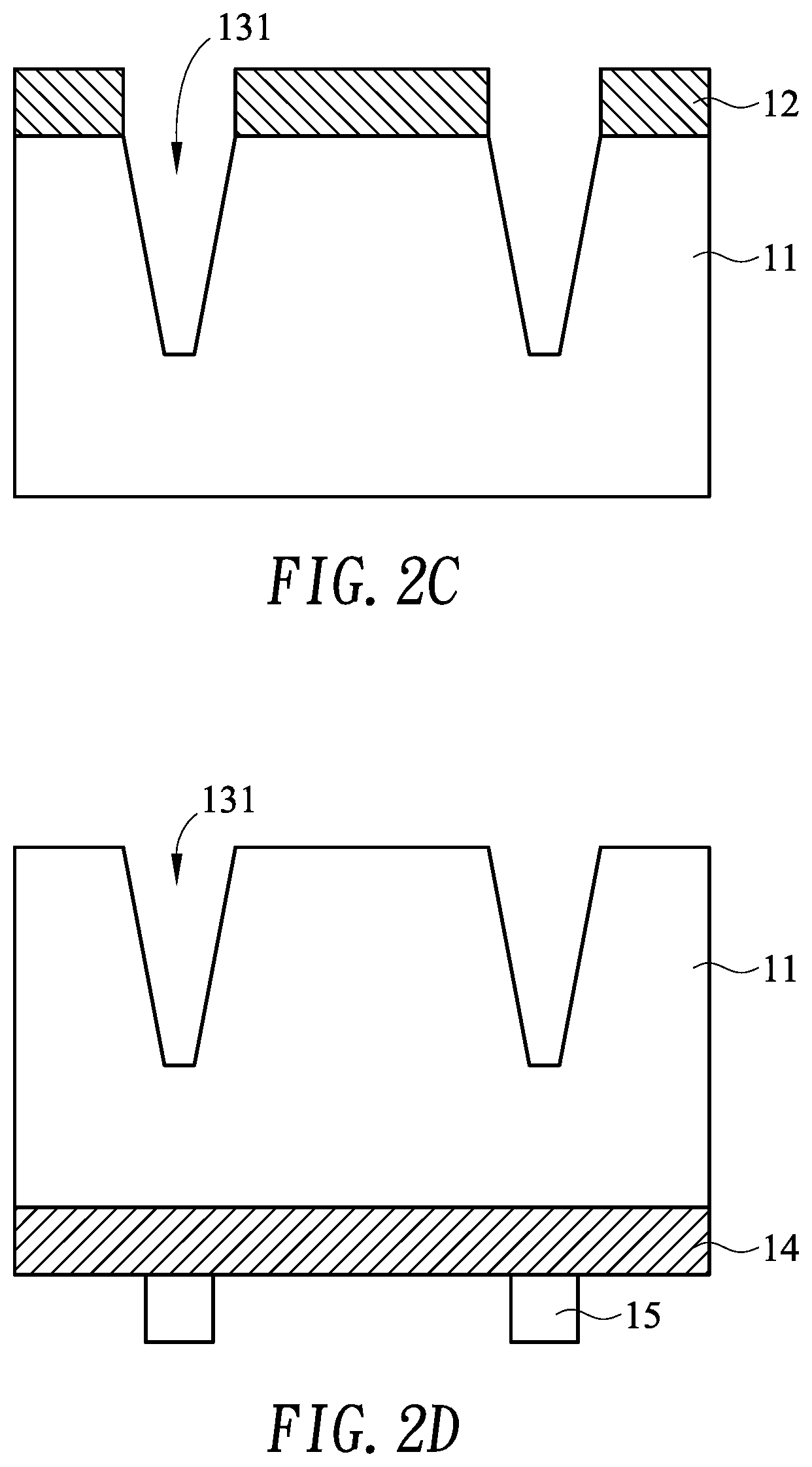
[0015] Referring to FIG. 1C, the semiconductor substrate 11 is etched (e.g., by dry etching) by using the first mask layer 12 as an etch mask to make the first hole 131 in a top portion of (but not through) the semiconductor substrate 11. The first mask layer 12 is then removed. In another embodiment, the first mask layer 12 remains on the semiconductor substrate 11 without being removed.
[0016] Referring to FIG. 1D, a second mask layer 14 is formed on a bottom surface of the semiconductor substrate 11. The second mask layer 14 of the embodiment is a hardmask that acts as an etch mask in the following process steps. The second mask layer 14 of the embodiment may include, for example, silicon nitride Si.sub.3N.sub.4, silicon oxide SiO.sub.2 or metal. A second photoresist (PR) layer 15 with a pattern defining a nozzle (or nozzles) 151 aligned with the first hole 131 is formed on the second mask layer 14. After the second photoresist layer 15 is subjected to photolithographic process (e.g., exposure and developing), the second mask layer 14 is etched by using the second photoresist layer 15 as an etch mask, thereby resulting in the second mask layer 14 with the pattern of the nozzle 151 as shown in FIG. 1E.
[0017] Referring to FIG. 1F, the semiconductor substrate 11 is etched (e.g., by dry etching) by using the second mask layer 14 as an etch mask to make the nozzle 151 in a bottom portion of the semiconductor substrate 11 and protruding downward. In the embodiment, the nozzle 151 may be aligned with, and at least partially overlapped with the first hole 131. The nozzle 151 may have a dimension (e.g., width) smaller than the first hole 131.
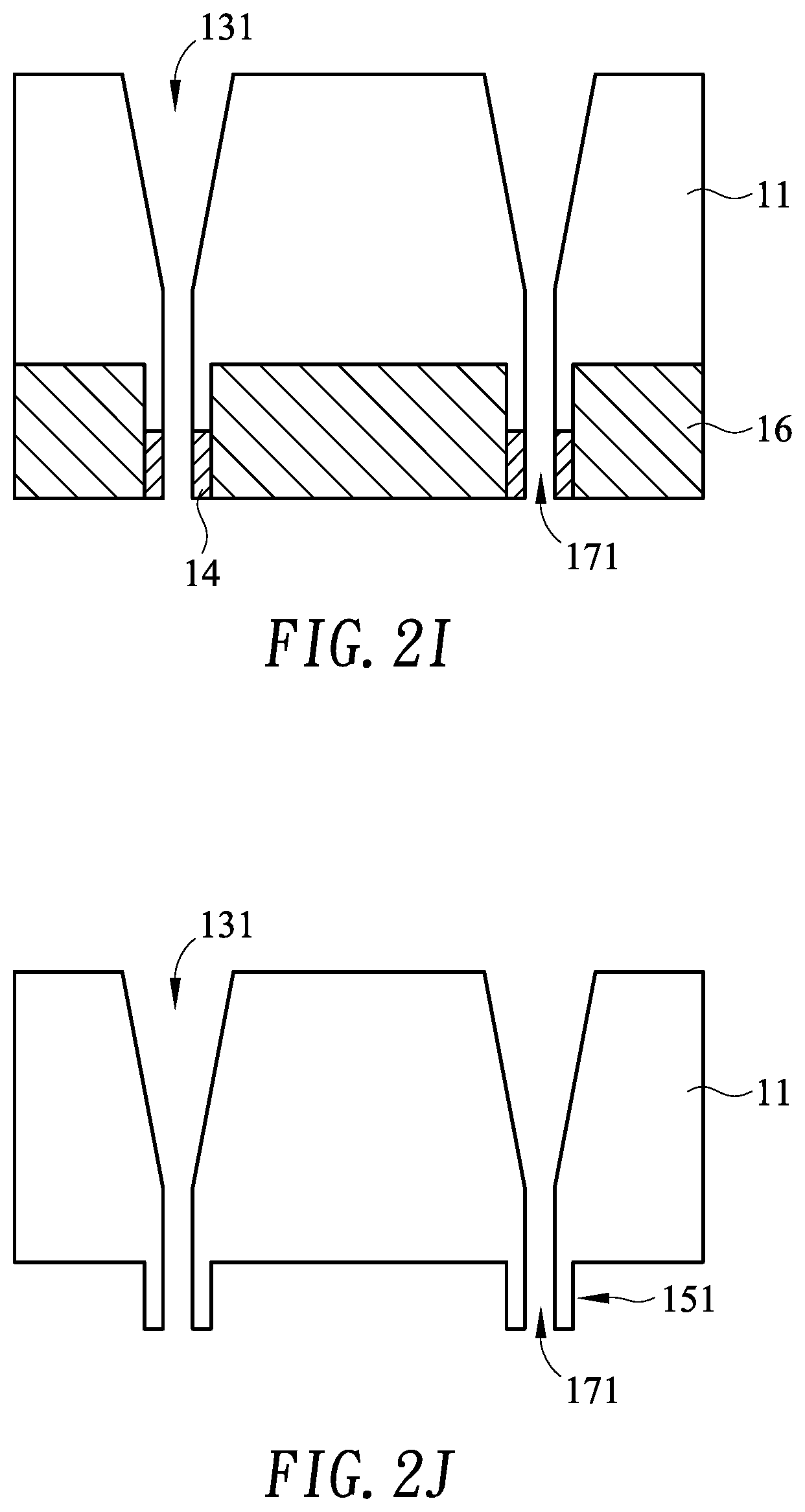
[0018] Referring to FIG. 1G, a third mask layer 16 is formed on a bottom surface of the semiconductor substrate 11. The third mask layer 16 of the embodiment is a hardmask that acts as an etch mask in the following process steps. The third mask layer 16 of the embodiment may include, for example, silicon nitride Si.sub.3N.sub.4, silicon oxide SiO.sub.2 or metal. A third photoresist (PR) layer 17 with a pattern defining a second hole (or holes) 171 aligned with the nozzle 151 and the first hole 131 is formed on the second mask layer 14 and the third mask layer 16. After the third photoresist layer 17 is subjected to photolithographic process (e.g., exposure and developing), the second mask layer 14 and the third mask layer 16 are etched by using the third photoresist layer 17 as an etch mask, thereby resulting in the second mask layer 14 with the pattern of the second hole 171 (vertically) through the nozzle 151 as shown in FIG. 1H.
[0019] Referring to FIG. 1I, the semiconductor substrate 11 is etched by using the second mask layer 14 and the third mask layer 16 as an etch mask to make the second hole 171 in and (vertically) through the nozzle 151 and in the semiconductor substrate 11 to meet (i.e., communicate with) the first hole 131. In the embodiment, the second hole 171 may be aligned with, and at least partially overlapped with the nozzle 151 and the first hole 131. The second hole 171 may have a dimension (e.g., width) smaller than the nozzle 151. In one embodiment, the dimension (e.g., width) of the second hole 171 may be less than or equal to 100 micrometers.
[0020] Referring to FIG. 1J, the second mask layer 14 and the third mask layer 16 are then removed. In another embodiment, the second mask layer 14 and the third mask layer 16 remain on the semiconductor substrate 11 without being removed.
[0021] Referring to FIG. 1K, an adaptor 18 may hold (e.g., suck) the top surface of the semiconductor substrate 11 by vacuum force. The adaptor 18 may have a vacuum channel 181 (vertically) through the adaptor 18. The vacuum channel 181 may communicate with the first hole 131 and the second hole 171 (in the semiconductor substrate 11). In the specific embodiment shown in FIG. 1K, one vacuum channel 181 is associated with plural (e.g., two) first holes 131.
[0022] In the embodiment discussed above, the process associated with FIG. 1C is performed by dry etching only. FIG. 2A to FIG. 2K show cross-sectional views illustrating a method of forming a vacuum transfer device by wet and dry etching adaptable to transferring a micro device such as a micro light-emitting diode (microLED) according to another embodiment of the present invention. In this embodiment, the process associated with FIG. 2C is performed by wet etching.
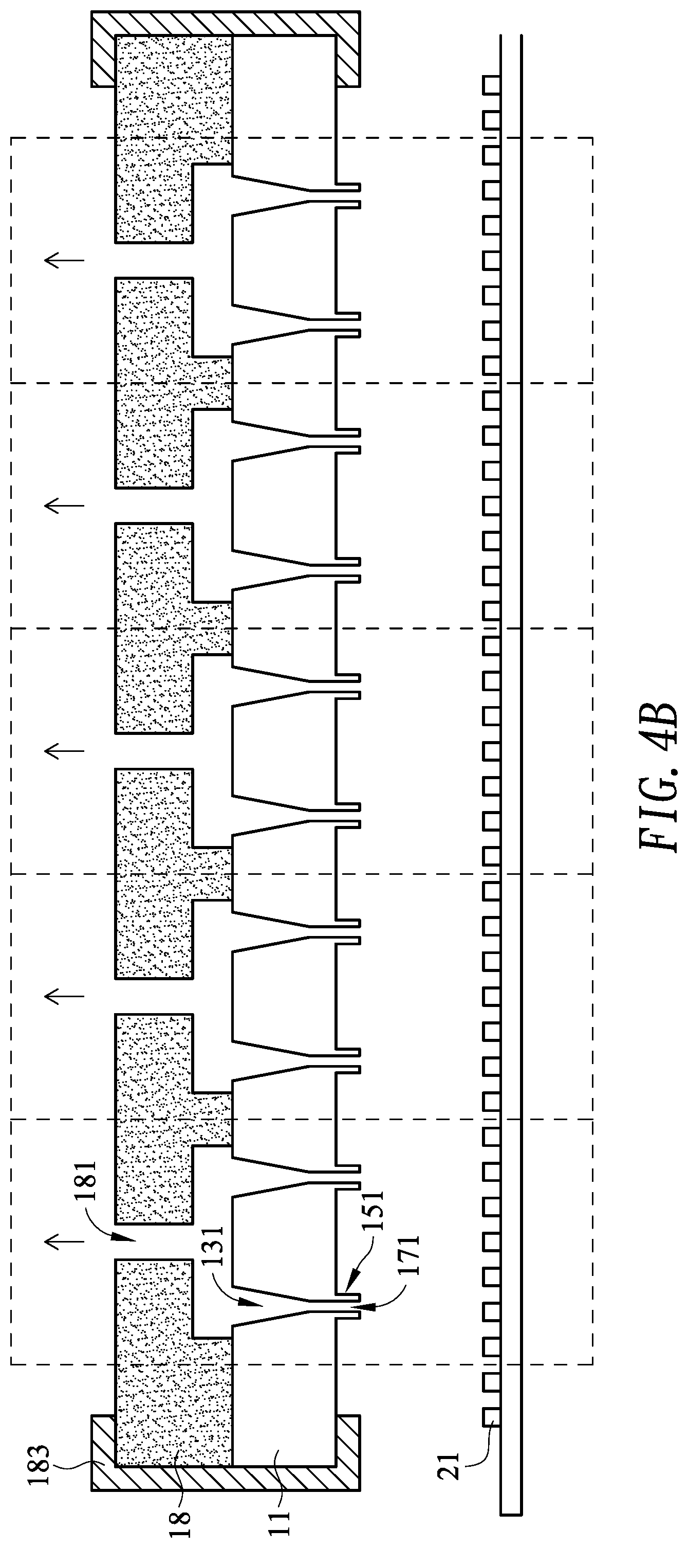
[0023] FIG. 3A shows a cross-sectional view illustrating an array of vacuum transfer devices (i.e., a vacuum transfer array) performed by dry etching only, and FIG. 3B shows a cross-sectional view illustrating an array of vacuum transfer devices performed by wet and dry etching. When air is being pumped out through a top opening of the vacuum channel 181, vacuum is generated therein and microLEDs 21 (disposed on an LED substrate) may be sucked at a bottom opening of the second hole 171 (of the nozzle 151) and ready to be placed, for example, on a display substrate. The microLEDs 21 may be released when the air pumping stops.
[0024] In the embodiment, the adaptor 18 may have a plurality of peripheral channels 182 (vertically) through the adaptor 18 and located on a periphery of the adaptor 18. When air is being pumped out through a top opening of the peripheral channel 182, vacuum is generated therein and the semiconductor substrate 11 may be sucked at a bottom opening of the peripheral channel 182. The semiconductor substrate 11 may be released when the air pumping stops.
[0025] In another embodiment, as shown in FIG. 4A which illustrates an array of vacuum transfer devices performed by dry etching only, or as shown in FIG. 4B which illustrates an array of vacuum transfer devices performed by dry and wet etching, a clamp 183 may be further provided to fasten the adaptor 18 and the semiconductor substrate 11 by mechanical mechanism.
[0026] According to the embodiment as set forth above, an economic and fast scheme has been proposed to make an array of vacuum transfer device adaptable to transferring a microLED. The proposed scheme may be well adaptable to large-size or high-resolution microLED display panel. Moreover, the proposed scheme is scalable and is capable of increasing or decreasing the size of the array of vacuum transfer device according to requirement.
[0027] Although specific embodiments have been illustrated and described, it will be appreciated by those skilled in the art that various modifications may be made without departing from the scope of the present invention, which is intended to be limited solely by the appended claims.
* * * * *
D00000
D00001
D00002
D00003
D00004
D00005
D00006
D00007
D00008
D00009
D00010
D00011
D00012

D00013

D00014

D00015

D00016
XML
uspto.report is an independent third-party trademark research tool that is not affiliated, endorsed, or sponsored by the United States Patent and Trademark Office (USPTO) or any other governmental organization. The information provided by uspto.report is based on publicly available data at the time of writing and is intended for informational purposes only.
While we strive to provide accurate and up-to-date information, we do not guarantee the accuracy, completeness, reliability, or suitability of the information displayed on this site. The use of this site is at your own risk. Any reliance you place on such information is therefore strictly at your own risk.
All official trademark data, including owner information, should be verified by visiting the official USPTO website at www.uspto.gov. This site is not intended to replace professional legal advice and should not be used as a substitute for consulting with a legal professional who is knowledgeable about trademark law.