Semiconductor Substrate, And Epitaxial Wafer And Method For Producing Same
GOTO; Ken ; et al.
U.S. patent application number 16/061486 was filed with the patent office on 2020-07-30 for semiconductor substrate, and epitaxial wafer and method for producing same. This patent application is currently assigned to TAMURA CORPORATION. The applicant listed for this patent is TAMURA CORPORATION National Unversity Corporation Tokyo University of Agriculture and Technology. Invention is credited to Ken GOTO, Yoshinao KUMAGAI, Hisashi MURAKAMI.
| Application Number | 20200243332 16/061486 |
| Document ID | 20200243332 / |
| Family ID | 1000004824847 |
| Filed Date | 2020-07-30 |


View All Diagrams
| United States Patent Application | 20200243332 |
| Kind Code | A1 |
| GOTO; Ken ; et al. | July 30, 2020 |
SEMICONDUCTOR SUBSTRATE, AND EPITAXIAL WAFER AND METHOD FOR PRODUCING SAME
Abstract
A semiconductor substrate that is used as an underlying substrate for epitaxial crystal growth carried out by the HVPE method includes a .beta.-Ga.sub.2O.sub.3-based single crystal, and a principal plane that is a plane parallel to a [100] axis of the .beta.-Ga.sub.2O.sub.3-based single crystal. An epitaxial wafer includes the semiconductor substrate, and an epitaxial layer including a .beta.-Ga.sub.2O.sub.3-based single crystal and formed on the principal plane of the semiconductor substrate by epitaxial crystal growth using the HVPE method. A method for producing an epitaxial wafer includes by using the HVPE method, epitaxially growing an epitaxial layer including a .beta.-Ga.sub.2O.sub.3-based single crystal on a semiconductor substrate that includes a .beta.-Ga.sub.2O.sub.3-based single crystal and has a principal plane parallel to a [100] axis of the .beta.-Ga.sub.2O.sub.3-based single crystal.
| Inventors: | GOTO; Ken; (Tokyo, JP) ; KUMAGAI; Yoshinao; (Tokyo, JP) ; MURAKAMI; Hisashi; (Tokyo, JP) | ||||||||||
| Applicant: |
|
||||||||||
|---|---|---|---|---|---|---|---|---|---|---|---|
| Assignee: | TAMURA CORPORATION Tokyo JP National University Corporation Tokyo University of Agriculture and Technology Tokyo JP |
||||||||||
| Family ID: | 1000004824847 | ||||||||||
| Appl. No.: | 16/061486 | ||||||||||
| Filed: | November 16, 2016 | ||||||||||
| PCT Filed: | November 16, 2016 | ||||||||||
| PCT NO: | PCT/JP2016/083986 | ||||||||||
| 371 Date: | June 12, 2018 |
| Current U.S. Class: | 1/1 |
| Current CPC Class: | C30B 25/20 20130101; H01L 21/02293 20130101; H01L 21/02631 20130101; C30B 25/16 20130101; H01L 21/02609 20130101; C30B 29/16 20130101 |
| International Class: | H01L 21/02 20060101 H01L021/02; C30B 29/16 20060101 C30B029/16; C30B 25/20 20060101 C30B025/20; C30B 25/16 20060101 C30B025/16 |
Foreign Application Data
| Date | Code | Application Number |
|---|---|---|
| Dec 16, 2015 | JP | 2015-245570 |
Claims
1. A semiconductor substrate that is used as an underlying substrate for epitaxial crystal growth carried out by the HVPE method, the semiconductor substrate comprising: a .beta.Ga.sub.2O.sub.3-based single crystal; and a principal plane that is a plane parallel to a [100] axis of the .beta.-Ga.sub.2O.sub.3-based single crystal.
2. The semiconductor substrate according to claim 1, wherein an angle .theta. formed between the principal plane and a (001) plane of the .beta.-Ga.sub.2O.sub.3-based single crystal is not less than 30.degree. and not more than 90.degree., or not less than -150.degree. and not more than -90.degree., where an angle generated by rotation in a rotation direction of a right-handed screw advancing in the a-axis direction is defined as a positive angle.
3. The semiconductor substrate according to claim 2, wherein the semiconductor substrate has an average dislocation density of not more than 1.times.10.sup.4/cm.sup.2, and the angle .theta. is not less than 54.3.degree. and not more than 65.7.degree., or not less than -125.7.degree. and not more than -114.3.degree..
4. The semiconductor substrate according to claim 2, wherein the semiconductor substrate has an average dislocation density of not more than 1.times.10.sup.3/cm.sup.2, and the angle .theta. is not less than 41.6.degree. and not more than 78.4.degree., or not less than -138.4.degree. and not more than -101.6.degree..
5. The semiconductor substrate according to claim 1, wherein an angle .theta. formed between the principal plane and the (001) plane of the .beta.-Ga.sub.2O.sub.3-based single crystal is not less than -0.33.degree. and not more than 0.33.degree., more than 45.degree. and not more than 90.degree., or less than -45.degree. and not less than -90.degree., where an angle generated by rotation in a rotation direction of a right-handed screw advancing in the a-axis direction is defined as a positive angle.
6. The semiconductor substrate according to claim 1, wherein an angle .theta. formed between the principal plane and the (001) plane of the .beta.-Ga.sub.2O.sub.3-based single crystal is not less than -30.degree. and not more than 30.degree., where an angle generated by rotation in a rotation direction of a right-handed screw advancing in the a-axis direction is defined as a positive angle.
7. The semiconductor substrate according to claim 6, wherein the angle .theta. is not less than 0.3.degree. and not more than 15.degree., or not less than -15.degree. and not more than -0.3.degree..
8. An epitaxial wafer, comprising: the semiconductor substrate according to claim 1; and an epitaxial layer comprising a .beta.-Ga.sub.2O.sub.3-based single crystal and formed on the principal plane of the semiconductor substrate by epitaxial crystal growth using the HVPE method.
9. A method for producing an epitaxial wafer, comprising: by using the HVPE method, epitaxially growing an epitaxial layer comprising a .beta.-Ga.sub.2O.sub.3-based single crystal on a semiconductor substrate that comprises a .beta.-Ga.sub.2O.sub.3-based single crystal and has a principal plane parallel to a [100] axis of the .beta.-Ga.sub.2O.sub.3-based single crystal.
10. The method for producing an epitaxial wafer according to claim 9, wherein an angle .theta. formed between the principal plane and a (001) plane of the .beta.-Ga.sub.2O.sub.3-based single crystal is not less than 30.degree. and not more than 90.degree., or not less than -150.degree. and not more than -90.degree., where an angle generated by rotation in a rotation direction of a right-handed screw advancing in the a-axis direction is defined as a positive angle.
11. The method for producing an epitaxial wafer according to claim 10, wherein the semiconductor substrate has an average dislocation density of not more than 1.times.10.sup.4/cm.sup.2, and the angle .theta. is not less than 54.3.degree. and not more than 65.7.degree., or not less than -125.7.degree. and not more than -114.3.degree..
12. The method for producing an epitaxial wafer according to claim 10, wherein the semiconductor substrate has an average dislocation density of not more than 1.times.10.sup.3/cm.sup.2, and the angle .theta. is not less than 41.6.degree. and not more than 78.4.degree., or not less than -138.4.degree. and not more than -101.6.degree..
13. The method for producing an epitaxial wafer according to claim 9, wherein an angle .theta. formed between the principal plane and the (001) plane of the .beta.-Ga.sub.2O.sub.3-based single crystal is not less than -0.33.degree. and not more than 0.33.degree., more than 45.degree. and not more than 90.degree., or less than -45.degree. and not less than -90.degree., where an angle generated by rotation in a rotation direction of a right-handed screw advancing in the a-axis direction is defined as a positive angle.
14. The method for producing an epitaxial wafer according to claim 9, wherein the growth rate of the epitaxial layer is not less than 2.5 .mu.m/h.
15. The method for producing an epitaxial wafer according to claim 14, wherein an angle .theta. formed between the principal plane and the (001) plane of the .beta.-Ga.sub.2O.sub.3-based single crystal is not less than -30.degree. and not more than 30.degree., where an angle generated by rotation in a rotation direction of a right-handed screw advancing in the a-axis direction is defined as a positive angle.
16. The method for producing an epitaxial wafer according to claim 15, wherein the angle .theta. is not less than 0.3.degree. and not more than 15.degree., or not less than -15.degree. and not more than -0.3.degree..
Description
TECHNICAL FIELD
[0001] The invention relates to a semiconductor substrate, and an epitaxial wafer and a method for manufacturing the same.
BACKGROUND ART
[0002] A technique of forming a .beta.-Ga.sub.2O.sub.3 single crystal film on a .beta.-Ga.sub.2O.sub.3-based substrate by epitaxial crystal growth using the MBE (Molecular Beam Epitaxy) method is conventionally known (see, e.g., WO 2013/035464).
[0003] According to WO 2013/035464, the .beta.-Ga.sub.2O.sub.3 single crystal film can be grown at a high growth rate by the MBE method when the plane orientation of the principal plane of the .beta.-Ga.sub.2O.sub.3-based substrate is adjusted to a predetermined plane orientation.
CITATION LIST
Patent Literatures
WO 2013/035464
SUMMARY OF INVENTION
Technical Problem
[0004] It is an object of the invention to provide a semiconductor substrate comprising a .beta.-Ga.sub.2O.sub.3-based single crystal on which an epitaxial layer comprising a .beta.-Ga.sub.2O.sub.3-based single crystal can be grown by the HVPE method at a high growth rate; an epitaxial wafer having the semiconductor substrate and an epitaxial layer; and a method for producing the epitaxial wafer.
[0005] It is another object of the invention to provide a semiconductor substrate comprising a .beta.-Ga.sub.2O.sub.3-based single crystal on which an epitaxial layer comprising a .beta.-Ga.sub.2O.sub.3-based single crystal having good surface morphology can be grown by the HVPE method; an epitaxial wafer having the semiconductor substrate and an epitaxial layer; and a method for producing the epitaxial wafer.
Solution to Problem
[0006] To achieve the above-mentioned objects, an aspect of the invention provides a semiconductor substrate described in [1] to [7] below, an epitaxial wafer described in [8], or a method for producing an epitaxial wafer described in [9] to [16].
[0007] [1] A semiconductor substrate that is used as an underlying substrate for epitaxial crystal growth carried out by the HVPE method, the semiconductor substrate comprising: a .beta.-Ga.sub.2O.sub.3-based single crystal; and a principal plane that is a plane parallel to a [100] axis of the .beta.-Ga.sub.2O.sub.3-based single crystal.
[0008] [2] The semiconductor substrate described in [1], wherein an angle .theta. formed between the principal plane and a (001) plane of the .beta.-Ga.sub.2O.sub.3-based single crystal is not less than 30.degree. and not more than 90.degree., or not less than -150.degree. and not more than -90.degree., where an angle generated by rotation in a rotation direction of a right-handed screw advancing in the a-axis direction is defined as a positive angle.
[0009] [3] The semiconductor substrate described in [2], wherein the semiconductor substrate has an average dislocation density of not more than 1.times.10.sup.4/cm.sup.2, and the angle .theta. is not less than 54.3.degree. and not more than 65.7.degree., or not less than -125.7.degree. and not more than -114.3.degree..
[0010] [4] The semiconductor substrate described in [2], wherein the semiconductor substrate has an average dislocation density of not more than 1.times.10.sup.3/cm.sup.2, and the angle .theta. is not less than 41.6.degree. and not more than 78.4.degree., or not less than -138.4.degree. and not more than -101.6.degree..
[0011] [5] The semiconductor substrate described in [1], wherein an angle .theta. formed between the principal plane and the (001) plane of the .beta.-Ga.sub.2O.sub.3-based single crystal is not less than -0.33.degree. and not more than 0.33.degree., more than 45.degree. and not more than 90.degree., or less than -45.degree. and not less than -90.degree., where an angle generated by rotation in a rotation direction of a right-handed screw advancing in the a-axis direction is defined as a positive angle.
[0012] [6] The semiconductor substrate described in [1], wherein an angle .theta. formed between the principal plane and the (001) plane of the .beta.-Ga.sub.2O.sub.3-based single crystal is not less than -30.degree. and not more than 30.degree., where an angle generated by rotation in a rotation direction of a right-handed screw advancing in the a-axis direction is defined as a positive angle.
[0013] [7] The semiconductor substrate described in [6], wherein the angle .theta. is not less than 0.3.degree. and not more than 15.degree., or not less than -15.degree. and not more than -0.3.degree..
[0014] [8] An epitaxial wafer, comprising: the semiconductor substrate described in any one of [1] to [7]; and an epitaxial layer comprising a .beta.-Ga.sub.2O.sub.3-based single crystal and formed on the principal plane of the semiconductor substrate by epitaxial crystal growth using the HVPE method.
[0015] [9] A method for producing an epitaxial wafer, comprising: by using the HVPE method, epitaxially growing an epitaxial layer comprising a .beta.-Ga.sub.2O.sub.3-based single crystal on a semiconductor substrate that comprises a .beta.-Ga.sub.2O.sub.3-based single crystal and has a principal plane parallel to a [100] axis of the .beta.-Ga.sub.2O.sub.3-based single crystal.
[0016] [10] The method for producing an epitaxial wafer described in [9], wherein an angle .theta. formed between the principal plane and a (001) plane of the .beta.-Ga.sub.2O.sub.3-based single crystal is not less than 30.degree. and not more than 90.degree., or not less than -150.degree. and not more than -90.degree., where an angle generated by rotation in a rotation direction of a right-handed screw advancing in the a-axis direction is defined as a positive angle.
[0017] [11] The method for producing an epitaxial wafer described in [10], wherein the semiconductor substrate has an average dislocation density of not more than 1.times.10.sup.4/cm.sup.2, and the angle .theta. is not less than 54.3.degree. and not more than 65.7.degree., or not less than -125.7.degree. and not more than -114.3.degree..
[0018] [12] The method for producing an epitaxial wafer described in [10], wherein the semiconductor substrate has an average dislocation density of not more than 1.times.10.sup.3/cm.sup.2, and the angle .theta. is not less than 41.6.degree. and not more than 78.4.degree., or not less than -138.4.degree. and not more than -101.6.degree..
[0019] [13] The method for producing an epitaxial wafer described in [9], wherein an angle .theta. formed between the principal plane and the (001) plane of the .beta.-Ga.sub.2O.sub.3-based single crystal is not less than -0.33.degree. and not more than 0.33.degree., more than 45.degree. and not more than 90.degree., or less than -45.degree. and not less than -90.degree., where an angle generated by rotation in a rotation direction of a right-handed screw advancing in the a-axis direction is defined as a positive angle.
[0020] [14] The method for producing an epitaxial wafer described in [9], wherein the growth rate of the epitaxial layer is not less than 2.5 .mu.m/h.
[0021] [15] The method for producing an epitaxial wafer described in [7], wherein an angle .theta. formed between the principal plane and the (001) plane of the .beta.-Ga.sub.2O.sub.3-based single crystal is not less than -30.degree. and not more than 30.degree., where an angle generated by rotation in a rotation direction of a right-handed screw advancing in the a-axis direction is defined as a positive angle.
[0022] [16] The method for producing an epitaxial wafer described in [8], wherein the angle .theta. is not less than 0.3.degree. and not more than 15.degree., or not less than -15.degree. and not more than -0.3.degree..
Advantageous Effects of Invention
[0023] According to the invention, it is possible to provide a semiconductor substrate comprising a .beta.-Ga.sub.2O.sub.3-based single crystal on which an epitaxial layer comprising a .beta.-Ga.sub.2O.sub.3-based single crystal can be grown by the HVPE method at a high growth rate; an epitaxial wafer having the semiconductor substrate and an epitaxial layer; and a method for producing the epitaxial wafer.
[0024] According to the invention, it is possible to provide a semiconductor substrate comprising a .beta.-Ga.sub.2O.sub.3-based single crystal on which an epitaxial layer comprising a .beta.-Ga.sub.2O.sub.3-based single crystal having good surface morphology can be grown by the HVPE method; an epitaxial wafer having the semiconductor substrate and an epitaxial layer; and a method for producing the epitaxial wafer.
BRIEF DESCRIPTION OF DRAWINGS
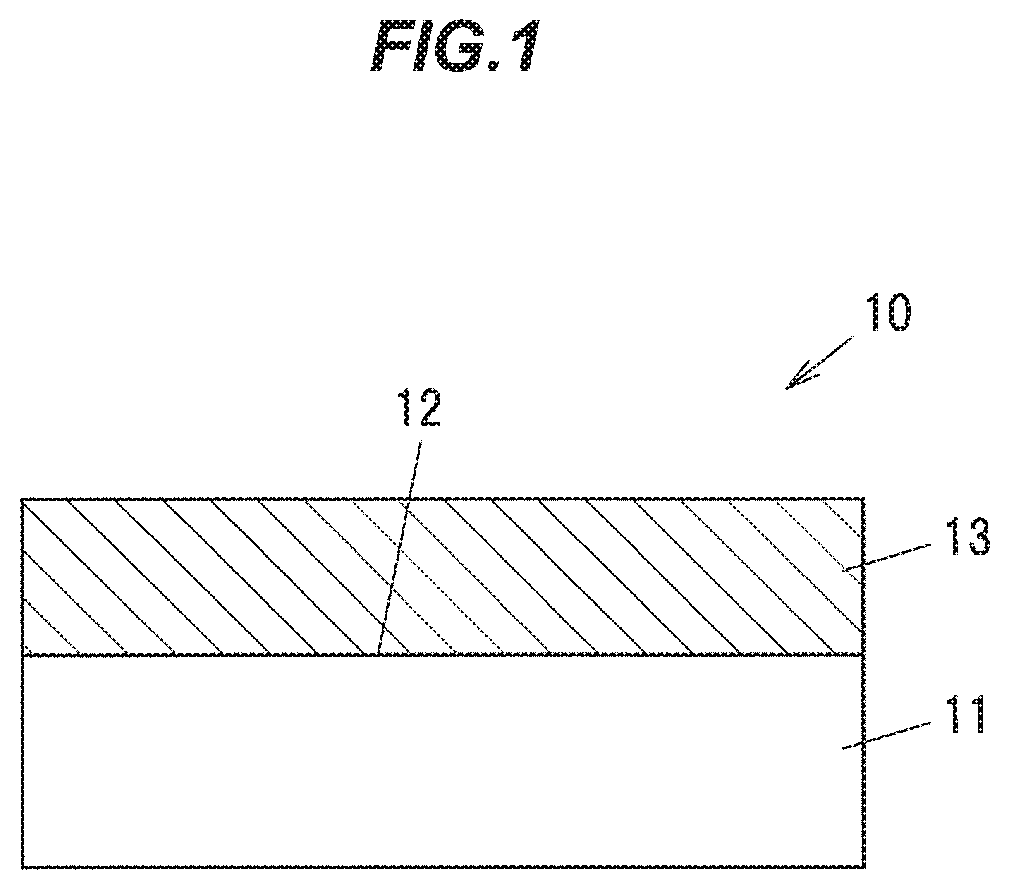
[0025] FIG. 1 is a vertical cross-sectional view showing an epitaxial wafer in the first embodiment.
[0026] FIG. 2 is a vertical cross-sectional view showing a vapor phase deposition system in the embodiment.
[0027] FIG. 3A is an optical microscope image showing a surface of an epitaxial layer.
[0028] FIG. 3B is an optical microscope image showing a surface of an epitaxial layer.
[0029] FIG. 3C is an optical microscope image showing a surface of an epitaxial layer.
[0030] FIG. 3D is an optical microscope image showing a surface of an epitaxial layer.
[0031] FIG. 4A is an optical microscope image showing a surface of an epitaxial layer.
[0032] FIG. 4B is an optical microscope image showing a surface of an epitaxial layer.
[0033] FIG. 4C is an optical microscope image showing a surface of an epitaxial layer.
[0034] FIG. 4D is an optical microscope image showing a surface of an epitaxial layer.
[0035] FIG. 5A is an optical microscope image showing a surface of an epitaxial layer.
[0036] FIG. 5B is an optical microscope image showing a surface of an epitaxial layer.
[0037] FIG. 5C is an optical microscope image showing a surface of an epitaxial layer.
[0038] FIGS. 6 (a) and (b) are an optical microscope image showing a surface of an epitaxial layer and a schematic vertical cross-sectional view showing the epitaxial layer taken along a line A-A in (a), respectively.
[0039] FIG. 7A is a scanning transmission electron microscope (STEM) bright-field image showing an upper surface of an epitaxial wafer.
[0040] FIG. 7B is a scanning transmission electron microscope (STEM) bright-field image showing a vertical cross section of the epitaxial wafer.
[0041] FIG. 8A is a conceptual diagram illustrating a relation between an angle .phi., which is formed between a dislocation line and a principal plane, and a distance D.sub.2 between dislocations appeared on the principal plane.
[0042] FIG. 8B is a conceptual diagram illustrating a relation between the angle .phi., which is formed between a dislocation line and the principal plane, and the distance D.sub.2 between dislocations appeared on the principal plane.
[0043] FIG. 9 is a graph plotting data showing a relation between an angle .theta. and the calculated length L of a V-shaped groove.
[0044] FIG. 10A is a schematic diagram illustrating change in shape of the V-shaped groove when the angle .theta. is increased in the positive direction (in a rotation direction of a right-handed screw advancing in the a-axis direction of the semiconductor substrate).
[0045] FIG. 10B is a schematic diagram illustrating change in shape of the V-shaped groove when the angle .theta. is increased in the positive direction.
[0046] FIG. 10C is a schematic diagram illustrating change in shape of the V-shaped groove when the angle .theta. is increased in the positive direction.
[0047] FIG. 10D is a schematic diagram illustrating change in shape of the V-shaped groove when the angle .theta. is increased in the positive direction.
[0048] FIG. 10E is a schematic diagram illustrating change in shape of the V-shaped groove when the angle .theta. is increased in the positive direction.
[0049] FIG. 10F is a schematic diagram illustrating change in shape of the V-shaped groove when the angle .theta. is increased in the positive direction.
[0050] FIG. 11A is a schematic diagram illustrating change in shape of the V-shaped groove when the angle .theta. is increased in the negative direction (in a rotation direction of a left-handed screw advancing in the a-axis direction of the semiconductor substrate).
[0051] FIG. 11B is a schematic diagram illustrating change in shape of the V-shaped groove when the angle .theta. is increased in the negative direction.
[0052] FIG. 11C is a schematic diagram illustrating change in shape of the V-shaped groove when the angle .theta. is increased in the negative direction.
[0053] FIG. 11D is a schematic diagram illustrating change in shape of the V-shaped groove when the angle .theta. is increased in the negative direction.
[0054] FIG. 11E is a schematic diagram illustrating change in shape of the V-shaped groove when the angle .theta. is increased in the negative direction.
[0055] FIG. 11F is a schematic diagram illustrating change in shape of the V-shaped groove when the angle .theta. is increased in the negative direction.
[0056] FIG. 12A is an optical microscope image showing the pre-CMP surface of the epitaxial layer on the semiconductor substrate with the angle .theta. of 0.06.degree..
[0057] FIG. 12B is an optical microscope image showing the post-CMP surface of the epitaxial layer on the semiconductor substrate with the angle .theta. of 0.06.degree..
[0058] FIG. 13A is a graph plotting data showing a relation between an offset angle from a (001) plane in a [100] axis direction and the growth rate of .beta.-Ga.sub.2O.sub.3 layer shown in Table 3.
[0059] FIG. 13B is a graph plotting data showing a relation between an offset angle from the (001) plane in a [010] axis direction and the growth rate of the .beta.-Ga.sub.2O.sub.3 layer shown in Table 3.
[0060] FIG. 14A is a graph plotting data showing a relation between the angle .theta. and the growth rate of the epitaxial layer shown in Table 4.
[0061] FIG. 14B is an enlarged graph showing the range of 0.degree..ltoreq..theta..ltoreq.5.5.degree. in FIG. 14A.
[0062] FIG. 15 is a vertical cross-sectional view showing a lateral transistor in the second embodiment.
DESCRIPTION OF EMBODIMENT
First Embodiment
Configuration of Crystalline Layered Structure
[0063] FIG. 1 is a vertical cross-sectional view showing an epitaxial wafer 10 in the first embodiment. The epitaxial wafer 10 has a semiconductor substrate 11 and an epitaxial layer 13 formed on a principal plane 12 of the semiconductor substrate 11 by epitaxial crystal growth using the HVPE (Halide Vapor Phase Epitaxy) method.
[0064] The semiconductor substrate 11 is a substrate formed of a .beta.-Ga.sub.2O.sub.3-based single crystal. The .beta.-Ga.sub.2O.sub.3-based single crystal here means a .beta.-Ga.sub.2O.sub.3 single crystal or a crystal of which base crystal is a .beta.-Ga.sub.2O.sub.3 single crystal doped with an element such as Al or In. The composition of the .beta.-Ga.sub.2O.sub.3 single crystal doped with, e.g., Al and In is expressed by .beta.-(Ga.sub.xAl.sub.yIn.sub.(1-x-y)).sub.2O.sub.3 (0<x.ltoreq.1, 0.ltoreq.y.ltoreq.1, 0<x+y.ltoreq.1). The band gap of the .beta.-Ga.sub.2O.sub.3 single crystal is widened by adding Al and is narrowed by adding In. The semiconductor substrate 11 may also contain a conductive impurity such as Sn.
[0065] .beta.-Ga.sub.2O.sub.3-based crystals have a .beta.-gallia structure belonging to the monoclinic system and the typical lattice constants of .beta.-Ga.sub.2O.sub.3 crystal not containing impurities are a.sub.0=12.23 .ANG., b.sub.0=3.04 .ANG., c.sub.0=5.80 .ANG., .alpha.=.gamma.=90.degree. and .beta.=103.8.degree..
[0066] To form the semiconductor substrate 11, for example, a bulk crystal of a Ga.sub.2O.sub.3-based single crystal grown by a melt-growth technique such as the FZ (Floating Zone) method or the EFG (Edge Defined Film Fed Growth) method is sliced and the surface thereof is then polished.
[0067] The principal plane 12 of the semiconductor substrate 11 is a plane parallel to a [100] axis of the .beta.-Ga.sub.2O.sub.3-based single crystal which constitutes the semiconductor substrate 11. This is determined based on the finding by the present inventors that a growth rate of a .beta.-Ga.sub.2O.sub.3-based single crystal layer epitaxially grown by the HVPE method and surface morphology of the .beta.-Ga.sub.2O.sub.3-based single crystal layer can be controlled by adjusting an angle formed between the principal plane and the (100) plane of the .beta.-Ga.sub.2O.sub.3-based single crystal when a plane orientation of the principal plane of the .beta.-Ga.sub.2O.sub.3-based single crystal substrate is parallel to the [100] axis.
[0068] When the semiconductor substrate 11 has the principal plane 12 parallel to the [100] axis and is configured so that an angle formed between the principal plane 12 and a (001) plane of a .beta.-Ga.sub.2O.sub.3-based single crystal constituting the semiconductor substrate 11 (hereinafter, referred to as "angle .theta.") is not less than -30.degree. and not more than 30.degree. where an angle generated by rotation in a rotation direction of a right-handed screw advancing in the a-axis direction of the semiconductor substrate 11 is defined as a positive angle, the growth rate of the epitaxial layer 13 formed by the HVPE method can be increased. Furthermore, the growth rate of the epitaxial layer 13 formed by the HVPE method can be further increased by adjusting the angle .theta. to not less than 0.3.degree. and not more than 15.degree., or not less than -15.degree. and not more than -0.3.degree..
[0069] In addition, surface morphology of the epitaxial layer 13 formed by the HVPE method can be improved by adjusting the angle .theta. to not less than 30.degree. and not more than 90.degree., or not less than -150.degree. and not more than -90.degree. where an angle generated by rotation in a rotation direction of a right-handed screw advancing in the a-axis direction of the semiconductor substrate 11 is defined as a positive angle.
[0070] Furthermore, surface morphology of the epitaxial layer 13 can be further improved by setting the angle .theta. to a value close to 60.degree. or -120.degree.. When the semiconductor substrate 11 has, e.g., an average dislocation density of not more than 1.times.10.sup.4/cm.sup.2, the angle .theta. is set to not less than 54.3.degree. and not more than 65.7.degree., or not less than -125.7.degree. and not more than -114.3.degree.. Then, when the semiconductor substrate 11 has an average dislocation density of not more than 1.times.10.sup.3/cm.sup.2, the angle .theta. is set to not less than 41.6.degree. and not more than 78.4.degree., or not less than -138.4.degree. and not more than -101.6.degree..
[0071] The .beta.-Ga.sub.2O.sub.3-based single crystal has symmetry. Therefore, a plane coinciding with the (001) plane rotated about the [100] axis in the positive direction is equivalent to a plane coinciding with the (001) plane rotated in the negative direction. That is, the plane orientation of the principal plane 12 is equivalent regardless of whether the angle .theta. is positive or negative.
[0072] The epitaxial layer 13 is formed of a .beta.-Ga.sub.2O.sub.3-based single crystal in the same manner as the semiconductor substrate 11. The epitaxial layer 13 may also contain a conductive impurity such as Si.
[0073] Structure of the Vapor Phase Deposition System
[0074] A structure of the vapor phase deposition system used for growing the epitaxial layer 13 in the first embodiment will be described below as an example.
[0075] FIG. 2 is a vertical cross-sectional view showing the vapor phase deposition system 2 in the embodiment. The vapor phase deposition system 2 is a vapor phase deposition system using HVPE technique, and has a reaction chamber 20 having a first gas introducing port 21, a second gas introducing port 22, a third gas introducing port 23 and an exhaust port 24, and a first heating means 26 and a second heating means 27 which are placed around the reaction chamber 20 to heat predetermined regions in the reaction chamber 20.
[0076] The film growth rate when using the HVPE technique is higher than that in the PLD method, etc. In addition, in-plane distribution of film thickness is highly uniform and it is possible to grow a large-diameter film. Therefore, it is suitable for mass production of crystal.
[0077] The reaction chamber 20 has a source reaction region R1 in which a reaction container 25 containing a Ga source is placed and a gallium source gas is produced, and a crystal growth region R2 in which the semiconductor substrate 11 is placed and the epitaxial layer 13 is grown thereon. The reaction chamber 20 is formed of, e.g., quartz glass.
[0078] Here, the reaction container 25 is formed of, e.g., quartz glass and the Ga source contained in the reaction container 25 is metal gallium.
[0079] The first heating means 26 and the second heating means 27 are capable of respectively heating the source reaction region R1 and the crystal growth region R2 of the reaction chamber 20. The first heating means 26 and the second heating means 27 are, e.g., resistive heaters or radiation heaters.
[0080] The first gas introducing port 21 is a port for introducing a Cl-containing gas (Cl.sub.2 gas or HCl gas) into the source reaction region R1 of the reaction chamber 20 using an inert carrier gas (N.sub.2 gas, Ar gas or He gas).
[0081] The second gas introducing port 22 is a port for introducing an oxygen-containing gas (O.sub.2 gas or H.sub.2O gas, etc.) as an oxygen source gas and a chloride gas (e.g., silicon tetrachloride, etc.) used to add a dopant such as Si to the epitaxial layer 13, into the crystal growth region R2 of the reaction chamber 20 using an inert carrier gas (N.sub.2 gas, Ar gas or He gas).
[0082] The third gas introducing port 23 is a port for introducing an inert carrier gas (N.sub.2 gas, Ar gas or He gas) into the crystal growth region R2 of the reaction chamber 20.
[0083] Growth of the Epitaxial Layer
[0084] A process of growing the epitaxial layer 13 in the present embodiment will be described below as an example.
[0085] Firstly, the source reaction region R1 of the reaction chamber 20 is heated by the first heating means 26 and an atmosphere temperature in the source reaction region R1 is then maintained at a predetermined temperature.
[0086] Next, in the source reaction region R1, a Cl-containing gas introduced through the first gas introducing port 21 using a carrier gas is reacted with the metal gallium in the reaction container 25 at the above-mentioned atmosphere temperature, thereby producing a gallium chloride gas.
[0087] The atmosphere temperature in the source reaction region R1 here is preferably a temperature at which GaCl gas has the highest partial pressure among component gases of the gallium chloride gas produced by the reaction of the metal gallium in the reaction container 25 with the Cl-containing gas. The gallium chloride gas here contains GaCl gas, GaCl.sub.2 gas, GaCl.sub.3 gas and (GaCl.sub.3).sub.2 gas, etc.
[0088] The temperature at which a driving force for growth of Ga.sub.2O.sub.3 crystal is maintained is the highest with the GaCl gas among the gases contained in the gallium chloride gas. Growth at a high temperature is effective to obtain a high-quality Ga.sub.2O.sub.3 crystal with high purity. Therefore, for growing the epitaxial layer 13, it is preferable to produce a gallium chloride gas in which a partial pressure of GaCl gas having a high driving force for growth at a high temperature is high.
[0089] If hydrogen is contained in an atmosphere for growing the epitaxial layer 13, surface flatness and a driving force for crystal growth of the epitaxial layer 13 decrease. Therefore, it is preferable that a Cl.sub.2 gas not containing hydrogen be used as the Cl-containing gas.
[0090] In addition, to increase a partial pressure ratio of the GaCl gas in the gallium chloride gas, it is preferable that the metal gallium in the reaction container 25 be reacted with the Cl-containing gas in a state that the atmosphere temperature in the source reaction region R1 is maintained at not less than 300.degree. C. by using the first heating means 26.
[0091] Meanwhile, at the atmosphere temperature of, e.g., not less than 850.degree. C., the partial pressure ratio of the GaCl gas is predominantly high (the equilibrium partial pressure of the GaCl gas is four orders of magnitude greater than the GaCl.sub.2 gas and is eight orders of magnitude greater than the GaCl.sub.3 gas) and the gases other than GaCl gas hardly contribute to the growth of Ga.sub.2O.sub.3 crystal.
[0092] Considering the lifetime of the first heating means 26 and heat resistance of the reaction chamber 20 formed of quartz glass, etc., it is preferable that the metal gallium in the reaction container 25 be reacted with the Cl-containing gas in a state that the atmosphere temperature in the source reaction region R1 is maintained at not more than 1000.degree. C.
[0093] Next, in the crystal growth region R2, the gallium chloride gas produced in the source reaction region R1 is mixed with the oxygen-containing gas introduced through the second gas introducing port 22 and the semiconductor substrate 11 is exposed to the resulting mixed gas, thereby epitaxially growing the epitaxial layer 13 on the semiconductor substrate 11. At this time, in a furnace housing the reaction chamber 20, pressure in the crystal growth region R2 is maintained at, e.g., 1 atm.
[0094] When forming the epitaxial layer 13 containing an additive element such as Si or Al, a source gas of the additive element (e.g., a chloride gas such as silicon tetrachloride (SiCl.sub.4)) is introduced, together with the gallium chloride gas and the oxygen-containing gas, into the crystal growth region R2 through the gas introducing port 22.
[0095] If hydrogen is contained in an atmosphere for growing the epitaxial layer 13, surface flatness and a driving force for crystal growth of the epitaxial layer 13 decrease. Therefore, it is preferable that an O.sub.2 gas not containing hydrogen be used as the oxygen-containing gas.
[0096] In addition, to suppress an increase in the equilibrium partial pressure of the GaCl gas and to efficiently grow the epitaxial layer 13, the epitaxial layer 13 is preferably grown in a state that a ratio of the supplied partial pressure of the O.sub.2 gas to the supplied partial pressure of the GaCl gas in the crystal growth region R2 is not less than 0.5.
[0097] In addition, the growth temperature is preferably not less than 900.degree. C. to grow a high-quality epitaxial layer 13.
[0098] The epitaxial layer 13 contains, e.g., not more than 5.times.10.sup.16 (atoms/cm.sup.3) of Cl. This results from that the epitaxial layer 13 is formed by the HVPE method using Cl-containing gas. Generally, Cl-containing gas is not used to form a Ga.sub.2O.sub.3 single crystal film when using a method other than the HVPE method, and the Ga.sub.2O.sub.3 single crystal film does not contain Cl, or at least does not contain 1.times.10.sup.16 (atoms/cm.sup.3) or more of Cl.
[0099] Evaluation of Surface Morphology of Epitaxial Layer
[0100] A relation between the angle .theta., which is formed between the principal plane 12 and the (001) plane of the .beta.-Ga.sub.2O.sub.3 single crystal constituting the semiconductor substrate 11, and surface morphology of the epitaxial layer 13 was evaluated. The result is as follows.
[0101] FIGS. 3A to 3D, 4A to 4D and 5A to 5C are optical microscope images showing surfaces of epitaxial layers. For the angle .theta. of the semiconductor substrate 11 as an underlying for the epitaxial layer 13, the value is indicated at the top left of each image.
[0102] The epitaxial layers 13 shown in FIGS. 3A to 3D, 4A to 4D and 5A to 5C are .beta.-Ga.sub.2O.sub.3 single crystal layers grown on the semiconductor substrates 11 formed of .beta.-Ga.sub.2O.sub.3 single crystal.
[0103] FIGS. 3A to 3D, 4A to 4D and 5A to 5C show that the more the angle .theta. becomes closer to 90.degree. from 0.degree., the shorter the length of the V-shaped groove appeared on the surface of the epitaxial layer 13 and the better the surface morphology.
[0104] Now, the V-shaped groove which deteriorates surface morphology of the epitaxial layer 13 will be described using FIGS. 6 (a) and (b).
[0105] FIG. 6 (a) is an optical microscope image showing a surface of the epitaxial layer 13 and FIG. 6 (b) is a schematic vertical cross-sectional view showing the epitaxial layer 13 taken along a line A-A in FIG. 6 (a). "L" and "T" in FIG. 6 (b) respectively indicate the length of the V-shaped groove and the thickness of the epitaxial layer 13 (the depth of the V-shaped groove). The angle .theta. of the semiconductor substrate 11 shown in FIG. 6 (a) is about +0.75.degree..
[0106] It is considered that dislocations in the semiconductor substrate 11 propagate into the epitaxial layer 13 and the V-shaped grooves are thereby formed. The inventors of the present application found that a dislocation line 15 inside the semiconductor substrate 11, which is a starting point of V-shaped groove on the epitaxial layer 13, appears at a position where the [010] axis is located when rotated by about 60.degree. in a rotation direction of a left-handed screw advancing in the a-axis direction of the semiconductor substrate 11 (in a counterclockwise direction in FIG. 6 (b)).
[0107] FIGS. 7A and 7B are scanning transmission electron microscope (STEM) bright-field images respectively showing the upper surface and the vertical cross section of the epitaxial wafer 10. The angle .theta. of the semiconductor substrate 11 shown in FIGS. 7A and 7B is about -0.8.degree.. The dislocation line 15 inside the semiconductor substrate 11 can be seen in these images.
[0108] An angle formed between a straight line 14 of the bottom of the V-shaped groove and the principal plane 12 of the semiconductor substrate 11 is equal to the angle .theta. as described later. The angle .theta. in the epitaxial wafer 10 shown in FIG. 7A is as small as -0.8.degree. and, in the STEM image with high magnification in FIG. 7B, the straight line 14 of the bottom of the V-shaped groove thus appears to coincide with the principal plane 12. Meanwhile, the side surface of the V-shaped groove is substantially perpendicular to the principal plane 12 as shown in FIG. 6 (b) but can be inclined in a very thin region in the vicinity of the principal plane 12. The semiconductor substrate 11 and the epitaxial layer 13 shown in FIG. 7A are thinned for the purpose of STEM observation, and the inclined side surface of the V-shaped groove in the vicinity of the principal plane 12 is shown in FIG. 7A.
[0109] When the angle .theta. is set to 60.degree., the dislocation lines 15 inside the semiconductor substrate 11 become parallel to the principal plane 12 and dislocations do not appear on the principal plane 12. Thus, propagation of dislocations from the semiconductor substrate 11 into the epitaxial layer 13 hardly occurs. Also when the angle .theta. is -120.degree., the dislocation lines 15 become parallel to the principal plane 12 and the length L of the V-shaped groove is thus substantially zero.
[0110] Even when the dislocation lines 15 are not completely parallel to the principal plane 12, distances between dislocations appeared on the principal plane 12 (appeared at intersections of the principal plane 12 and the dislocation lines 15) increase as closer to parallel.
[0111] FIGS. 8A and 8B are conceptual diagrams illustrating a relation between an angle .phi., which is formed between the dislocation line 15 and the principal plane 12, and a distance D.sub.2 between dislocations appeared on the principal plane 12. These conceptual diagrams are given on the assumption that the dislocation lines 15 are aligned at regular intervals.
[0112] When a distance between the dislocation lines 15 is defined as D.sub.1, the distance D.sub.2 between dislocations appeared on the principal plane 12 is equal to D.sub.1/sin .phi.. Therefore, when the angle .phi. is changed on the assumption that the distance D.sub.1 is always the same, the dislocation lines 15 become perpendicular to the principal plane 12 at .phi.=90.degree. (when the angle .theta. is 150.degree. or -30.degree.), and the distance D.sub.2 becomes equal to the distance D.sub.1 and is the smallest. Then, with the angle (9 of closer to 0.degree. (the angle .theta. of about 60.degree. or -120.degree.), the dislocation lines 15 are closer to parallel to the principal plane 12 and the distance D.sub.2 increases.
[0113] When the semiconductor substrate 11 has, e.g., an average dislocation density of not more than 1.times.10.sup.4/cm.sup.2, the average distance D.sub.1 between the dislocation lines 15 is 100 .mu.m. In this case, when the absolute value of .phi. is smaller than about 5.7.degree., the distance D.sub.2 between dislocations appeared on the principal plane 12 is greater than 100 .mu.m. That is, an average number of dislocations appeared on the principal plane 12 is less than 1/mm.sup.2.
[0114] Table 1 below shows a relation between the average dislocation density of the semiconductor substrate 11 and the angle .phi. when the average number of dislocations appeared on the principal plane 12 is less than 1/mm.sup.2.
TABLE-US-00001 TABLE 1 Average dislocation density of Semiconductor substrate Distance D.sub.2 Angle .phi. 1 .times. 10.sup.5/cm.sup.2 32 .mu.m -1.8.degree. .ltoreq. .phi. .ltoreq. 1.8.degree. 1 .times. 10.sup.4/cm.sup.2 100 .mu.m -5.7.degree. .ltoreq. .phi. .ltoreq. 5.7.degree. 1 .times. 10.sup.3/cm.sup.2 316 .mu.m -18.4.degree. .ltoreq. .phi. .ltoreq. 18.4.degree. 1 .times. 10.sup.2/cm.sup.2 1000 .mu.m .phi. .noteq. 90.degree.
[0115] .phi. is 0.degree. when the angle .theta. is about 60.degree. or -120.degree.. Therefore, according to Table 1, when the semiconductor substrate 11 has an average dislocation density of not more than 1.times.10.sup.5/cm.sup.2, the average number of dislocations appeared on the principal plane 12 can be 1/mm.sup.2 by setting the angle .theta. to not less than 58.2.degree. and not more than 61.8.degree., or not less than -121.8.degree. and not more than -118.2.degree..
[0116] In addition, when the semiconductor substrate 11 has an average dislocation density of not more than 1.times.10.sup.4/cm.sup.2, the average number of dislocations appeared on the principal plane 12 can be 1/mm.sup.2 by setting the angle .theta. to not less than 54.3.degree. and not more than 65.7.degree., or not less than -125.7.degree. and not more than -114.3.degree..
[0117] Furthermore, when the semiconductor substrate 11 has an average dislocation density of not more than 1.times.10.sup.3/cm.sup.2, the average number of dislocations appeared on the principal plane 12 can be 1/mm.sup.2 by setting the angle .theta. to not less than 41.6.degree. and not more than 78.4.degree., or not less than -138.4.degree. and not more than -101.6.degree..
[0118] Furthermore, when the semiconductor substrate 11 has an average dislocation density of not more than 1.times.10.sup.2/cm.sup.2, the average number of dislocations appeared on the principal plane 12 can be 1/mm.sup.2 by setting the angle .theta. to a value other than -30.degree. and 150.degree..
[0119] Meanwhile, the straight line 14 of the bottom of the V-shaped groove is parallel to the [010] axis of the .beta.-Ga.sub.2O.sub.3 single crystal constituting the semiconductor substrate 11. Since the cross section shown in FIG. 6 (b) is parallel to the b-axis of the .beta.-Ga.sub.2O.sub.3-based single crystal constituting the semiconductor substrate 11, the (001) plane of the semiconductor substrate 11 seen in this cross section coincides with the [010] axis. Thus, the angle .theta. formed between the principal plane 12 of the semiconductor substrate 11 and the [010] axis is equal to an angle formed between the principal plane 12 and the (001) plane (an angle formed between the straight line 14 of the bottom of the V-shaped groove and the principal plane 12) as shown in FIG. 6 (b). Therefore, according to the calculation, the length L of the V-shaped groove becomes shorter as the angle .theta. becomes closer to 90.degree..
[0120] FIG. 9 is a graph plotting data showing a relation between the length L of the V-shaped groove and the angle .theta. where an angle generated by rotation in a rotation direction of a right-handed screw advancing in the a-axis direction of the semiconductor substrate 11 is defined as a positive angle. The length L of the V-shaped groove indicated on the vertical axis in FIG. 9 is the calculated value obtained from the equation L=T/tan .theta. when the thickness T of the epitaxial layer 13 is 10 .mu.m.
[0121] Based on the curved line shown in FIG. 9, the length L of the V-shaped groove sharply decreases as .theta. becomes further from 0.degree., the curvature becomes substantially zero at around 30.degree., and after that, the length L of the V-shaped groove decreases gradually. Thus, to reduce the length L of the V-shaped groove, the angle .theta. is preferably not less than 30.degree. and not more than 90.degree., and not less than -150.degree. and not more than -90.degree. equivalent thereto.
[0122] Table 2 below shows a relation between the angle .theta., where an angle generated by rotation in a rotation direction of a right-handed screw advancing in the a-axis direction of the semiconductor substrate 11 is defined as a positive angle, and the measured values and the calculated values of the length L of the V-shaped groove.
TABLE-US-00002 TABLE 2 Length L [.mu.m] Angle .theta. [.degree.] Thickness T [.mu.m] Measured value Calculated value 0.06 2.7 500 2500 0.33 4.5 350 780 1.41 5.8 200 230 5 4.6 65 53 10 4.1 30 23 15 4.7 20 18 30 2.6 5.0 4.5 45 1.5 .apprxeq.0 1.5 60 1.3 .apprxeq.0 0.8 75 2.0 .apprxeq.0 0.5 90 1.0 .apprxeq.0 0
[0123] Among the measured values of the length L of the V-shaped groove shown in Table 2, the value at the angle .theta. of 60.degree. is substantially zero. This is because the dislocation lines 15 become parallel to the principal plane 12 and dislocations do not appear on the principal plane 12 and do not propagate into the epitaxial layer 13 as described above. The calculated values do not become zero since the calculation is performed on the assumption that dislocations propagate into the epitaxial layer 13.
[0124] Meanwhile, the measured values of the length L of the V-shaped groove at the angle .theta. of 45.degree. and 75.degree. are smaller than the calculated values and are substantially zero. This is because when the length L of the V-shaped groove is smaller than the thickness T of the epitaxial layer 13, the V-shaped groove is filled with the growing crystal in the process of growth and becomes shallow, and the length L becomes too short to measure by an optical microscope. When the length L is not more than about 0.5 .mu.m, it is difficult to find by an optical microscope. Also when the angle .theta. is -135.degree. and -105.degree., the length L of the V-shaped groove is too short to measure by an optical microscope and the measured values are substantially zero.
[0125] The measured value of the length L of the V-shaped groove is substantially zero also when the angle .theta. is 90.degree.. It is considered that this is because the [010] axis of the semiconductor substrate 11 is perpendicular to the principal plane 12 and the straight line 14 of the bottom of the V-shaped groove is thus perpendicular to the principal plane 12. Also when the angle .theta. is -90.degree., the [010] axis of the semiconductor substrate 11 is perpendicular to the principal plane 12 and the measured value of the length L of the V-shaped groove is substantially zero.
[0126] As such, by setting the angle .theta. to not less than 45.degree. and not more than 90.degree. or not less than -135.degree. and not more than -90.degree., it is possible to reduce the length L of the V-shaped groove down to the unmeasurable level by an optical microscope.
[0127] In addition, according to Table 2, the measured values of the length L of the V-shaped groove are smaller than the calculated values when the angle .theta. is small (.theta.=0.06 and 0.33). This is because the V-shaped groove is filled with the growing crystal in the process of growth of the epitaxial layer 13 and becomes shallow.
[0128] Based on the measured value of L, the depth of the V-shaped groove (the length from the surface of the epitaxial layer 13 to the lowest portion of the V-shaped groove) at .theta.=0.06 and 0.33 was calculated and the obtained values were respectively 0.52 .mu.m and 2.01 .mu.m which are smaller than the thickness of the epitaxial layer 13 shown in Table 2. This shows that the V-shaped groove was filled in the process of crystal growth when .theta.=0.06 and 0.33.
[0129] FIGS. 10A to 10F are schematic diagrams illustrating change in shape of the V-shaped groove when the angle .theta. is increased in the positive direction (in a rotation direction of a right-handed screw advancing in the a-axis direction of the semiconductor substrate 11).
[0130] FIGS. 11A to 11F are schematic diagrams illustrating change in shape of the V-shaped groove when the angle .theta. is increased in the negative direction (in a rotation direction of a left-handed screw advancing in the a-axis direction of the semiconductor substrate 11).
[0131] FIGS. 10A and 11A show the states in which the V-shaped groove is shallow and the lowest portion thereof is distant from the principal plane 12 of the semiconductor substrate 11. The states at the angle .theta. of more than 0.degree. and not more than 0.33.degree. and at the angle .theta. of less than 0.degree. and not less than -0.33.degree. described above correspond to the states shown in FIGS. 10A and 11A. Thus, it is possible to remove the V-shaped groove by performing a polishing process such as CMP (Chemical Mechanical Polishing) on the surface of the epitaxial layer 13. On the other hand, when the lowest portion of the V-shaped groove reaches the principal plane 12 of the semiconductor substrate 11, it is not possible to remove the V-shaped groove while leaving a portion of the epitaxial layer 13.
[0132] At .theta.=0.degree., the straight line 14 of the bottom of the V-shaped groove is parallel to the principal plane 12 and the length L of the V-shaped groove thus is very large (theoretically, infinity). Also in this case, the V-shaped groove is filled with the growing crystal in the process of growth of the epitaxial layer 13 and becomes shallow.
[0133] In addition, when the length L of the V-shaped groove is smaller than the thickness T of the epitaxial layer 13, the V-shaped groove is filled with the growing crystal in the process of growth and becomes shallow, as described above. In other words, when the angle .theta. is more than 45.degree. and not more than 90.degree. and when the angle .theta. is less than -45.degree. and not less than -90.degree., the V-shaped groove becomes shallow. Thus, the V-shaped grooves shown in FIGS. 10D, 10F and 11D are shallow by being filled with the growing crystal and the lowest portions thereof are distant from the principal plane 12 of the semiconductor substrate 11.
[0134] Therefore, when the angle .theta. is not less than -0.33.degree. and not more than 0.33.degree., more than 45.degree. and not more than 90.degree., or less than -45.degree. and not less than -90.degree., it is possible to remove the V-shaped groove by polishing the surface of the epitaxial layer 13.
[0135] FIGS. 12A and 12B are optical microscope images showing the surface of the epitaxial layer 13 on the semiconductor substrate 11 with the angle .theta. of 0.06.degree., wherein FIG. 12A is an image before CMP and FIG. 12B is an image after CMP. FIGS. 12A and 12B show that the V-shaped groove was removed while leaving a portion of the epitaxial layer 13.
[0136] Similar evaluation results are obtained also when the semiconductor substrate 11 and the epitaxial layer 13 are respectively formed of .beta.-Ga.sub.2O.sub.3-based single crystals other than the .beta.-Ga.sub.2O.sub.3 single crystal.
[0137] Evaluation of Growth Rate of Epitaxial Layer
[0138] Table 3 below shows a relation between offset angles of the principal plane of a .beta.-Ga.sub.2O.sub.3 substrate from the (001) plane in the [100] axis direction and the [010] axis direction and the growth rate of a .beta.-Ga.sub.2O.sub.3 layer formed on the .beta.-Ga.sub.2O.sub.3 substrate by the HVPE method.
TABLE-US-00003 TABLE 3 Offset angle [.degree.] [100] axis direction [010] axis direction Growth rate [.mu.m/h] -0.04 +0.78 6.0 +1.00 +0.50 4.3 -3.85 +0.33 4.5 -1.20 +0.06 2.7 -0.02 -0.05 3.35 +0.85 -0.44 4.5 +1.16 -1.41 5.8
[0139] Table 3 shows that the growth rate of the .beta.-Ga.sub.2O.sub.3 layer is, e.g., 6.0 .mu.m/h when grown on the .beta.-Ga.sub.2O.sub.3 substrate of which principal plane is inclined by -0.04.degree. in the [100] axis direction and 0.78.degree. in the [010] axis direction from the (001) plane.
[0140] FIG. 13A is a graph plotting data showing a relation between an offset angle from the (001) plane in the [100] axis direction and the growth rate of the .beta.-Ga.sub.2O.sub.3 layer shown in Table 3. FIG. 8B is a graph plotting data showing a relation between an offset angle from the (001) plane in the [010] axis direction and the growth rate of the .beta.-Ga.sub.2O.sub.3 layer shown in Table 3.
[0141] As shown in FIG. 13A, no regularity is found in the relation between the growth rate and the offset angle from the (001) plane in the [100] axis direction, and clear dependence of the growth rate on the offset angle in the [100] axis direction is not identified.
[0142] On the other hand, as shown in FIG. 13B, in the relation between the growth rate and the offset angle from the (001) plane in the [010] axis direction, the growth rate is the lowest at the offset angle of around 0.degree. and increases as the offset angle becomes further from 00.degree..
[0143] Table 4 below shows a relation between the angle .theta. of the semiconductor substrate 11 formed of a .beta.-Ga.sub.2O.sub.3 single crystal, i.e., the offset angle from the (001) plane in the [010] axis direction, and the growth rate of the epitaxial layer 13 formed of a .beta.-Ga.sub.2O.sub.3 single crystal.
TABLE-US-00004 TABLE 4 Angle .theta. [.degree.] Growth rate [.mu.m/h] 0.05 3.35 0.06 2.7 0.33 4.5 0.44 4.5 0.5 4.3 0.78 6.0 1.41 5.8 5 4.6 10 4.06 15 4.67 30 2.55 45 1.48 60 1.34 75 1.0 90 1.0
[0144] FIG. 14A is a graph plotting data showing a relation between the angle .theta. and the growth rate of the epitaxial layer 13 shown in Table 4. FIG. 14B is an enlarged graph showing the range of 0.degree..ltoreq..theta..ltoreq.5.5.degree. in FIG. 14A.
[0145] As shown in FIGS. 14A and 14B, the growth rate of the epitaxial layer 13 is relatively high (not less than 2.5 .mu.m/h) with the angle .theta. of not less than 0.degree. and not more than 30.degree., and is particularly high (not less than 4.0 .mu.m/h) with the angle .theta. of not less than 0.3.degree. and not more than 15.degree.. Due the symmetry of the .beta.-Ga.sub.2O.sub.3-based single crystal constituting the semiconductor substrate 11, the relation between the growth rate of the epitaxial layer 13 and the absolute value of the negative angle .theta. is the same as the relation between the growth rate of the epitaxial layer 13 and the absolute value of the positive angle .theta.. For this reason, it can be said that the growth rate of the epitaxial layer 13 is relatively high with the angle .theta. of not less than -30.degree. and not more than 30.degree., and is particularly high with the angle .theta. of not less than 0.3.degree. and not more than 15.degree., or not less than -15.degree. and not more than -0.3.degree..
[0146] For the relation between the angle .theta. and the growth rate of the epitaxial layer 13, similar results are obtained also when the semiconductor substrate 11 and the epitaxial layer 13 are respectively formed of .beta.-Ga.sub.2O.sub.3-based single crystals other than the .beta.-Ga.sub.2O.sub.3 single crystal.
Second Embodiment
[0147] The second embodiment is an embodiment of a semiconductor element including the epitaxial wafer 10 in the first embodiment. A lateral transistor having a MESFET (Metal Semiconductor Field Effect Transistor) structure will be described below as an example of such a semiconductor element.
[0148] Configuration of Semiconductor Element
[0149] FIG. 15 is a vertical cross-sectional view showing a lateral transistor 40 in the second embodiment. The lateral transistor 40 includes the epitaxial layer 13 formed on the semiconductor substrate 11, and a gate electrode 41, a source electrode 42 and a drain electrode 43 which are provided on the epitaxial layer 13. The gate electrode 41 is arranged between the source electrode 42 and the drain electrode 43.
[0150] The source electrode 42 and the drain electrode 43 are in contact with an upper surface of the epitaxial layer 13 (a surface opposite to the surface in contact with the semiconductor substrate 11) and form ohmic junctions. Meanwhile, the gate electrode 41 is in contact with the upper surface of the epitaxial layer 13 and forms a Schottky junction, and a depletion layer is thereby formed in the epitaxial layer 13 under the gate electrode 41. The lateral transistor 40 functions as either a normally-off transistor or a normally-on transistor depending on the thickness of this depletion region.
[0151] The semiconductor substrate 11 is formed of a .beta.-Ga.sub.2O.sub.3-based crystal containing a p-type dopant such as Mg, Be, Zn or Fe, and has high electrical resistance.
[0152] The epitaxial layer 13 contains an n-type dopant such as Si or Sn. The n-type dopant concentration is higher around the contact portion with the source electrode 42 and the drain electrode 43 than in other portions. The thickness of the epitaxial layer 13 is, e.g., 0.1 to 1 .mu.m.
[0153] The gate electrode 41, the source electrode 42 and the drain electrode 43 are formed of, e.g., a metal such as Au, Al, Ti, Sn, Ge, In, Ni, Co, Pt, W, Mo, Cr, Cu and Pb, an alloy containing two or more of such metals, a conductive compound such as ITO, or a conductive polymer. The conductive polymer to be used is, e.g., a polythiophene derivative (PEDOT: poly(3,4)-ethylenedioxythiophene) doped with polystyrene sulfonate (PSS) or a polypyrrole derivative doped with TCNA, etc. In addition, the gate electrode 41 may have a two-layer structure composed of two different metals, e.g., Al/Ti, Au/Ni or Au/Co.
[0154] In the lateral transistor 40, the thickness of the depletion layer in the epitaxial layer 13 under the gate electrode 41 is changed by controlling bias voltage applied to the gate electrode 41, thereby controlling a drain current.
[0155] The lateral transistor 40 described above is an example of the semiconductor element including the epitaxial wafer 10 in the first embodiment, and the epitaxial wafer 10 can be used to manufacture various other semiconductor elements.
[0156] It is possible to manufacture, e.g., MISFET (Metal Insulator Semiconductor Field Effect Transistor) and HEMT (High Electron Mobility Transistor) in which the epitaxial layer 13 is used as a channel layer, and Schottky diode in which the semiconductor substrate 11 and the epitaxial layer 13 are respectively connected to an ohmic electrode and a Schottky electrode. Type and concentration of dopants contained in the semiconductor substrate 11 and the epitaxial layer 13 are appropriately determined according to the type of semiconductor element to be manufactured.
[0157] A region of the epitaxial layer 13 without any V-shaped grooves and a crystal layer formed on such region are used to manufacture semiconductor elements including the lateral transistor 40. That is, the better the surface morphology of the epitaxial layer 13, the more the semiconductor elements obtained from one wafer.
Effects of the Embodiments
[0158] In the embodiment described above, the growth rate of the epitaxial layer 13 formed by the HVPE method can be further increased by adjusting the angle .theta. of the semiconductor substrate 11 to not less than 0.degree. and not more than 30.degree., more preferably not less than 0.3.degree. and not more than 15.degree.. As a result, it is possible to efficiently form the epitaxial layer 13. In addition, by growing the epitaxial layer 13 at a high growth rate, it is possible to reduce diffusion of impurities from the semiconductor substrate 11 and thus possible to increase quality.
[0159] In addition, surface morphology of the epitaxial layer 13 formed by the HVPE method can be further improved by adjusting the angle .theta. of the semiconductor substrate 11 to not less than 30.degree. and not more than 90.degree.. This increases an area of the epitaxial layer 13 which can be used to form semiconductor elements and it is thus possible to improve the production yield of the semiconductor element.
[0160] Although the embodiments of the invention have been described, the invention is not intended to be limited to the embodiments, and the various kinds of modifications can be implemented without departing from the gist of the invention.
[0161] In addition, the invention according to claims is not to be limited to the embodiments described above. Further, it should be noted that all combinations of the features described in the embodiments are not necessary to solve the problem of the invention.
INDUSTRIAL APPLICABILITY
[0162] Provided are a semiconductor substrate comprising a .beta.-Ga.sub.2O.sub.3-based single crystal on which an epitaxial layer comprising a .beta.-Ga.sub.2O.sub.3-based single crystal can be grown by the HVPE method at a high growth rate or on which an epitaxial layer comprising a .beta.-Ga.sub.2O.sub.3-based single crystal having good surface morphology can be grown; an epitaxial wafer having the semiconductor substrate and an epitaxial layer; and a method for producing the epitaxial wafer.
REFERENCE SIGNS LIST
[0163] 10 EPITAXIAL WAFER [0164] 11 SEMICONDUCTOR SUBSTRATE [0165] 12 PRINCIPAL PLANE [0166] 13 EPITAXIAL LAYER
* * * * *
D00000
D00001
D00002
D00003
D00004
D00005
D00006
D00007
D00008
D00009
D00010
D00011
D00012

D00013

D00014

D00015

XML
uspto.report is an independent third-party trademark research tool that is not affiliated, endorsed, or sponsored by the United States Patent and Trademark Office (USPTO) or any other governmental organization. The information provided by uspto.report is based on publicly available data at the time of writing and is intended for informational purposes only.
While we strive to provide accurate and up-to-date information, we do not guarantee the accuracy, completeness, reliability, or suitability of the information displayed on this site. The use of this site is at your own risk. Any reliance you place on such information is therefore strictly at your own risk.
All official trademark data, including owner information, should be verified by visiting the official USPTO website at www.uspto.gov. This site is not intended to replace professional legal advice and should not be used as a substitute for consulting with a legal professional who is knowledgeable about trademark law.