Selective Plasma Etching Of Silicon Oxide Relative To Silicon Nitride By Gas Pulsing
Zhang; Du ; et al.
U.S. patent application number 16/739889 was filed with the patent office on 2020-07-23 for selective plasma etching of silicon oxide relative to silicon nitride by gas pulsing. The applicant listed for this patent is Tokyo Electron Limited. Invention is credited to Yu-Hao Tsai, Mingmei Wang, Du Zhang.
| Application Number | 20200234968 16/739889 |
| Document ID | / |
| Family ID | 71610134 |
| Filed Date | 2020-07-23 |


| United States Patent Application | 20200234968 |
| Kind Code | A1 |
| Zhang; Du ; et al. | July 23, 2020 |
SELECTIVE PLASMA ETCHING OF SILICON OXIDE RELATIVE TO SILICON NITRIDE BY GAS PULSING
Abstract
A method for selective plasma etching of silicon oxide relative to silicon nitride. The method includes a) providing a substrate containing a silicon oxide film and a silicon nitride film, b) exposing the substrate to a plasma-excited treatment gas containing 1) H.sub.2 and 2) HF, F.sub.2, or both HF and F.sub.2, to form a silicon oxide surface layer with reduced oxygen content on the silicon oxide film and form an ammonium salt layer on the silicon nitride film, c) exposing the substrate to a plasma-excited halogen-containing gas that reacts with and removes the silicon oxide surface layer from the silicon oxide film, and d) repeating steps b) and c) at least once to further selectively etch the silicon oxide film relative to the ammonium salt layer on the silicon nitride film. The ammonium salt layer may be removed when the desired etching has been achieved.
| Inventors: | Zhang; Du; (Albany, NY) ; Tsai; Yu-Hao; (Albany, NY) ; Wang; Mingmei; (Albany, NY) | ||||||||||
| Applicant: |
|
||||||||||
|---|---|---|---|---|---|---|---|---|---|---|---|
| Family ID: | 71610134 | ||||||||||
| Appl. No.: | 16/739889 | ||||||||||
| Filed: | January 10, 2020 |
Related U.S. Patent Documents
| Application Number | Filing Date | Patent Number | ||
|---|---|---|---|---|
| 62793893 | Jan 18, 2019 | |||
| 62926754 | Oct 28, 2019 | |||
| Current U.S. Class: | 1/1 |
| Current CPC Class: | H01L 21/31116 20130101; H01L 21/32137 20130101; H01L 21/3065 20130101 |
| International Class: | H01L 21/311 20060101 H01L021/311; H01L 21/3065 20060101 H01L021/3065; H01L 21/3213 20060101 H01L021/3213 |
Claims
1. A plasma processing method, comprising: a) providing a substrate containing a silicon oxide film and a silicon nitride film; b) exposing the substrate to a plasma-excited treatment gas containing 1) H.sub.2 and 2) HF, F.sub.2, or both HF and F.sub.2, to form a silicon oxide surface layer with reduced oxygen content on the silicon oxide film and form an ammonium salt layer on the silicon nitride film; c) exposing the substrate to a plasma-excited halogen-containing gas that reacts with and removes the silicon oxide surface layer from the silicon oxide film; and d) repeating steps b) and c) at least once to further selectively etch the silicon oxide film relative to the ammonium salt layer on the silicon nitride film.
2. The method of claim 1, wherein the plasma-excited treatment gas contains or consists of 1) H.sub.2 and HF; 2) H.sub.2, HF, and a noble gas; 3) H.sub.2 and F.sub.2; 4) H.sub.2, F.sub.2, and a noble gas; 5) H.sub.2, HF, and F.sub.2; or 6) H.sub.2, HF, F.sub.2, and a noble gas.
3. The method of claim 1, wherein the silicon oxide film includes SiO.sub.2 and the silicon oxide surface layer includes SiO.sub.x, where x<2.
4. The method of claim 1, wherein the silicon nitride film includes Si.sub.3N.sub.4.
5. The method of claim 1, wherein the ammonium salt layer includes NH.sub.4F, (NH.sub.4).sub.2SiF.sub.6, or a combination thereof.
6. The method of claim 1, wherein the plasma-excited halogen-containing gas includes CF.sub.4, CHF.sub.3, CH.sub.2F.sub.2, CH.sub.3F, NF.sub.3, SF.sub.6, Cl.sub.2, CCl.sub.4, SiCl.sub.4, SiH.sub.2Cl.sub.2, CHCl.sub.3, HBr, Br.sub.2, or SiBr.sub.4, or a combination thereof.
7. The method of claim 1, wherein the plasma-excited halogen-containing gas includes a fluorocarbon gas, a hydrofluorocarbon gas, or a combination thereof.
8. The method of claim 1, wherein the plasma-excited halogen-containing gas contains CF.sub.4, CHF.sub.3, CH.sub.2F.sub.2, or CH.sub.3F, or a combination thereof.
9. The method of claim 1, further comprising; following step d), e) removing the ammonium salt layer from the silicon nitride film.
10. The method of claim 9, further comprising f) repeating steps b)-e) at least once to further selectively etch the silicon oxide film.
11. A plasma processing method, comprising: a) providing a substrate containing a silicon oxide film and a silicon nitride film; b) exposing the substrate to a plasma-excited H.sub.2-containing gas to form a silicon oxide surface layer with reduced oxygen content on the silicon oxide film and form a hydrogenated silicon nitride surface layer on the silicon nitride film; c) exposing the substrate to a plasma-excited halogen-containing gas that reacts with and removes the silicon oxide surface layer from the silicon oxide film and forms an ammonium salt layer from the hydrogenated silicon nitride surface layer; and d) repeating steps b) and c) at least once to further selectively etch the silicon oxide film relative to the ammonium salt layer on the silicon nitride film.
12. The method of claim 11, wherein the plasma-excited H.sub.2-containing gas consists of H.sub.2, or H.sub.2 and a noble gas.
13. The method of claim 11, wherein the silicon oxide film includes SiO.sub.2 and the silicon oxide surface layer includes SiO.sub.x, where x<2.
14. The method of claim 11, wherein the silicon nitride film includes Si.sub.3N.sub.4.
15. The method of claim 11, wherein the ammonium salt layer includes NH.sub.4X, (NH.sub.4).sub.2SiX.sub.6, or a combination thereof, where X is a halogen.
16. The method of claim 11, wherein the plasma-excited halogen-containing gas includes CF.sub.4, CHF.sub.3, CH.sub.2F.sub.2, CH.sub.3F, NF.sub.3, SF.sub.6, Cl.sub.2, CCl.sub.4, SiCl.sub.4, SiH.sub.2Cl.sub.2, CHCl.sub.3, HBr, Br.sub.2, or SiBr.sub.4, or a combination thereof.
17. The method of claim 11, wherein the plasma-excited halogen-containing gas includes a fluorocarbon gas, a hydrofluorocarbon gas, or a combination thereof.
18. The method of claim 11, wherein the plasma-excited halogen-containing gas contains CF.sub.4, CHF.sub.3, CH.sub.2F.sub.2, CH.sub.3F, or a combination thereof.
19. The method of claim 11, further comprising; following step d), e) removing the ammonium salt layer from the silicon nitride film.
20. The method of claim 19, further comprising f) repeating steps b)-e) at least once to further selectively etch the silicon oxide film.
Description
CROSS-REFERENCE TO RELATED APPLICATIONS
[0001] This application is related to and claims priority to U.S. Provisional Patent Application Ser. No. 62/793,893 filed on Jan. 18, 2019, the entire contents of which are herein incorporated by reference. This application is related to and claims priority to U.S. Provisional Patent Application Ser. No. 62/926,754 filed on Oct. 28, 2019, the entire contents of which are herein incorporated by reference.
FIELD OF INVENTION
[0002] The present invention relates to the field of semiconductor manufacturing and semiconductor devices, and more particularly, to a method of selective plasma etching of silicon oxide relative to silicon nitride in semiconductor manufacturing.
BACKGROUND OF THE INVENTION
[0003] Next generation semiconductor technology development poses a huge challenge as dry etch removal of one material selective to other materials is needed, for example in the etching of <5 nm contacts. In silicon oxide or silicon nitride etching by plasmas containing fluorocarbon (FC) or hydrofluorocarbon (HFC) gases, a fluorinated carbon layer is typically formed on the film surface. The thickness, density, and atomic compositions of such a carbon layer depend on the kinetic energies and fluxes of incident ions and charge-neutral species from the plasma and strongly affect the etch rate of the material beneath it.
SUMMARY OF THE INVENTION
[0004] A method of selective plasma etching of silicon oxide relative to silicon nitride in semiconductor manufacturing is disclosed in several embodiments.
[0005] According to one embodiment, the method includes a) providing a substrate containing a silicon oxide film and a silicon nitride film, b) exposing the substrate to a plasma-excited treatment gas containing 1) H.sub.2 and 2) HF, F.sub.2, or both HF and F.sub.2, to form a silicon oxide surface layer with reduced oxygen content on the silicon oxide film and form an ammonium salt layer on the silicon nitride film, c) exposing the substrate to a plasma-excited halogen-containing gas that reacts with and removes the silicon oxide surface layer from the silicon oxide film, and d) repeating steps b) and c) at least once to further selectively etch the silicon oxide film relative to the ammonium salt layer on the silicon nitride film. According to one embodiment, the method further includes removing the ammonium salt layer from the silicon nitride film when the desired etching of the silicon oxide film has been achieved.
[0006] According to another embodiment, the method includes a) providing a substrate containing a silicon oxide film and a silicon nitride film, b) exposing the substrate to a plasma-excited H.sub.2-containing gas to form a silicon oxide surface layer with reduced oxygen content on the silicon oxide film and form a hydrogenated silicon nitride surface layer on the silicon nitride film, c) exposing the substrate to a plasma-excited halogen-containing gas that reacts with and removes the silicon oxide surface layer from the silicon oxide film and forms an ammonium salt layer from the hydrogenated silicon nitride surface layer, and d) repeating steps b) and c) at least once to further selectively etch the silicon oxide film relative to the ammonium salt layer on the silicon nitride film. According to one embodiment, the method further includes removing the ammonium salt layer from the silicon nitride film when the desired etching of the silicon oxide film has been achieved.
DETAILED DESCRIPTION OF THE DRAWINGS
[0007] In the accompanying drawings:
[0008] FIGS. 1A-1G schematically show through cross-sectional views a method of selective plasma etching of a silicon oxide film relative to a silicon nitride film by gas pulsing according to an embodiment of the invention; and
[0009] FIGS. 2A-2G schematically show through cross-sectional views a method of selective plasma etching of a silicon oxide film relative to a silicon nitride film by gas pulsing according to another embodiment of the invention.
DETAILED DESCRIPTION OF SEVERAL EMBODIMENTS
[0010] A method of selective plasma etching of silicon oxide relative to silicon nitride by gas pulsing is described. Embodiments of the invention utilize diverging surface chemical reactions of silicon oxide and silicon nitride films by sequential plasma exposures of A) 1) H.sub.2 and 2) HF, F.sub.2, or both HF and F.sub.2, and B) a halogen-containing gas at substrate temperature and gas pressure conditions that achieve selective etching of the silicon oxide film relative to the silicon nitride film. The method includes repeated cycles of a two-step process that is described with respect to surface reactions on the silicon oxide and silicon nitride films, leading to selective etching of the silicon oxide film. According to one embodiment, in the first step A), a plasma exposure of 1) H.sub.2 and 2) HF, F.sub.2, or both HF and F.sub.2, is performed that results in chemical surface reduction of the silicon oxide film and formation of an ammonium salt layer on the silicon nitride film. Thereafter, in the second step B), a halogen-containing plasma treatment is performed that results in formation and desorption of volatile byproducts from the reduced silicon oxide film. At the end of each cycle of the two-step process, a portion of the silicon oxide film is removed, a silicon oxide film surface is restored, while the layer of an ammonium salt that is formed on silicon nitride film serves as a blocking layer.
[0011] According to one embodiment, in the first step, a H.sub.2 plasma treatment is performed that results in chemical surface reduction of the silicon oxide film and chemical surface hydrogenation of the silicon nitride film. Thereafter, in the second step, a halogen-containing plasma treatment is performed that results in formation and desorption of volatile byproducts from the reduced silicon oxide film and halogen incorporation into the surface hydrogenated silicon nitride film to form an ammonium salt layer. At the end of each cycle of the two-step process, a portion of the silicon oxide film is removed, a silicon oxide film surface is restored, while the layer of an ammonium salt that is formed on silicon nitride film that serves as an etch blocking layer.
[0012] The inventive selective plasma etching process of silicon oxide relative to silicon nitride described in embodiments of the invention fundamentally differs from conventional silicon oxide or silicon nitride etching process by plasmas containing fluorocarbon (FC) or hydrofluorocarbon (HFC) gases. This allows for selective passivation on the Si.sub.3N.sub.4 film relative to the SiO.sub.2 film. In the inventive process, an ammonium salt layer latter is formed in a bottom-up manner with nitrogen (N) provided from the hydrogenated Si.sub.3N.sub.4 surface layer or the Si.sub.3N.sub.4 film, whereas in the conventional etching process, a fluorinated carbon layer is formed in a top-down manner on the substrate surface during the etching process.
[0013] The method of selective plasma etching of SiO.sub.2 films relative to Si.sub.3N.sub.4 films may be performed in conventional commercial plasma processing systems, including Inductively Coupled Plasma (ICP) systems, Capacitively Coupled Plasma (CCP) systems, remote plasma systems that generate plasma excited species upstream from the substrate, electron cyclotron resonance (ECR) systems, and other systems.
[0014] FIGS. 1A-1G schematically show through cross-sectional views a method of selective plasma etching of a SiO.sub.2 film relative to a Si.sub.3N.sub.4 film by gas pulsing according to an embodiment of the invention. The method combines selective ammonium salt formation on the Si.sub.3N.sub.4 film and selective chemical reduction of the SiO.sub.2 film to provide highly controllable and selective SiO.sub.2/Si.sub.3N.sub.4 etching.
[0015] FIG. 1A schematically shows a substrate 1 containing a SiO.sub.2 film 100 and a Si.sub.3N.sub.4 film 120. In the example shown in FIG. 1A, the SiO.sub.2 film 100 and the Si.sub.3N.sub.4 film 120 are in the same horizontal plane, but embodiments of the invention may also be applied to films that are not in the same horizontal plane but are offset vertically. Si.sub.3N.sub.4 is the most thermodynamically stable of the silicon nitrides and hence the most commercially important of the silicon nitrides. However, embodiments of the invention may be applied to other silicon nitrides that contain Si and N as the major constituents, where the silicon nitrides can have a wide range of Si and N compositions. Similarly, SiO.sub.2 is the most thermodynamically stable of the silicon oxides and hence the most commercially important of the silicon oxides. However, embodiments of the invention may be applied to other silicon oxides that contain Si and O as the major constituents, where the silicon oxides can have a wide range of Si and O compositions.
[0016] The method includes exposing the substrate 1 to a plasma-excited treatment gas 101 that is hydrogen-fluorine-based as is schematically shown in FIG. 1B. The treatment gas can contain or consist of 1) H.sub.2 and HF; 2) H.sub.2, HF, and a noble gas, 3) H.sub.2 and F.sub.2, 4) H.sub.2, F.sub.2, and a noble gas, 5) H.sub.2, HF, and F.sub.2, or 6) H.sub.2, HF, F.sub.2, and a noble gas (e.g., argon (Ar) or helium (He)). Hydrogen ions (H.sup.+) and hydrogen radicals (H.) in the plasma-excited treatment gas 101 react with the SiO.sub.2 film 100 and facilitate oxygen (O) removal via O--H bond formation and subsequent formation and desorption of volatile H.sub.2O from the SiO.sub.2 film 100. The plasma exposure forms a SiO.sub.x (x<2) surface layer 102 on the SiO.sub.2 film 100, where the SiO.sub.x (x<2) surface layer 102 has low O-content and high Si-content relative to the SiO.sub.2 film 100. The hydrogen ions (H.sup.-), hydrogen radicals (H.), and plasma excited HF, F.sub.2, or both HF and F.sub.2, react with the Si.sub.3N.sub.4 film 120 to form an ammonium salt layer 122 containing NH.sub.4F and (NH.sub.4).sub.2SiF.sub.6. It is contemplated that the exposure to the plasma excited treatment gas forms Lewis bases such as --NH-- and --NH.sub.2 surface species, as well as NH.sub.3 molecules. These Lewis bases subsequently react with acidic HF species to form the ammonium salt layer 122. FIG. 1C schematically shows the substrate 1 following the exposure to the plasma-excited treatment gas 101.
[0017] Thereafter, the method further includes exposing the substrate 1 to a halogen-containing plasma. In one embodiment, the halogen-containing plasma can include a plasma-excited halogen-containing gas 103, where the plasma-excited halogen-containing gas 103 reacts with and removes the SiO.sub.x surface layer 102 from the SiO.sub.2 film 100 but the ammonium salt layer 122 protects the underlying Si.sub.3N.sub.4 film 120 from etching. Possible volatile reaction products include SiX.sub.4 and CO.sub.aX.sub.b. This is schematically shown in FIGS. 1D and 1E. According to one embodiment, the halogen-containing gas can include a fluorine-containing gas (e.g. CF.sub.4, CHF.sub.3, CH.sub.2F.sub.2, CH.sub.3F, NF.sub.3, or SF.sub.6, or a combination thereof), a chlorine-containing gas (e.g. Cl.sub.2, CCl.sub.4, SiCl.sub.4, SiH.sub.2Cl.sub.2, or CHCl.sub.3, or a combination thereof), a bromine-containing gas (e.g. HBr, Br.sub.2, or SiBr.sub.4, or a combination thereof), or a combination thereof. The halogen-containing gas can further include an additive gas (e.g. O.sub.2, N.sub.2, or CO.sub.2, or a combination thereof). In some examples, the halogen-containing gas can include HBr and O.sub.2, Cl.sub.2 and O.sub.2, or HBr, Cl.sub.2 and O.sub.2. According to another embodiment, the halogen-containing gas can include a fluoro-carbon-based gas that includes a fluorocarbon gas, a hydrofluorocarbon gas, or a combination thereof. The fluorocarbon-based gas may further contain a non-polymerizing gas (e.g., Ar, He, SF.sub.6, or a combination thereof). For example, the fluorocarbon gas can contain or consist of CF.sub.4, and the hydrofluorocarbon gas can contain or consist of CHF.sub.3, CH.sub.2F.sub.2, CH.sub.3F, or a combination thereof. The sequential and alternating steps of exposing the substrate 1 to the plasma-excited treatment gas 101 and exposing the substrate 1 to the plasma-excited halogen-containing gas 103 may be repeated at least once to further selectively etch the SiO.sub.2 film 100 relative to the ammonium salt layer 122 on the Si.sub.3N.sub.4 film 120. The resulting substrate 1 is shown in FIG. 1F. The steps of pulsing the plasma-excited treatment gas 101 and the plasma-excited halogen-containing gas 103 may be interrupted by gas purging steps that remove the plasma species and any gaseous reaction byproducts from the plasma chamber.
[0018] According to one embodiment, the method further includes removing the ammonium salt layer 122 from the Si.sub.3N.sub.4 film 120 (e.g., by wet cleaning, heating, or IR irradiation) when the desired etching of the SiO.sub.2 film 100 has been achieved. The resulting substrate 1 is shown in FIG. 1G. According to one embodiment, the method further includes, following the removal of the ammonium salt layer 122 from the Si.sub.3N.sub.4 film 120, repeating the sequential and alternating steps of exposing the substrate 1 to the plasma-excited treatment gas 101 and exposing the substrate 1 to the plasma-excited halogen-containing gas 103 at least once to further selectively etch the SiO.sub.2 film 100, and thereafter, removing the ammonium salt layer 122 from the Si.sub.3N.sub.4 film 120.
[0019] Halogen species generated in the plasma-excited halogen-containing gas 103 react with the SiO surface layer 102 to form volatile SiX.sub.4 species (where X is a halogen), and CO.sub.aX.sub.b species when using a carbon-containing gas (e.g., CCl.sub.4 or CHCl.sub.3), that desorb from the substrate 1 and thereby etch the SiO surface layer 102 and restore a SiO.sub.2 surface. In contrast, the ammonium salt layer 122 protects the underlying Si.sub.3N.sub.4 film 120 from etching by the plasma-excited halogen-containing gas 103. Thus, the ammonium salt layer 122 functions as an etch stop layer (blocking layer) that hinders or prevents further modification/etching of the underlying Si.sub.3N.sub.4 film 120 when the steps of exposing the substrate 1 to the plasma-excited treatment gas 101, and exposing the substrate 1 to a plasma-excited halogen-containing gas 103, are repeated at least once to further selectively etch the SiO.sub.2 film 100 relative to the Si.sub.3N.sub.4 film 120.
[0020] The selective SiO.sub.2/Si.sub.3N.sub.4 etching process may be performed at substrate temperatures and gas pressures that optimize 0 removal from the SiO.sub.2 film 100 by the plasma-excited treatment gas 101, optimize the ammonium salt formation on the Si.sub.3N.sub.4 film 120, and optimize the etching of the SiO surface layer 102 by the plasma-excited halogen-containing gas 103. Examples include a substrate temperature between about -100.degree. C. and about 25.degree. C., between about -100.degree. C. and about -30.degree. C., between about -100.degree. C. and about 0.degree. C., between about -30.degree. C. and about 25.degree. C., or between about 0.degree. C. and about 25.degree. C. The gas pressure in the plasma etch chamber can between about 10 mTorr and about 500 mTorr, between about 10 mTorr and 200 mTorr, or between about 20 mTorr and about 100 mTorr. Further, the use of low energy ions in the plasma that impinge on the substrate 1 provides good SiO.sub.2/Si.sub.3N.sub.4 etch selectivity, provides good control over the SiO.sub.2 etch depth per cycle, avoids or reduces excessive physical sputtering of Si.sub.3N.sub.4 film 120 and the ammonium salt layer 124, and reduces the ion implantation depth. Still further, the addition of the non-polymerizing gas may be used during the exposure to the carbon-containing gas to enhance the removal of the SiO.sub.x surface layer 102.
[0021] FIGS. 2A-2G schematically show through cross-sectional views a method of selective plasma etching of a SiO.sub.2 film relative to a Si.sub.3N.sub.4 film by gas pulsing according to another embodiment of the invention. The method combines selective ammonium salt formation on the Si.sub.3N.sub.4 film and selective chemical reduction of the SiO.sub.2 film to provide highly controllable and selective SiO.sub.2/Si.sub.3N.sub.4 etching.
[0022] FIG. 2A schematically shows a substrate 2 containing a SiO.sub.2 film 200 and a Si.sub.3N.sub.4 film 220. In the example shown in FIG. 2A, the SiO.sub.2 film 200 and the Si.sub.3N.sub.4 film 220 are in the same horizontal plane, but embodiments of the invention may also be applied to films that are not in the same horizontal plane but are offset vertically.
[0023] The method includes treating the substrate 2 with a H.sub.2-based plasma that can include plasma-excited H.sub.2-containing gas 201 as is schematically shown in FIG. 2B. The H.sub.2-containing gas can, for example, consist of H.sub.2, or H.sub.2 and a noble gas (e.g., argon (Ar) or helium (He)).
[0024] Hydrogen ions (H.sup.+) and hydrogen radicals (H.) in the plasma-excited H.sub.2-containing gas 201 react with the SiO.sub.2 film 200 and facilitate oxygen (O) removal via O--H bond formation and subsequent formation and desorption of volatile H.sub.2O from the SiO.sub.2 film 200. The plasma exposure forms a SiO.sub.x (x<2) surface layer 202 on the SiO.sub.2 film 200, where the SiO.sub.x (x<2) surface layer 202 has low O-content and high Si-content relative to the SiO.sub.2 film 200. In contrast, the hydrogen ions (H.sup.+) and the hydrogen radicals (H.) react with the Si.sub.3N.sub.4 film 220 by surface hydrogenation/protonation rather than nitrogen (N) removal, thereby forming a hydrogenated Si.sub.3N.sub.4 surface layer 222 that is ammonium (NH.sub.4.sup.+)-rich. FIG. 2C schematically shows the substrate 1 following the exposure to the plasma-excited H.sub.2-containing gas 201.
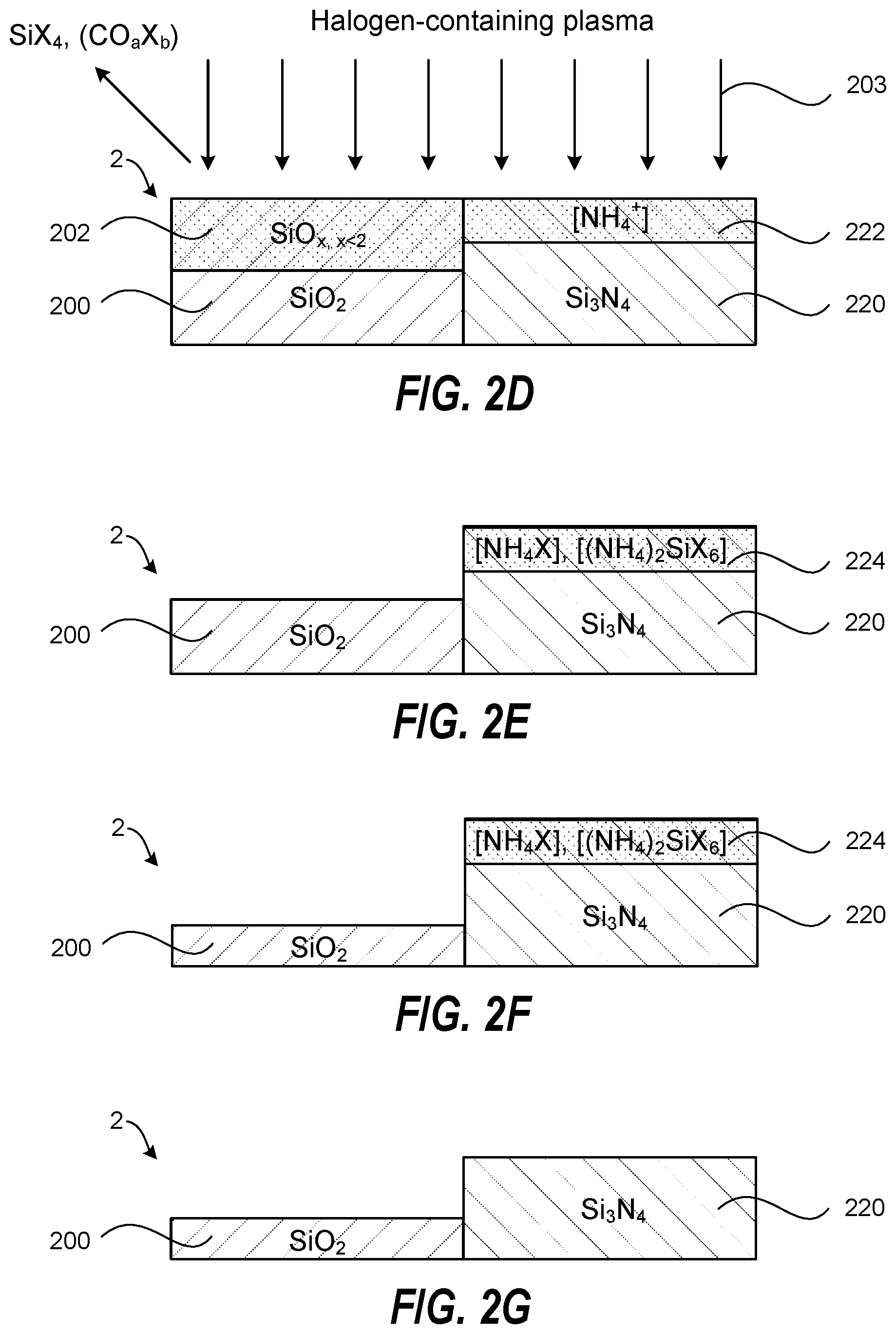
[0025] Thereafter, the method further includes exposing the substrate 2 to a plasma-excited halogen-containing gas 203, where the exposing reacts with and removes the SiO.sub.x surface layer 202 from the SiO.sub.2 film 200 and forms an ammonium salt layer 224 by reacting with the hydrogenated silicon nitride surface layer 222. This is schematically shown in FIGS. 2D and 2E. Some of the different halogen-containing gases and additive gases that may be used were described above in reference to FIG. 1D.
[0026] The sequential and alternating steps of treating the substrate 2 with the plasma-excited H.sub.2-containing gas 201 and exposing the substrate 2 to the plasma-excited halogen-containing gas 203 may be repeated at least once to further selectively etch the SiO.sub.2 film 200 relative to the ammonium salt layer 224 on the Si.sub.3N.sub.4 film 220. The resulting substrate 2 is shown in FIG. 2F. The steps of pulsing the plasma-excited H.sub.2-containing gas 201 and the plasma-excited halogen-containing gas 203 may be interrupted by gas purging steps that remove the plasma species and any gaseous reaction byproducts from the plasma chamber. According to one embodiment, the method further includes removing the ammonium salt layer 224 from the Si.sub.3N.sub.4 film 220 when the desired etching of the SiO.sub.2 film 100 has been achieved (e.g. by wet cleaning, heating, or IR irradiation). The resulting substrate 2 is shown in FIG. 2G. According to one embodiment, the method further includes, following the removing of the ammonium salt layer 224 from the Si.sub.3N.sub.4 film 220, repeating the sequential and alternating steps of exposing the substrate 2 with the plasma-excited H.sub.2-containing gas 201 and exposing the substrate 2 to the plasma-excited halogen-containing gas 203 at least once to further selectively etch the SiO.sub.2 film 200, and thereafter, removing the ammonium salt layer 224 from the Si.sub.3N.sub.4 film 120.
[0027] Halogen species generated in the plasma-excited halogen-containing gas 203 react with the SiO, surface layer 202 to form volatile SiX.sub.4 (where X is a halogen), and CO.sub.aX.sub.b species when using a carbon-containing gas, that desorb from the substrate 2 and thereby etch the SiO.sub.x surface layer 202 and restore a SiO.sub.2 surface. In contrast, the species generated in the plasma-excited halogen-containing gas 203 react with the hydrogenated Si.sub.3N.sub.4 surface layer 222 to form the ammonium salt layer 224 that functions as an etch stop layer (blocking layer) that hinders or prevents further modification/etching of the underlying Si.sub.3N.sub.4 film 220 when the steps of treating the substrate 2 with the plasma-excited H.sub.2-containing gas 201, and exposing the substrate 2 to the plasma-excited halogen-containing gas 203, are repeated at least once to further selectively etch the SiO.sub.2 film 200 relative to the Si.sub.3N.sub.4 film 220.
[0028] The selective SiO.sub.2/Si.sub.3N.sub.4 etching process may be performed at substrate temperatures and gas pressures that optimize O removal from the SiO.sub.2 film 200 by the plasma-excited H.sub.2-containing gas 201, and optimize the ammonium salt formation on the Si.sub.3N.sub.4 film 220 by the plasma-excited halogen-containing gas 203. Examples include a substrate temperature between about -100.degree. C. and about 25.degree. C., between about -100.degree. C. and about -30.degree. C., between about -100.degree. C. and about 0.degree. C., between about -30.degree. C. and about 25.degree. C., or between about 0.degree. C. and about 25.degree. C. The gas pressure in the plasma etch chamber can between about 10 mTorr and about 500 mTorr, between about 10 mTorr and 200 mTorr, or between about 20 mTorr and about 100 mTorr. Further, the use of low energy of ions in the plasma that impinge on the substrate 2 provides good SiO.sub.2/Si.sub.3N.sub.4 etch selectivity, provides good control over the SiO.sub.2 etch depth per cycle, avoids or reduces excessive physical sputtering of Si.sub.3N.sub.4 film 220 and the ammonium salt layer 224, and reduces the ion implantation depth. Still further, the addition of a non-polymerizing gas may be used during the exposure to the carbon-containing gas to enhance the removal of the SiO.sub.x surface layer 202.
[0029] A plurality of embodiments for a method of selective plasma etching of silicon oxide relative to silicon nitride in semiconductor manufacturing have been described. The foregoing description of the embodiments of the invention has been presented for the purposes of illustration and description. It is not intended to be exhaustive or to limit the invention to the precise forms disclosed. This description and the claims following include terms that are used for descriptive purposes only and are not to be construed as limiting. Persons skilled in the relevant art can appreciate that many modifications and variations are possible in light of the above teaching. Persons skilled in the art will recognize various equivalent combinations and substitutions for various components shown in the Figures. It is therefore intended that the scope of the invention be limited not by this detailed description, but rather by the claims appended hereto.
* * * * *
D00000
D00001
D00002
D00003
D00004
XML
uspto.report is an independent third-party trademark research tool that is not affiliated, endorsed, or sponsored by the United States Patent and Trademark Office (USPTO) or any other governmental organization. The information provided by uspto.report is based on publicly available data at the time of writing and is intended for informational purposes only.
While we strive to provide accurate and up-to-date information, we do not guarantee the accuracy, completeness, reliability, or suitability of the information displayed on this site. The use of this site is at your own risk. Any reliance you place on such information is therefore strictly at your own risk.
All official trademark data, including owner information, should be verified by visiting the official USPTO website at www.uspto.gov. This site is not intended to replace professional legal advice and should not be used as a substitute for consulting with a legal professional who is knowledgeable about trademark law.