Charge Trap Evaluation Method And Semiconductor Element
KAKUSHIMA; Kuniyuki ; et al.
U.S. patent application number 16/641129 was filed with the patent office on 2020-06-25 for charge trap evaluation method and semiconductor element. This patent application is currently assigned to SUMITOMO CHEMICAL COMPANY, LIMITED. The applicant listed for this patent is SUMITOMO CHEMICAL COMPANY, LIMITED. Invention is credited to Takuya HOSHII, Hiroshi IWAI, Kuniyuki KAKUSHIMA, Kazuo TSUTSUI, Hitoshi WAKABAYASHI, Taiki YAMAMOTO.
| Application Number | 20200203493 16/641129 |
| Document ID | / |
| Family ID | 65439855 |
| Filed Date | 2020-06-25 |

| United States Patent Application | 20200203493 |
| Kind Code | A1 |
| KAKUSHIMA; Kuniyuki ; et al. | June 25, 2020 |
CHARGE TRAP EVALUATION METHOD AND SEMICONDUCTOR ELEMENT
Abstract
Provided are a charge trap evaluation method and semiconductor device including, in an embodiment, a step for applying an initialization voltage that has the same sign as a threshold voltage and is greater than or equal to the threshold voltage between the source electrode 15 and drain electrode 16 of a semiconductor device 1 having an HEMT structure and the substrate 10 of the semiconductor device 1 and initializing a trap state by forcing out trapped charge from a trap level and a step for monitoring the current flowing between the source electrode 15 and drain electrode 16 after the trap state initialization and evaluating at least one from among charge trapping, current collapse, and charge release.
| Inventors: | KAKUSHIMA; Kuniyuki; (Yokohama, JP) ; HOSHII; Takuya; (Yokohama, JP) ; WAKABAYASHI; Hitoshi; (Yokohama, JP) ; TSUTSUI; Kazuo; (Yokohama, JP) ; IWAI; Hiroshi; (Yokohama, JP) ; YAMAMOTO; Taiki; (Hitachi-shi, JP) | ||||||||||
| Applicant: |
|
||||||||||
|---|---|---|---|---|---|---|---|---|---|---|---|
| Assignee: | SUMITOMO CHEMICAL COMPANY,
LIMITED Tokyo JP |
||||||||||
| Family ID: | 65439855 | ||||||||||
| Appl. No.: | 16/641129 | ||||||||||
| Filed: | August 6, 2018 | ||||||||||
| PCT Filed: | August 6, 2018 | ||||||||||
| PCT NO: | PCT/JP2018/029483 | ||||||||||
| 371 Date: | February 21, 2020 |
| Current U.S. Class: | 1/1 |
| Current CPC Class: | H01L 29/812 20130101; G01R 31/26 20130101; H01L 29/4234 20130101; G01R 31/2621 20130101; H01L 29/0847 20130101; H01L 29/778 20130101 |
| International Class: | H01L 29/423 20060101 H01L029/423; H01L 29/778 20060101 H01L029/778; H01L 29/08 20060101 H01L029/08; G01R 31/26 20060101 G01R031/26 |
Foreign Application Data
| Date | Code | Application Number |
|---|---|---|
| Aug 24, 2017 | JP | 2017-161603 |
Claims
1. A charge trap evaluation method, comprising: a step for applying an initialization voltage having the same sign as a threshold voltage and a magnitude equal to or greater than the threshold voltage between a source electrode and a drain electrode of a semiconductor device having a lateral structure and a substrate of the semiconductor device and initializing a trap state by expelling a trapped charge from a trap level; and a step for monitoring a current flowing between the source electrode and the drain electrode after the trap state initialization and evaluating at least one from among charge capture, current collapse, and charge release, wherein the threshold voltage is a voltage applied between the source and drain electrodes and the substrate, and on-off state of channel current switches when the voltage is applied between the source electrode and the drain electrode.
2. The charge trap evaluation method according to claim 1, wherein the charge capture is evaluated by evaluating the charge capture when the voltage applied between the source and drain electrodes and the substrate is changed from the initialization voltage to a stress voltage having the same sign as the threshold voltage and a magnitude equal to or less than the threshold voltage, after the trap state initialization.
3. The charge trap evaluation method according to claim 2, wherein the current collapse is evaluated by changing the voltage between the source and drain electrodes and the substrate from the stress voltage to 0V, after the evaluation of the charge capture, and calculating a ratio of a current value immediately after the voltage becomes 0V to a saturated current value after a predetermined time has elapsed.
4. The charge trap evaluation method according to claim 3, wherein the charge release is evaluated by evaluating the charge release when the voltage between the source and drain electrodes and the substrate is changed from 0V to the stress voltage after the evaluation of the current collapse.
5. The charge trap evaluation method according to claim 1, wherein the semiconductor device includes a semiconductor layer having a bandgap of 2.5 eV or more.
6. A semiconductor device with a lateral structure, comprising: a substrate; a semiconductor layer on the substrate; and a source electrode and a drain electrode which are connected to the semiconductor layer, wherein a trapped charge can be expelled from a trap level and a trap state can be initialized by applying a voltage having the same sign as a threshold voltage and a magnitude equal to or greater than the threshold voltage.
7. The semiconductor device according to claim 6, wherein the semiconductor layer has a bandgap of 2.5 eV or more.
8. A semiconductor device with a lateral structure, comprising: a substrate; a semiconductor layer on the substrate; and a source electrode and a drain electrode which are connected to the semiconductor layer, wherein in a curve showing a relationship between a voltage applied between the source and drain electrodes and a substrate and a current flowing between the source electrode and the drain electrode, a voltage in a range where hysteresis is observed is applied to the substrate as a stress voltage, a time rate of change of a value of the current when the stress voltage is released is 10% or less.
9. The charge trap evaluation method according to claim 2, wherein the semiconductor device includes a semiconductor layer having a bandgap of 2.5 eV or more.
10. The charge trap evaluation method according to claim 3, wherein the semiconductor device includes a semiconductor layer having a bandgap of 2.5 eV or more.
11. The charge trap evaluation method according to claim 4, wherein the semiconductor device includes a semiconductor layer having a bandgap of 2.5 eV or more.
Description
TECHNICAL FIELD
[0001] The present invention relates to a charge trap evaluation method and a semiconductor device.
BACKGROUND ART
[0002] As a problem to be solved for a so-called power semiconductor device, in particular, for a HEMT (High Electron Mobility Transistor), there is a phenomenon called as "current collapse" in which the on-resistance increases. When the current collapse occurs, on-loss increases, switching failure and the like may occur, which may cause deterioration of characteristics of the power semiconductor device. It is considered that the current collapse is generated by charge trapped in a trap level in a semiconductor layer or the like due to voltage stress applied to the OFF state of the HEMT. Here, "charge trap" means that not only electrons but also charges including holes are trapped. This is because hole trapping in addition to electron trapping are considered to affect the on-resistance.
[0003] As a conventional method for evaluating the current collapse, a method of applying voltage of 100 to 200V at which the current collapse can occur between two ohmic electrodes on a surface of the GaN-HEMT and a substrate, thereby evaluating a ratio of resistance values of the voltage between the two ohmic electrodes before and after the voltage application has been known (e.g., see Non-Patent Literature 1).
[0004] According to the method of Non-Patent Literature 1, since a vertical voltage is applied to the HEMT in order to generate a current collapse, the collapse due to the vertical electric field can be evaluated.
CITATION LIST
Patent Literature
[0005] Non-Patent Literature 1: YOSHIOKA Akira and 4 others, "Current Collapse Phenomena of GaN-HEMTs Caused By Vertical Electric Field on Conductive Substrates", Materials of IEICE Technical Meeting. EFM, Electronic Materials Technical Meeting, Nov. 30, 2007, EFM-07-18, pp. 15-19
SUMMARY OF INVENTION
Technical Problem
[0006] However, the method of Non-Patent Literature 1 has a problem that measurement reproducibility is low when a semiconductor device using a wide bandgap semiconductor having a deep trap level is used as a sample. For example, even if the samples are exactly the same, the measured values vary every time the measurement is performed.
[0007] It is an object of the present invention to provide a charge trap evaluation method for electrons and holes, which ensures the measurement reproducibility even for a semiconductor device using a wide bandgap semiconductor having a deep trap level, and makes it possible to evaluate the current collapse with high reproducibility, and a semiconductor device that can be evaluated with good reproducibility by the same method.
Solution to Problem
[0008] One embodiment of the present invention provides the following charge trap evaluation methods [1] to [5] and the semiconductor devices [6] to [8] to achieve the above object.
[0009] [1] A charge trap evaluation method, comprising: [0010] a step for applying an initialization voltage having the same sign as a threshold voltage and a magnitude equal to or greater than the threshold voltage between a source electrode and a drain electrode of a semiconductor device having a lateral structure and a substrate of the semiconductor device and initializing a trap state by expelling a trapped charge from a trap level; and [0011] a step for monitoring a current flowing between the source electrode and the drain electrode after the trap state initialization and evaluating at least one from among charge capture, current collapse, and charge release, [0012] wherein the threshold voltage is a voltage applied between the source and drain electrodes and the substrate, and on-off state of channel current switches when the voltage is applied between the source electrode and the drain electrode.
[0013] [2] The charge trap evaluation method according to [1], wherein the charge capture is evaluated by evaluating the charge capture when the voltage applied between the source and drain electrodes and the substrate is changed from the initialization voltage to a stress voltage having the same sign as the threshold voltage and a magnitude equal to or less than the threshold voltage, after the trap state initialization.
[0014] [3] The charge trap evaluation method according to [2], wherein the current collapse is evaluated by changing the voltage between the source and drain electrodes and the substrate from the stress voltage to 0V, after the evaluation of the charge capture, and calculating a ratio of a current value immediately after the voltage becomes 0V to a saturated current value after a predetermined time has elapsed.
[0015] [4] The charge trap evaluation method according to [3], wherein the charge release is evaluated by evaluating the charge release when the voltage between the source and drain electrodes and the substrate is changed from 0V to the stress voltage after the evaluation of the current collapse.
[0016] [5] The charge trap evaluation method according to any one of [1] to [4], wherein the semiconductor device includes a semiconductor layer having a bandgap of 2.5 eV or more.
[0017] [6] A semiconductor device with a lateral structure, comprising: [0018] a substrate; [0019] a semiconductor layer on the substrate; and [0020] a source electrode and a drain electrode which are connected to the semiconductor layer,
[0021] wherein a trapped charge can be expelled from a trap level and a trap state can be initialized by applying a voltage having the same sign as a threshold voltage and a magnitude equal to or greater than the threshold voltage.
[0022] [7] The semiconductor device according to [6], wherein the semiconductor layer has a bandgap of 2.5 eV or more.
[0023] [8] A semiconductor device with a lateral structure, comprising: [0024] a substrate; [0025] a semiconductor layer on the substrate; and [0026] a source electrode and a drain electrode which are connected to the semiconductor layer, [0027] wherein in a curve showing a relationship between a voltage applied between the source and drain electrodes and a substrate and a current flowing between the source electrode and the drain electrode, a voltage in a range where hysteresis is observed is applied to the substrate as a stress voltage, a time rate of change of a value of the current when the stress voltage is released is 10% or less.
Advantageous Effects of Invention
[0028] According to the present invention, it is possible to provide a charge trap evaluation method capable of ensuring measurement reproducibility even for a semiconductor device using a wide bandgap semiconductor having a deep trap level and performing a current collapse evaluation with good reproducibility, and a semiconductor device which can be evaluated with good reproducibility by the same method.
BRIEF DESCRIPTION OF DRAWINGS
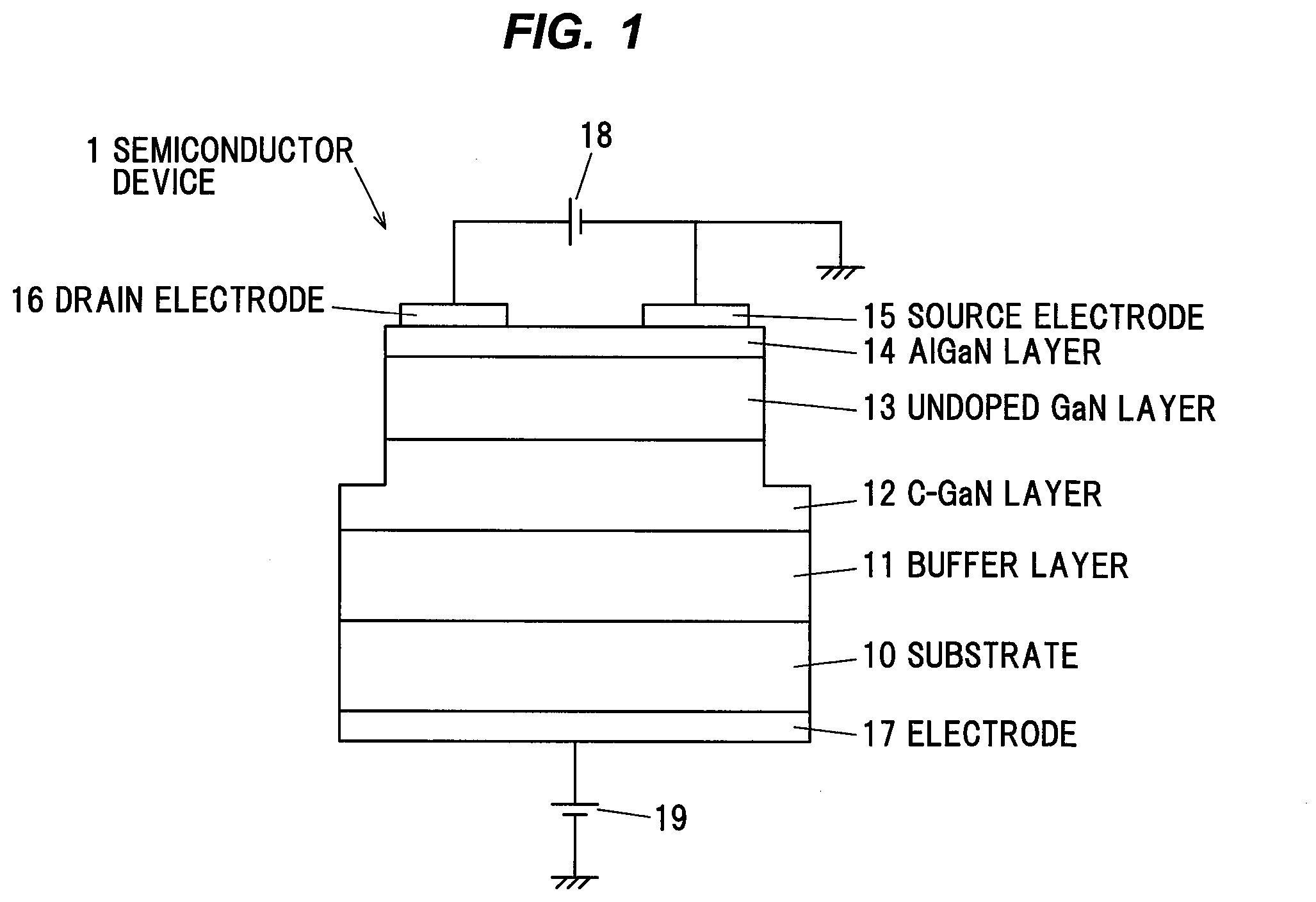
[0029] FIG. 1 is a vertical sectional view of an example of a semiconductor device having a structure suitable for evaluation by the charge trap evaluation method according to the present embodiment.
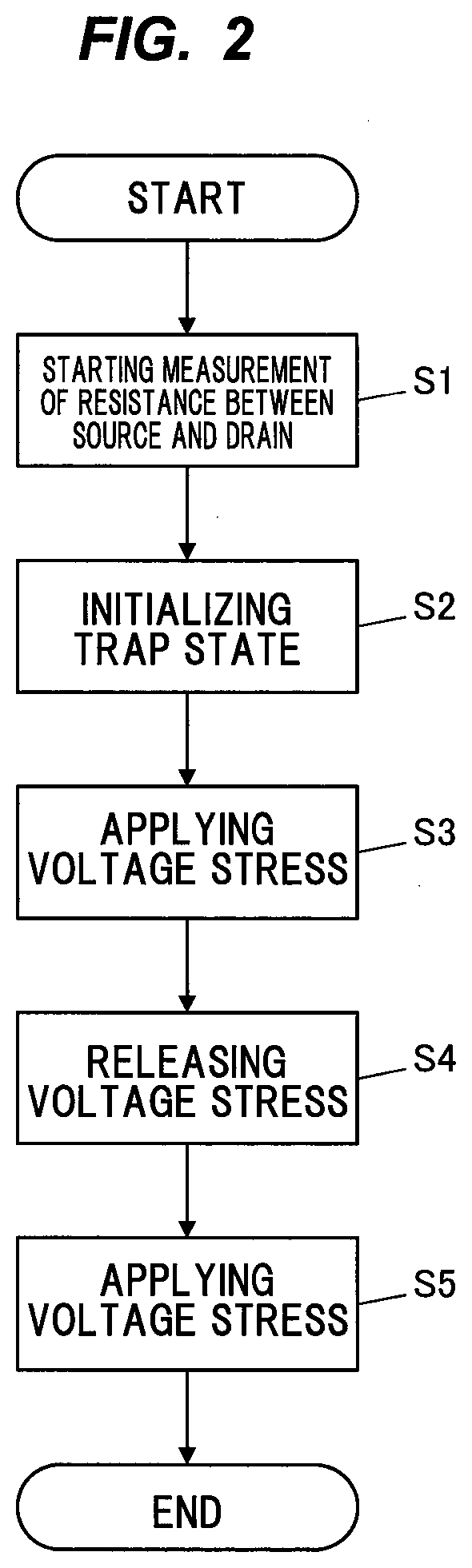
[0030] FIG. 2 is a flowchart showing a flow of the charge trap evaluation method according to the present embodiment.
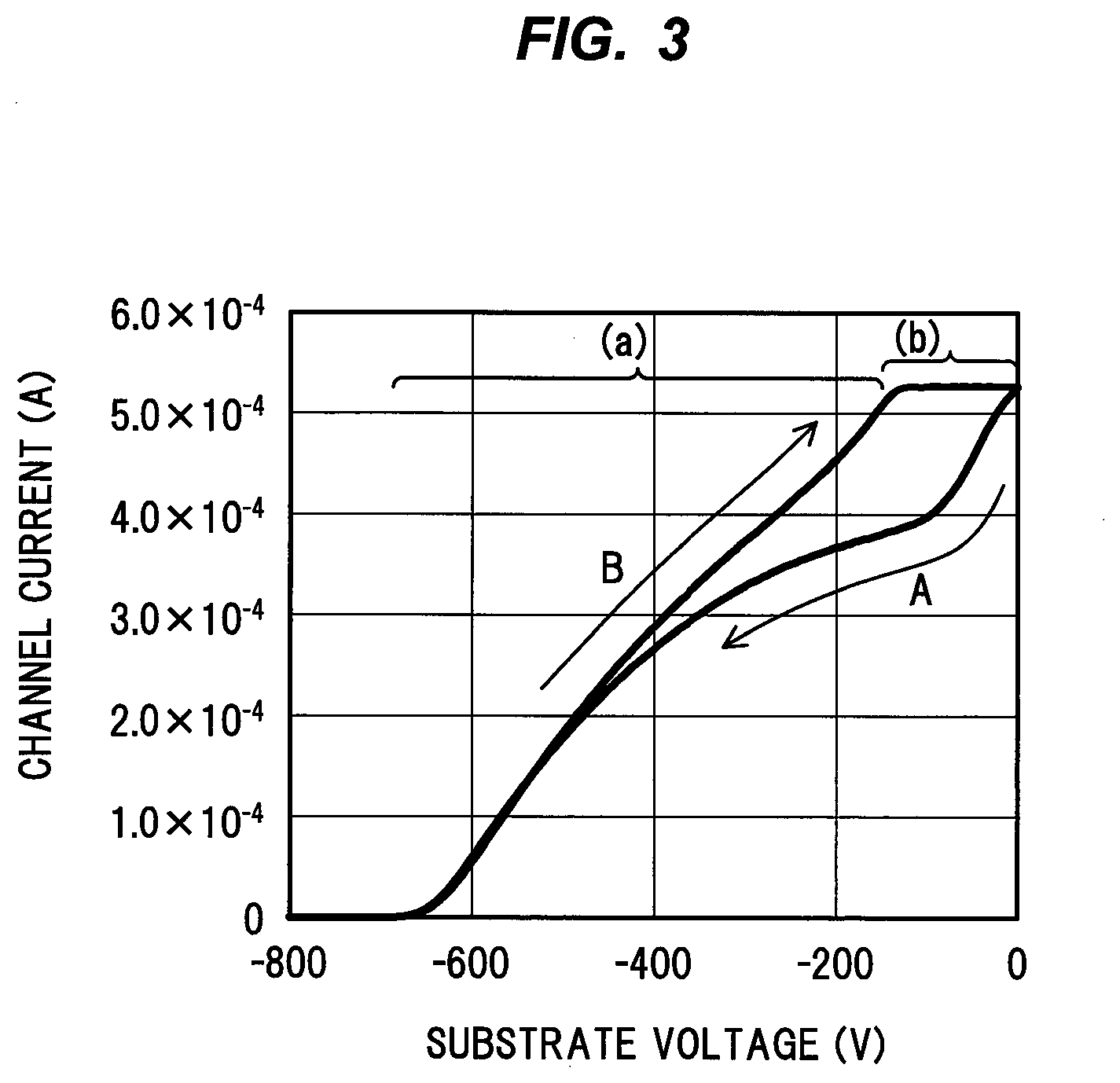
[0031] FIG. 3 is a graph showing a relationship between a voltage applied between source and drain electrodes and a substrate and a channel current flowing between the source electrode and the drain electrode in the example of the present invention.
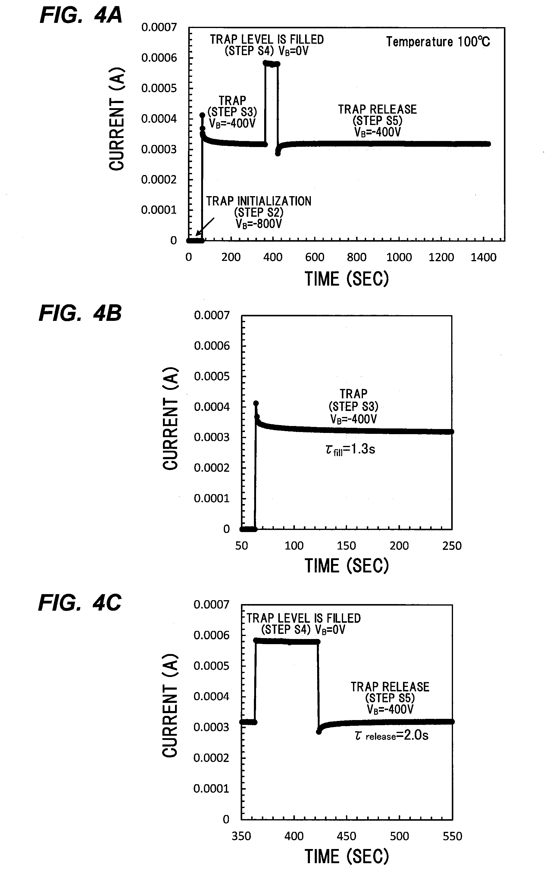
[0032] FIG. 4A is a graph showing a channel current flowing between the source electrode and the drain electrode during steps S2 to S5 in the embodiment of the present invention.
[0033] FIG. 4B is a graph in which a part of FIG. 4A is enlarged.
[0034] FIG. 4C is a graph in which a part of FIG. 4A is enlarged.
DESCRIPTION OF EMBODIMENT
[0035] The inventors have contemplated that there is some disturbance factor in the initial state of measurement with respect to the problem of low measurement reproducibility in the current collapse evaluation of a semiconductor device using a wide bandgap semiconductor represented by HEMT. As a result of intensive studies, the inventors assumed that the wide bandgap semiconductor has a deep trap level, so that it would be difficult to reach a complete thermal equilibrium state, and that the charge trap state during measurement would vary. Therefore, a method for initializing the charge trap state before the measurement was examined.
[0036] Conventionally, there have been known methods of initializing a trap state by irradiating light or heating on a sample of a semiconductor device. Methods of initializing the trap state after measuring the trap state have been also known. However, with these methods, it is difficult to initialize the trap state of semiconductor devices including wide bandgap semiconductors before measuring the trap state. In addition, since a light irradiation or heating step and an equipment therefor are required separately from the step of applying a voltage, the number of steps and the number of devices increase.
[0037] Therefore, the inventors achieved the solution for the above problem by applying a voltage having the same sign as a threshold voltage and a magnitude equal to or greater than the threshold voltage in a pre-process of trap state measurement by voltage application, and expelled trapped charges from the trap level to change the trap state, thereby initializing the trap state (ideally, releasing all trapped charges from the trap level). Further, according to the semiconductor device which is most suitable for evaluation using the trap charge evaluation method including the above-described steps, quality variation can be reduced, so that the yield rate of non-defective products is increased, and finally the production yield can be improved.
[0038] Still further, the same effect as the above-described semiconductor device can be obtained by providing a semiconductor device in which a time rate of change of the value of the current flowing between the source electrode and the drain electrode is set in a specific range, when the voltage is applied between the source and drain electrodes and the substrate using the above-described trap charge evaluation method.
(Semiconductor Device 1)
[0039] FIG. 1 is a vertical sectional view of a semiconductor device 1 which is an example of a semiconductor device having a structure suitable for evaluation by the charge trap evaluation method according to the present embodiment.
[0040] The semiconductor device 1 includes a substrate 10 made of a semiconductor such as Si, a buffer layer 11 made of a plurality of semiconductor layers such as AIN and AlGaN laminated on the substrate 10 in order, a first nitride semiconductor layer 12 made of a nitride semiconductor such as GaN doped with impurities, a second nitride semiconductor layer 13 to which impurities are not added, a third nitride semiconductor layer 14 made of AlGaN or the like, and a source electrode 15 and a drain electrode 16 that are connected to a surface (opposite surface with respect to the second nitride semiconductor layer 13) of the third nitride semiconductor layer 14, and an electrode 17 connected to a back surface of the substrate 10 (opposite surface with respect to the buffer layer 11).
[0041] The first nitride semiconductor layer 12 is a layer made of a GaN film to which, e.g., C (carbon) is added as an impurity, and the second nitride semiconductor layer 12b is a layer made of, e.g., (an undoped) GaN film to which no impurity is added. The third nitride semiconductor layer 14 is a layer made of, e.g., AlGaN.
[0042] The source electrode 15 and the drain electrode 16 are, e.g., linear electrodes having a width W.sub.mes of about several tens .mu.m to several hundred .mu.m, e.g., and an interval L.sub.gap between the source electrode 15 and the drain electrode 16 is about several tens .mu.m to several hundred .mu.m. The electrode 17 may be formed on, for example, the entire back surface of the substrate 10. As an example, each of the source electrode 15 and the drain electrode 16 has a laminated structure composed of a plurality of metals such as Ti/Al/Ni/ Au, and the electrode 17 has a laminated structure composed of a plurality of metals such as Ni/Au.
[0043] The voltage can be applied between the source electrode 15 and the drain electrode 16 by a DC power supply 18. Thereby, a channel current is flown between the source electrode 15 and the drain electrode 16 through two-dimensional electron gas in vicinity of an interface between the second nitride semiconductor layer 13 and the third nitride semiconductor layer 14, in the second nitride semiconductor layer 13.
[0044] The channel current I.sub.ch is a current flowing between the source electrode 15 and the drain electrode 16 when a constant (e.g., 1V) voltage is applied between the source electrode 15 and the drain electrode 16 by the DC power supply 18.
[0045] The voltage can be applied between the source and drain electrodes 15, 16 and the substrate 10 by a DC power supply 19.
[0046] A substrate voltage V.sub.B is a voltage applied between the source and drain electrodes 15, 16 and the substrate 10 by the DC power supply 19, and it has a positive value when the source electrode 15 and the drain electrode 16 have a low potential and the substrate 10 has a high potential. Takes a positive value.
[0047] In this embodiment, the semiconductor device 1 has a HEMT structure, but when used as a sample, a gate electrode, between a source electrode and a drain electrode, which is unnecessary for charge trap evaluation is omitted from a normal three-terminal HEMT, and an electrode is further provided on the back surface of the substrate. Note that the semiconductor device 1 may have a gate electrode.
(Charge Trap Evaluation Method)
[0048] FIG. 2 is a flowchart showing a flow of the charge trap evaluation method according to the present embodiment. Hereinafter, the charge trap evaluation method will be described with reference to the flowchart of FIG. 2. In the present embodiment, the following steps are performed under a constant temperature condition (e.g., 100.degree. C.) in order to reduce disturbance factors of the measured value.
[0049] First, a constant voltage is applied between the source electrode 15 and the drain electrode 16 by the DC power supply 18, and the current I.sub.ch flowing between the source electrode 15 and the drain electrode 16 is monitored (Step S1).
[0050] Next, a voltage having the same sign as the threshold voltage V.sub.th and a magnitude equal to or higher than the threshold voltage V.sub.th (referred to as "an initialization voltage V.sub.i,") is applied between the source and drain electrodes 15, 16 and the substrate 10 by the DC power supply 19. Then, the trapped state is initialized by expelling the charges trapped in the trap levels of the buffer layer 11, the first nitride semiconductor layer 12, and the second nitride semiconductor layer 13 (Step S2).
[0051] The value of the initialization voltage V.sub.i; will be described later, but the voltage application time can be arbitrarily set based on the overall structure, the threshold voltage, the composition of each layer, and the like of the device. As an example, the initialization voltage may be set to be applied for one minute but is not limited thereto. For example, the voltage may be applied in a range from 1 second to 60 minutes.
[0052] The threshold voltage V.sub.th is a voltage applied between the source and drain electrodes 15, 16 and the substrate 10, and is a voltage at which the channel current I.sub.ch between the source electrode 15 and the drain electrode 16 is switched on and off when the voltage is applied between the source electrode 15 and the drain electrode 16.
[0053] Next, a voltage (stress voltage V.sub.s) having the same sign as the threshold voltage V.sub.th and a magnitude less than or equal to the threshold voltage Vth is applied between the source and drain electrodes 15, 16 and the substrate 10 by the DC power supply 19, so that a voltage stress is applied (step S3).
[0054] In the semiconductor device 1, when the threshold voltage V.sub.th, is, e.g., -700V, the stress voltage V.sub.s can be set to -700V or more, typically -600 to -100V. However, the stress voltage V.sub.s is not limited to a negative voltage but can be a positive voltage. Further, the numerical range of stress voltage V.sub.s can be set based on a voltage region where hysteresis is observed in a substrate voltage VB-channel current I.sub.ch curve described later.
[0055] By applying the stress voltage V.sub.s, charges are trapped so as to reach a quasi-equilibrium state in a state where the stress voltage V.sub.s is applied. At this time, the charge trap can be monitored from the change in the current flowing between the source electrode 15 and the drain electrode 16.
[0056] After the trap state has been initialized, in order to prevent the charges from being trapped again before moving to the step S2, it is preferable that the steps S1 and S2 are continuously performed that is, the substrate voltage V.sub.B is switched from the initialization voltage V.sub.i directly to the stress voltage V.sub.s.
[0057] Next, the substrate voltage V.sub.B is set to 0V, and the charge trap is evaluated by calculating the ratio between the current value immediately after the substrate voltage V.sub.B becomes 0V and the saturated current value after a certain period of time (Step S4).
[0058] Next, the stress voltage V.sub.s is applied between the source and drain electrodes 15, 16 and the substrate 10 by the DC power supply 19 again, that is, the voltage stress is applied with using the substrate voltage V.sub.B as the stress voltage V.sub.s (Step S5).
[0059] At this time, the trapped charge is released when the voltage V.sub.B is set to 0V, so that the charge release can be monitored from the change in the current I.sub.ch flowing between the source electrode 15 and the drain electrode 16.
[0060] According to the present embodiment, the charge trap when the stress voltage is applied is evaluated in the step S3, and the charge trap in the state where the stress voltage is not applied (voltage V.sub.B is 0V) after the stress voltage has been applied is evaluated in the step S4 (That is, the current collapse is evaluated), then the charge release at the time of applying the stress voltage in the step S5 can be evaluated.
[0061] Note that it is assumed that in the conventional charge trap evaluation method that does not include the trap state initialization step (step S2) of the present embodiment, the measurement reproducibility in the current collapse evaluation is low and the accuracy and stability of the evaluation of charge release are poor because the dispersion of the initial state of measurement is large. This is presumably because the wide bandgap semiconductor has a deep trap level, so that it is difficult to reach a perfect thermal equilibrium state, and the state of the charge trap at the time of measurement varies from device to device.
[0062] Therefore, it can be said that the semiconductor device 1 suitable for the charge trap evaluation method of the present embodiment is a semiconductor device having a horizontal structure, which includes a substrate 10, semiconductor layers 11 to 14 on the substrate 10, and a source electrode 15 and a drain electrode 16 which are connected to the semiconductor layers 11 to 14, in which trapped charges can be expelled from a trap level by applying a stress voltage V.sub.s having the same sign as a threshold voltage V.sub.th and a magnitude equal to or higher than the threshold voltage V.sub.th between the source electrode 15 and the drain electrode 16 and the substrate 10, thereby the trap state can be initialized.
[0063] Alternatively, the semiconductor device 1 may be a semiconductor device which includes a substrate 10, semiconductor layers 11 to 14 on the substrate 10, and a source electrode 15 and a drain electrode 16 which are connected to the semiconductor layers 11 to 14, in which in a curve showing a relationship between a substrate voltage V.sub.B applied between the source and drain electrode, 15, 16 and a substrate electrode 19 and a current I.sub.ch flowing between the source electrode 15 and the drain electrode 16, a voltage in a range where hysteresis is observed is applied to the substrate 10 as the stress voltage V.sub.s, a time rate of change of the value of the current I.sub.ch when the stress voltage V.sub.s is released is, e.g., 10% or less, preferably 5% or less, more preferably 2% or less, and still more preferably 1%.
EXAMPLES
[0064] FIG. 3 is a graph showing the relationship between the substrate voltage V.sub.B applied between the source and drain electrodes 15, 16 and the substrate 10 and the channel current I.sub.ch flowing between the source electrode 15 and the drain electrode 16 in the embodiment of the present invention.
[0065] In the example, the semiconductor device 1 having the structure shown in FIG. 1 was used as a sample for the charge trap evaluation method. Specifically, the semiconductor device 1 included a Si substrate 10, a buffer layer 11 made of an AIN layer and an AlGaN layer sequentially laminated on the substrate 10, a C-doped GaN layer 12, an undoped GaN layer 13, an AlGaN layer 14, a source electrode 15 having a Ti/Al/Ni/Au laminated structure connected to the surface (the surface opposite to the undoped GaN layer 13) of the AlGaN layer 14, and a drain electrode 16 having a Ti/Al/Ni/Au laminated structure, and an electrode 17 having a Ni/Au laminated structure connected to the back surface (the surface opposite to the buffer layer 11) of the substrate 10. The source electrode 15 and the drain electrode 16 were linear electrodes having a width W.sub.mesa of 100 .mu.m, and an interval L.sub.gap between the source electrode 15 and the drain electrode 16 was 120 .mu.m. The electrode 17 was formed on the entire back surface of the substrate 10.
[0066] In this example, the steps S1 to S5 of the charge trap evaluation method were performed under a temperature condition of 100.degree. C.
[0067] FIG. 3 shows that the channel current I.sub.ch starts to flow when the substrate voltage V.sub.B is about -700V in the semiconductor device 1 of the embodiment, and the threshold voltage V.sub.th is -700V (the magnitude of the threshold voltage V.sub.th is 700V). For this reason, the initialization voltage V.sub.i is -700V or less, in other words, it has the same sign as the threshold voltage V.sub.th and the magnitude of 700V or more.
[0068] In FIG. 3, an arrow A indicates a curve when the substrate voltage V.sub.B is changed from 0V in the minus direction, and an arrow B indicates a curve when the substrate voltage V.sub.B is changed from the threshold voltage V.sub.th in the plus direction. The curves have different shapes. As shown by the arrow A, when the substrate voltage V.sub.B is changed from 0V in the minus direction, it takes time until the trap charge is released from the defect level in the GaN layer, and the current value of the two-dimensional electron gas decreases during a period until the charge is released.
[0069] On the other hand, since the trap charge is released when the substrate voltage V.sub.B reaches the threshold voltage V.sub.th, when the substrate voltage V.sub.b is changed from the threshold voltage V.sub.th in the plus direction as shown by the arrow B, the trap charge does not affect the current value of the two-dimensional electron gas. The curve thus becomes a hysteresis curve. Further, in the curve shown by the arrow B, it is assumed that the undoped GaN layer 13 is depleted in the range (a) and the neutral region exists in the undoped GaN layer 13 in the range (b).
[0070] In the semiconductor device 1 of the present embodiment, the threshold voltage V.sub.th is -700V, so that the stress voltage V.sub.s is set to -700V or more, typically -600 to -100V. However, the stress voltage V.sub.s is not limited to a negative voltage but may be a positive voltage. Further, the numerical range of stress voltage V.sub.s can be set based on the voltage region where the hysteresis is observed (the hysteresis region of the curve indicated by arrow B) in the substrate voltage V.sub.B-channel current I.sub.ch curve of FIG. 3.
[0071] When the charge trap and the charge release were monitored based on the change in the current I.sub.ch flowing between the source electrode 15 and the drain electrode 16, the time constant .tau..sub.fill of charge capture in this embodiment was 1.3 seconds, and the constant .tau..sub.release was 2.0 seconds.
[0072] FIG. 4A is a graph showing the current flowing between the source electrode 15 and the drain electrode 16 during the steps S2 to S5, where the monitoring was started in the step S1 of the embodiment. FIGS. 4B and 4C are graphs each showing an enlarged part of FIG. 4A. Here, the stress voltage V.sub.s was set to -400V based on the voltage region where hysteresis was observed in the substrate voltage V.sub.B-channel current I.sub.ch curve of FIG. 3.
[0073] As is clearly understood from FIG. 4A, the current value immediately after switching the voltage value from -800 V to -400 V is 4.09 e.sup.-4A, and the current value at 100 seconds after the switching is 3.17 e.sup.-4A. Therefore, the time rate of change of the current value from the stable time is 29%.
[0074] Next, the current value immediately after switching the voltage value from -400V to 0V is 5.84 e.sup.-4A, and the current value at 50 seconds after the switching is 5.79 e.sup.-4A. Therefore, the time rate of change of the current value is 1%.
[0075] Further, the current value immediately after switching the voltage value again from 0V to -400V is 2.85 e.sup.-4A, and the current value at 100 seconds after the switching is 3.18 e.sup.-4A. Therefore, the time rate of change of the current value is 10%. The time rate of change of the current value is preferably small, e.g., 10% or less, preferably 5% or less, more preferably 2% or less, and further preferably 1%.
Effects of Embodiment
[0076] According to the charge trap evaluation method of the above embodiment, a state in which a trap state is initialized by application of a high voltage is set as an initial state of the trap evaluation. Therefore, the variation in electric resistance between the source electrode-drain electrode in respective measurements is small, and the trap evaluation can be performed with good reproducibility.
[0077] According to the charge trap evaluation method of the above embodiment, it is possible to perform trap evaluation with good reproducibility even when applied to a semiconductor device including a wide bandgap semiconductor that has a deep trap level and is hard to reach a perfect thermal equilibrium state.
[0078] Also, in the trap state initialization step, no special steps and equipment such as light irradiation and heating are required, so that the number of steps and the number of apparatuses can be reduced.
[0079] For this reason, as the semiconductor device to which the charge trap evaluation method of the above embodiment is applied, it is considered that a wide bandgap semiconductor having a deep trap level, e.g., a HEMT including a semiconductor layer having a bandgap of 2.5 eV or more is preferable, and the highest effect would be obtained. However, the invention is not necessarily limited to the HEMT.
[0080] Further, as the semiconductor device to which the charge trap evaluation method of the above embodiment, since this method can be used for a device whose drain current is changed by applying a voltage from the substrate (back gate), a semiconductor device having a lateral structure other than HEMT (an electronic device having a lateral conduction direction) can also be suitably implemented.
[0081] Further, for example, the layer configuration and compositions of the semiconductor layers are not particularly limited. Further, the material of the source electrode and the drain electrode is not particularly limited as long as the material can be used to form an ohmic electrode. The material of the electrode on the back surface of the substrate is not particularly limited, and the electrode on the back surface of the substrate is unnecessary when the substrate is used as an electrode.
[0082] Although the embodiments of the present invention have been described above, the present invention is not limited to the above-described embodiments, and various modifications can be made without departing from the gist of the invention.
[0083] Further, the embodiments described above do not limit the invention according to the claims. Also, it should be noted that not all combinations of the features described in the embodiments are necessarily indispensable as means for solving the problems of the invention.
INDUSTRIAL APPLICABILITY
[0084] The present invention provides a charge trap evaluation method which ensures the measurement reproducibility even for a semiconductor device using a wide bandgap semiconductor having a deep trap level, and makes it possible to evaluate the current collapse with high reproducibility, and a semiconductor device that can be evaluated with good reproducibility by the same method.
REFERENCE SIGNS LIST
[0085] 1 Semiconductor device [0086] 10 Substrate [0087] 11 Buffer layer [0088] 12 C-GaN layer [0089] 13 Undoped GaN layer [0090] 14 AlGaN layer [0091] 15 Source electrode [0092] 16 Drain electrode [0093] 17 Electrode
* * * * *
D00000
D00001
D00002
D00003
D00004
XML
uspto.report is an independent third-party trademark research tool that is not affiliated, endorsed, or sponsored by the United States Patent and Trademark Office (USPTO) or any other governmental organization. The information provided by uspto.report is based on publicly available data at the time of writing and is intended for informational purposes only.
While we strive to provide accurate and up-to-date information, we do not guarantee the accuracy, completeness, reliability, or suitability of the information displayed on this site. The use of this site is at your own risk. Any reliance you place on such information is therefore strictly at your own risk.
All official trademark data, including owner information, should be verified by visiting the official USPTO website at www.uspto.gov. This site is not intended to replace professional legal advice and should not be used as a substitute for consulting with a legal professional who is knowledgeable about trademark law.