Semiconductor Wafer Of Monocrystalline Silicon And Method Of Producing The Semiconductor Wafer
SATTLER; Andreas ; et al.
U.S. patent application number 16/636352 was filed with the patent office on 2020-05-28 for semiconductor wafer of monocrystalline silicon and method of producing the semiconductor wafer. This patent application is currently assigned to SILTRONIC AG. The applicant listed for this patent is SILTRONIC AG. Invention is credited to Karl MANGELBERGER, Andreas SATTLER, Alexander VOLLKOPF.
| Application Number | 20200168712 16/636352 |
| Document ID | / |
| Family ID | 62976069 |
| Filed Date | 2020-05-28 |


| United States Patent Application | 20200168712 |
| Kind Code | A1 |
| SATTLER; Andreas ; et al. | May 28, 2020 |
SEMICONDUCTOR WAFER OF MONOCRYSTALLINE SILICON AND METHOD OF PRODUCING THE SEMICONDUCTOR WAFER
Abstract
Epitaxially coated semiconductor wafers of monocrystalline silicon comprise a p.sup.+-doped substrate wafer and a p-doped epitaxial layer of monocrystalline silicon which covers an upper side face of the substrate wafer; an oxygen concentration of the substrate wafer of not less than 5.3.times.10.sup.17 atoms/cm.sup.3 and not more than 6.0.times.10.sup.17 atoms/cm.sup.3; a resistivity of the substrate wafer of not less than 5 m.OMEGA.cm and not more than 10 m.OMEGA.cm; and the potential of the substrate wafer to form BMDs as a result of a heat treatment of the epitaxially coated semiconductor wafer, where a high density of BMDs has a maximum close to the surface of the substrate wafer.
| Inventors: | SATTLER; Andreas; (Trostberg, DE) ; VOLLKOPF; Alexander; (Burghausen, DE) ; MANGELBERGER; Karl; (Ach, AT) | ||||||||||
| Applicant: |
|
||||||||||
|---|---|---|---|---|---|---|---|---|---|---|---|
| Assignee: | SILTRONIC AG Munich DE |
||||||||||
| Family ID: | 62976069 | ||||||||||
| Appl. No.: | 16/636352 | ||||||||||
| Filed: | July 19, 2018 | ||||||||||
| PCT Filed: | July 19, 2018 | ||||||||||
| PCT NO: | PCT/EP2018/069584 | ||||||||||
| 371 Date: | February 4, 2020 |
| Current U.S. Class: | 1/1 |
| Current CPC Class: | C30B 25/20 20130101; H01L 21/02598 20130101; C30B 15/206 20130101; H01L 29/16 20130101; C30B 29/06 20130101; H01L 21/02532 20130101; H01L 29/32 20130101; H01L 21/02381 20130101; H01L 21/02428 20130101; H01L 21/02579 20130101; H01L 21/3225 20130101 |
| International Class: | H01L 29/32 20060101 H01L029/32; C30B 29/06 20060101 C30B029/06; C30B 15/20 20060101 C30B015/20; C30B 25/20 20060101 C30B025/20; H01L 29/16 20060101 H01L029/16; H01L 21/02 20060101 H01L021/02 |
Foreign Application Data
| Date | Code | Application Number |
|---|---|---|
| Aug 4, 2017 | DE | 10 2017 213 587.5 |
Claims
1.-9. (canceled)
10. An epitaxially coated semiconductor wafer of monocrystalline silicon, comprising: a p.sup.+-doped substrate wafer; a p-doped epitaxial layer of monocrystalline silicon which covers an upper face of the substrate wafer; an oxygen concentration of the substrate wafer of not less than 5.3.times.10.sup.17 atoms/cm.sup.3 and not more than 6.0.times.10.sup.17 atoms/cm.sup.3; a resistivity of the substrate wafer of not less than 5 m.OMEGA.cm and not more than 10 m.OMEGA.cm; and a potential of the substrate wafer to form BMDs (bulk microdefects) as a result of a two-stage heat treatment of the epitaxially coated semiconductor wafer, where the density of BMDs has a maximum of not less than 2.times.10.sup.10 cm.sup.3, the distance of the maximum from a front side of the epitaxially coated semiconductor wafer is not greater than 20 .mu.m, and the ratio of the densities of BMDs at a distance of 20 .mu.m and at a distance of 60 .mu.m from the front side of the epitaxially coated semiconductor wafer is not less than 5, and the two-stage heat treatment is effected at 850.degree. C. over a period of one hour in oxygen and at 1000.degree. C. over a period of one hour in oxygen.
11. The epitaxially coated semiconductor wafer of claim 10, wherein the epitaxial layer has a thickness of not less than 1 .mu.m and not more than 5 .mu.m.
12. The epitaxially coated semiconductor wafer of claim 10, having a denuded zone having a thickness of not less than 3 .mu.m and not more than 7 .mu.m.
13. The epitaxially coated semiconductor wafer of claim 11, having a denuded zone having a thickness of not less than 3 .mu.m and not more than 7 .mu.m.
14. A method of producing a p/p.sup.+ epitaxially coated semiconductor wafer of monocrystalline silicon, comprising: pulling a single crystal of silicon at a pulling rate from a melt doped with boron in a crucible, where the concentration of oxygen in an envisaged section of the single crystal is not less than 5.3.times.10.sup.17 atoms/cm.sup.3 and not more than 6.0.times.10.sup.17 atoms/cm.sup.3 and the resistivity of this single crystal is not less than 5 m.OMEGA.cm and not more than 10 m.OMEGA.cm; cooling the single crystal within a first temperature range from 600.degree. C. to 500.degree. C., where the dwell time within the first temperature range is not less than 353 min and not more than 642 min, and cooling the single crystal within a second temperature range from 500.degree. C. to 400.degree. C., where the dwell time within the second temperature range is not less than 493 min and not more than 948 min; dividing a substrate wafer from the envisaged section of the cooled single crystal; and depositing a p-doped epitaxial layer of monocrystalline silicon on a polished upper side face of the substrate wafer.
15. The method of claim 14, further comprising pulling the single crystal at a pulling rate of not less than 0.4 mm/min and not more than 1.8 mm/min.
16. The method of claim 14, further comprising subjecting the melt to a magnetic field.
17. The method of claim 14, further comprising omitting deliberate addition of carbon or of nitrogen or of carbon and of nitrogen to the melt.
18. The method of claim 14, comprising cooling of the single crystal in a water-cooled cooler.
19. The method of claim 14, wherein deposition of the epitaxial layer is a first heat treatment of the substrate wafer, which is effected at a temperature of more than 700.degree. C.
Description
CROSS REFERENCE TO RELATED APPLICATIONS
[0001] This application is the U.S. National Phase of PCT Appln. No. PCT/EP2018/069584 filed Jul. 19, 2018, which claims priority to German Application No. 10 2017 213 587.5 filed Aug. 4, 2017, the disclosures of which are incorporated in their entirety by reference herein.
BACKGROUND OF THE INVENTION
1. Field of the Invention
[0002] The invention provides an epitaxially coated semiconductor wafer of monocrystalline silicon and a method of producing the semiconductor wafer. The semiconductor wafer is a p/p.sup.+ epitaxially coated semiconductor wafer and comprises a substrate wafer of monocrystalline silicon covered with an epitaxial layer of monocrystalline silicon. The substrate wafer and the epitaxial layer have been doped with boron, the dopant concentration in the substrate wafer being significantly greater.
[0003] The substrate wafer is divided from a single crystal which has been pulled by the Czochralski method (CZ method). The CZ method comprises the pulling of the single crystal from a melt present in a crucible. The substrate wafer is generally processed mechanically, etched and polished before the epitaxial layer is deposited by means of gas phase deposition (chemical vapor deposition, CVD) on a polished upper side face of the substrate wafer.
2. Description of the Related Art
[0004] US 2011/0300371 A1 mentions, for example, that a p/p.sup.+ epitaxially coated semiconductor wafer is particularly suitable as base material for production of solid-state image sensors. The high dopant concentration in the substrate wafer facilitates the formation of oxygen precipitates which are required as what are called internal getters for binding of metallic impurities, keeping them away from the epitaxial layer.
[0005] U.S. Pat. No. 6,565,822 B1 describes a method of producing single crystals from silicon with a high boron concentration by the CZ method and the production of epitaxially coated semiconductor wafers proceeding from substrate wafers that are obtained from such single crystals. In the pulling of the single crystals, the melt is subjected to a horizontal magnetic field.
[0006] Oxygen precipitates, called BMDs (bulk microdefects), evolve from BMD nuclei. Such BMD nuclei do not withstand heat treatment of the substrate wafer at high temperatures if they are too small. On deposition of the epitaxial layer, therefore, BMD nuclei can be extinguished. A heat treatment is likewise necessary for growing of BMDs from BMD nuclei, which is advantageously undertaken in the course of the further processing of the epitaxially coated semiconductor wafer to form electronic components. There is a trend for the thermal processes in the course of this further processing to proceed at lower temperatures and with a lower thermal budget than before, and for that reason there is a greater challenge in providing an epitaxially coated semiconductor wafer which, under these circumstances, already has a sufficiently high getter efficiency from the start of the component production.
[0007] In order to achieve a sufficiently high density of BMDs, US 2011/0300371 A1 proposes deliberately doping the substrate wafer with carbon and optionally with nitrogen, and subjecting the epitaxially coated semiconductor wafer to a heat treatment. Additional doping with carbon and/or with nitrogen complicates the production of the single crystal and harbors the risk that stacking fault defects will form, triggered by additional dopants. Subjecting the epitaxially coated semiconductor wafer to a heat treatment which is not envisaged in the course of further processing thereof to give electronic components is uneconomical, as is a heat treatment of the substrate wafer prior to the deposition of the epitaxial layer.
[0008] DE 10 2014 221 421 B3 proposes dispensing with the deliberate doping of the melt with nitrogen and omitting any heat treatment of the substrate wafer prior to the deposition of the epitaxial layer. However, particular attention is paid to the pulling of the single crystal, ensuring inter alia that the concentration of oxygen in the single crystal is not less than 5.times.10.sup.17 atoms/cm.sup.3 and not more than 6.times.10.sup.17 atoms/cm.sup.3 and the resistivity of the single crystal is not less than 10 m.OMEGA.cm and not more than 20 m.OMEGA.cm, and the single crystal is cooled within the temperature range from 1000.degree. C. to 800.degree. C. at a rate of not less than 0.5.degree. C./min and not more than 1.2.degree. C./min.
[0009] However, it has been found that an epitaxially coated semiconductor wafer which is produced by the process described in DE 10 2014 221 421 B3 no longer meets current demands.
[0010] It is therefore an object of the present invention to provide an epitaxially coated semiconductor wafer which meets these demands, and to show how such a semiconductor wafer can be produced.
SUMMARY OF THE INVENTION
[0011] These and other objects of the invention are achieved by an epitaxially coated semiconductor wafer of monocrystalline silicon, comprising a p.sup.+-doped substrate wafer;
a p-doped epitaxial layer of monocrystalline silicon which covers an upper side face of the substrate wafer; an oxygen concentration of the substrate wafer of not less than 5.3.times.10.sup.17 atoms/cm.sup.3 and not more than 6.0.times.10.sup.17 atoms/cm.sup.3; a resistivity of the substrate wafer of not less than 5 m.OMEGA.cm and not more than 10 m.OMEGA.cm; and the potential of the substrate wafer to form BMDs as a result of a heat treatment of the epitaxially coated semiconductor wafer, where the density of BMDs has a maximum of not less than 2.times.10.sup.10/cm.sup.3, the distance of the maximum from a front side of the epitaxially coated semiconductor wafer is not greater than 20 .mu.m, and the ratio of the densities of BMDs at a distance of 20 .mu.m and at a distance of 60 .mu.m from the front side of the epitaxially coated semiconductor wafer is not less than 5.
BRIEF DESCRIPTION OF THE DRAWINGS
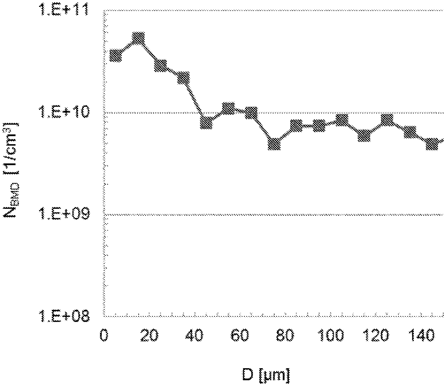
[0012] FIGS. 1, 3 and 4 each show the profile of the density of BMDs (N.sub.BMD) as a function of the distance (D) from the front side of an epitaxially coated semiconductor wafer which represents an example.
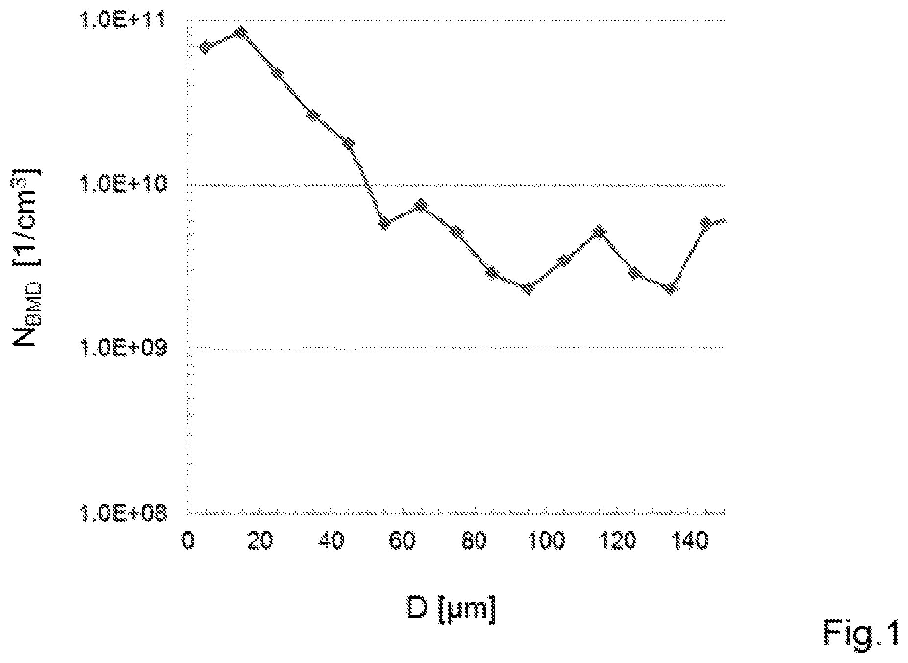
[0013] FIG. 2 shows the profile of the density of BMDs (N.sub.BMD) as a function of the distance (D) from the front side of an epitaxially coated semiconductor wafer which represents a comparative example.
DETAILED DESCRIPTION OF THE PREFERRED EMBODIMENTS
[0014] The substrate wafer contains an amount of boron sufficient to adjust the resistivity (the specific electrical resistance) to not less than 5 m.OMEGA.cm and not more than 10 m.OMEGA.cm. Preferably, the resistivity is not less than 6 m.OMEGA.cm and less than 10 m.OMEGA.cm.
[0015] The oxygen concentration of the substrate wafer is not less than 5.3.times.10.sup.17 atoms/cm.sup.3 and not more than 6.0.times.10.sup.17 atoms/cm.sup.3 (new ASTM).
[0016] The substrate wafer has not been deliberately doped with carbon and therefore contains preferably not more than 1.times.10.sup.16 atoms/cm.sup.3 of this element, more preferably not more than 1.times.10.sup.15 atoms/cm.sup.3. The substrate wafer has also not been deliberately doped with nitrogen and therefore preferably contains not more than 1.times.10.sup.12 atoms/cm.sup.3 of this element.
[0017] The thickness of the epitaxial layer is preferably not less than 1 .mu.m and not more than 5 .mu.m, more preferably 2 .mu.m to 3 .mu.m.
[0018] The epitaxially coated semiconductor wafer has a denuded zone, i.e. a region which extends from the front side into the interior and in which no BMDs are formed. The denuded zone has a thickness of preferably not less than 3 .mu.m and not more than 7 .mu.m.
[0019] The diameter of the epitaxially coated semiconductor wafer is not less than 200 mm, preferably not less than 300 mm.
[0020] The substrate wafer contains BMD nuclei which can be developed by a heat treatment to give BMDs. The heat treatment is preferably effected in a furnace and preferably in the course of the further processing of the epitaxially coated semiconductor wafer to give electronic components.
[0021] The heat treatment is conducted, for example, at a temperature of 850.degree. C. over a period of 1 h in oxygen or, for example, at a temperature of 900.degree. C. over a period of 30 min in argon, or is, for example, a two-stage heat treatment consisting of heating of the epitaxially coated semiconductor wafer to a temperature of 850.degree. C. over a period of 1 h and subsequently heating to a temperature of 1000.degree. C. over a period of 1 h in oxygen.
[0022] Irrespective of which of these three options is implemented, the substrate wafer of the epitaxially coated semiconductor wafer after the implemented heat treatment or a heat treatment with a comparable thermal budget has the following properties: the density of BMDs has a maximum of not less than 2.times.10.sup.10/cm.sup.3, and the distance of this maximum from the front side of the epitaxially coated semiconductor wafer is not more than 20 .mu.m. In addition, the quotient of the density of BMDs at a distance of 20 .mu.m from the front side and the density of BMDs at a distance of 60 .mu.m from the front side is not less than 5, where the surface of the epitaxial layer facing away from the substrate wafer forms the front side of the coated semiconductor wafer.
[0023] The profile of the density of BMDs from the front side into the interior of the epitaxially coated semiconductor wafer is preferably determined by counting defects with an optical microscope, specifically at a fracture edge of the epitaxially coated semiconductor wafer after preparation (delineation) of the BMDs by RIE (reactive ion etching). The preparation method by means of RIE has been described, for example, by Nakashima et al. in the Journal of The Electrochemical Society, 147 (11), 4294-4296 (2000).
[0024] The invention further provides a method of producing a p/p.sup.+ epitaxially coated semiconductor wafer of monocrystalline silicon, comprising:
the pulling of a single crystal of silicon at a pulling rate from a melt doped with boron and present in a crucible, where the concentration of oxygen in an envisaged section of the single crystal is not less than 5.3.times.10.sup.17 atoms/cm.sup.3 and not more than 6.0.times.10.sup.17 atoms/cm.sup.3 and the resistivity of the single crystal is not less than 5 m.OMEGA.cm and not more than 10 m.OMEGA.cm; the cooling of the single crystal within a first temperature range from 600.degree. C. to 500.degree. C., where the dwell time within the first temperature range is not less than 353 min and not more than 642 min, and the cooling of the single crystal within a second temperature range from 500.degree. C. to 400.degree. C., where the dwell time within the second temperature range is not less than 493 min and not more than 948 min; the dividing of a substrate wafer from the envisaged section of the cooled single crystal; and the depositing of a p-doped epitaxial layer of monocrystalline silicon on a polished upper side face of the substrate wafer.
[0025] The dwell time within the first temperature range is preferably not less than 353 min and not more than 514 min. The dwell time within the second temperature range is preferably not less than 493 min and not more than 759 min.
[0026] Within a third temperature range from 1000.degree. C. to 800.degree. C., the dwell time is preferably not less than 105 min and not more than 157 min.
[0027] There are important differences from the process described in DE 10 2014 221 421 B3. The melt is doped with a greater amount of boron, such that the resistivity of the single crystal is not less than 5 m.OMEGA.cm and not more than 10 m.OMEGA.cm, preferably not less than 6 m.OMEGA.cm and less than 10 m.OMEGA.cm.
[0028] In addition, in the cooling of the single crystal, it is ensured that the single crystal cools down comparatively slowly within the temperature range from 600.degree. C. to 500.degree. C. and within the temperature range from less than 500.degree. C. to 400.degree. C.
[0029] The single crystal can be cooled down, for example, in the presence of a water-cooled cooler. The dwell times envisaged may especially be established via the arrangement and the performance of the cooler and via the pulling rate with which the single crystal is pulled out of the melt. A favorable combination of arrangement, power and pulling rate can be discovered, for example, via simulation calculations. It is also possible to dispense with the cooler. In this case, the pulling rate necessary for the desired dwell times needs to be determined for a given configuration of the apparatus for pulling the single crystal.
[0030] The pulling rate is preferably not less than 0.4 mm/min and not more than 1.8 mm/min, this range being crucial particularly for pulling of single crystals having diameters of 200 mm, 300 mm or greater.
[0031] The melt is preferably subjected to a magnetic field. The magnetic field is preferably a horizontal magnetic field.
[0032] Deliberate doping of the melt with carbon or with nitrogen or with carbon and nitrogen is omitted.
[0033] As described, for example, in DE 10 2014 221 421 B3, the pulled single crystal is processed further to give substrate wafers of monocrystalline silicon, and the substrate wafers to give epitaxially coated semiconductor wafers. The operating steps preferably include the mechanical processing of a substrate wafer, for example the lapping and/or the grinding of the side faces of the substrate wafer, and the rounding of the edge of the substrate wafer. The substrate wafer is preferably also subjected to chemical etching and chemical-mechanical polishing. It therefore has a polished edge and at least one polished side face. Preferably, the upper and lower side faces are polished. The epitaxial layer of silicon is deposited on a polished side face. This step is preferably conducted in a single-wafer reactor, for example in a reactor of the Centura.RTM. type supplied by Applied Materials. The deposition gas preferably contains a hydrogen-containing silane, for example trichlorosilane (TCS), and a dopant-containing gas. The deposition temperature in the case of use of TCS is within a temperature range of preferably not less than 1000.degree. C. and not more than 1250.degree. C.
[0034] The deposition of the epitaxial layer is the first heat treatment of the substrate wafer, which is effected at a temperature of more than 700.degree. C.
[0035] The invention is described further hereinafter with reference to drawings and examples.
EXAMPLE
[0036] A single crystal of monocrystalline silicon was pulled by the CZ method at a pulling rate of 0.57 mm/min. The single crystal was cooled using a water-cooled cooler. The melt had been doped with boron only and had been subjected to a horizontal magnetic field. Details of dwell times (dt) with which the single crystal has been cooled within the crucial temperature intervals can be found in the table below. Substrate wafers divided from the single crystal with a diameter of 300 mm and a thickness of 775 .mu.m, an oxygen concentration of 5.7.times.10.sup.17/cm.sup.3 and a resistivity of 9 m.OMEGA.cm were processed further to give p/p.sup.+ epitaxially coated semiconductor wafers of silicon. The thickness of the epitaxial layer was 3 .mu.m.
[0037] The potential of such an epitaxially coated semiconductor wafer to be able to form BMDs was ascertained after the two-stage heat treatment (850.degree. C., 1 h and 1000.degree. C., 1 h, each in oxygen) of the epitaxially coated semiconductor wafer by means of RIE and defect counts in an optical microscope. An RIE system of the Plasmalab System 133 type from the manufacturer OXFORD INSTRUMENTS was used in conjunction with HBr, O.sub.2, Cl.sub.2 and Ar as gases for etching. At a pressure of 2 Pa and with an rf power of 350 W, etching was effected with a selectivity in the region of 1:100 (SiO.sub.2:Si).
[0038] FIG. 1 shows the profile of the density of BMDs (N.sub.BMD) as a function of the distance (D) from the front side of an epitaxially coated semiconductor wafer. Accordingly, there is a rise in the density of BMDs even at a comparatively small distance from the front side to a maximum of somewhat less than 1.times.10.sup.11/cm.sup.3, in order then to drop to values in the region of 5.times.10.sup.9/cm.sup.3 within a comparatively short distance.
COMPARATIVE EXAMPLE
[0039] A single crystal of monocrystalline silicon was pulled by the CZ method at a pulling rate of 0.57 mm/min. Details of dwell times (dt) with which the single crystal was cooled in particular temperature intervals can be found in the table below. Substrate wafers divided from the single crystal with a diameter of 300 mm and a thickness of 775 .mu.m, an oxygen concentration of 5.5.times.10.sup.17/cm.sup.3 and a resistivity of 8 m.OMEGA.cm were processed further to give p/p.sup.+ epitaxially coated semiconductor wafers of silicon. The thickness of the epitaxial layer was 3 .mu.m.
[0040] The potential of such an epitaxially coated semiconductor wafer to be able to form BMDs was ascertained after the two-stage heat treatment (850.degree. C., 1 h and 1000.degree. C., 1 h, each in oxygen) of the epitaxially coated semiconductor wafer by means of RIE and defect counts in an optical microscope.
[0041] FIG. 2 shows the profile of the density of BMDs (N.sub.BMD) as a function of the distance (D) from the front side of an epitaxially coated semiconductor wafer. Accordingly, no maximum of BMDs with the required property is obtained close to the front side and the density of BMDs remains clearly below 1.times.10.sup.10/cm.sup.3.
TABLE-US-00001 TABLE dt 1000.degree. C.- dt 700.degree. C.- dt 600.degree. C.- dt 500.degree. C.- 800.degree. C. 600.degree. C. 500.degree. C. 400.degree. C. (min) (min) (min) (min) Example 147 218.5 390.5 562.5 Comparative 365 255 285 400 example
[0042] The data show that the dwell time in the temperature ranges from 600.degree. C. onward is of particular significance. It must be comparatively long in order that the desired BMD profile can develop.
[0043] A similar profile of BMD densities is also obtained when, instead of the two-stage heat treatment, one of the above-described heat treatments is conducted.
[0044] FIG. 3 shows the profile of the density of BMDs (N.sub.BMD) as a function of the distance (D) from the front side of a semiconductor wafer epitaxially coated according to the example after a heat treatment in a furnace at a temperature of 850.degree. C. in oxygen over a period of 1 h.
[0045] FIG. 4 shows the profile of the density of BMDs (N.sub.BMD) as a function of the distance (D) from the front side of a semiconductor wafer epitaxially coated according to the example after a heat treatment in a furnace at a temperature of 900.degree. C. in argon over a period of 30 min.
[0046] The above description of illustrative embodiments should be regarded as an illustration. The disclosure that has thus been made enables the person skilled in the art firstly to understand the present invention and the associated advantages, and secondly encompasses, within the understanding of the person skilled in the art, obvious alterations and modifications to the structures and methods described as well.
[0047] Therefore, all such alterations and modifications and equivalents shall be covered by the scope of protection of the claims.
* * * * *
D00000
D00001
D00002
D00003
D00004
XML
uspto.report is an independent third-party trademark research tool that is not affiliated, endorsed, or sponsored by the United States Patent and Trademark Office (USPTO) or any other governmental organization. The information provided by uspto.report is based on publicly available data at the time of writing and is intended for informational purposes only.
While we strive to provide accurate and up-to-date information, we do not guarantee the accuracy, completeness, reliability, or suitability of the information displayed on this site. The use of this site is at your own risk. Any reliance you place on such information is therefore strictly at your own risk.
All official trademark data, including owner information, should be verified by visiting the official USPTO website at www.uspto.gov. This site is not intended to replace professional legal advice and should not be used as a substitute for consulting with a legal professional who is knowledgeable about trademark law.