Siltronic AG

USPTO Trademark & Patent Filings

Siltronic Ag

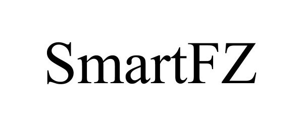
Trademark applications and grants for Siltronic Ag. Siltronic Ag has 11 trademark applications. The latest application filed is for "SMARTFZ"

Company Profile
    Company Aliases
  • SILTRONIC AG
  • ag siltronic
  • Siltronic AG - Munich DE
  • SILTRONIC AG - Munich DE
State Incorporated GERMANY
Entity Type JOINT STOCK COMPANY
Address Einsteinstr. 172 München GERMANY 81677

*profile and listings may contain filings by different individuals or companies with the same name. Review application materials to confirm ownership/assignment.
Trademarks Patents
Patent Applications
Patent ApplicationDate
METHOD FOR PRODUCING SEMICONDUCTOR WAFERS FROM MONOCRYSTALLINE SILICON
20220298670 - 17/636370 Heuwieser; Walter ;   et al.
2022-09-22
METHOD FOR DEPOSITING AN EPITAXIAL LAYER ON A FRONT SIDE OF A SEMICONDUCTOR WAFER, AND DEVICE FOR CARRYING OUT THE METHOD
20220267926 - 17/614214 HABERECHT; Joerg ;   et al.
2022-08-25
METHOD FOR PULLING A SINGLE CRYSTAL OF SILICON IN ACCORDANCE WITH THE CZOCHRALSKI METHOD
20220259762 - 17/625268 MANGELBERGER; Karl ;   et al.
2022-08-18
INSTALLATION AND METHOD FOR POLISHING SEMICONDUCTOR WAFERS
20220258303 - 17/618746 FRANKE; Jonny ;   et al.
2022-08-18
METHOD FOR PRODUCING SEMICONDUCTOR WAFERS
20220236205 - 17/612603 BOY; Michael ;   et al.
2022-07-28
Single crystal of silicon with <100> orientation, which is doped with n-type dopant, and method for producing such a single crystal
11,390,962 - 16/643,673 Raming , et al. July 19, 2
2022-07-19
Single crystal of silicon with <100> orientation, which is doped with n-type dopant, and method for producing such a single crystal
11,390,962 - 16/643,673 Raming , et al. July 19, 2
2022-07-19
Susceptor for holding a semiconductor wafer having an orientation notch, a method for depositing a layer on a semiconductor wafer, and semiconductor wafer
11,380,621 - 15/928,534 Schauer , et al. July 5, 2
2022-07-05
Susceptor for holding a semiconductor wafer having an orientation notch, a method for depositing a layer on a semiconductor wafer, and semiconductor wafer
11,380,621 - 15/928,534 Schauer , et al. July 5, 2
2022-07-05
Device for handling a semiconductor wafer in an epitaxy reactor and method for producing a semiconductor wafer having an epitaxial layer
11,302,565 - 16/309,014 Moos , et al. April 12, 2
2022-04-12
Patent Grants & Applications

uspto.report is an independent third-party trademark research tool that is not affiliated, endorsed, or sponsored by the United States Patent and Trademark Office (USPTO) or any other governmental organization. The information provided by uspto.report is based on publicly available data at the time of writing and is intended for informational purposes only.

While we strive to provide accurate and up-to-date information, we do not guarantee the accuracy, completeness, reliability, or suitability of the information displayed on this site. The use of this site is at your own risk. Any reliance you place on such information is therefore strictly at your own risk.

All official trademark data, including owner information, should be verified by visiting the official USPTO website at www.uspto.gov. This site is not intended to replace professional legal advice and should not be used as a substitute for consulting with a legal professional who is knowledgeable about trademark law.

© 2024 USPTO.report | Privacy Policy | Resources | RSS Feed of Trademarks | Trademark Filings Twitter Feed