Substrate Supporting Unit And A Substrate Processing Device Including The Same
Lee; SeungHwan ; et al.
U.S. patent application number 16/671847 was filed with the patent office on 2020-05-07 for substrate supporting unit and a substrate processing device including the same. The applicant listed for this patent is ASM IP Holding B.V.. Invention is credited to JongSu Kim, SungBae Kim, HakYong Kwon, SeungHwan Lee, JuHyuk Park.
| Application Number | 20200141003 16/671847 |
| Document ID | / |
| Family ID | 70459629 |
| Filed Date | 2020-05-07 |


| United States Patent Application | 20200141003 |
| Kind Code | A1 |
| Lee; SeungHwan ; et al. | May 7, 2020 |
SUBSTRATE SUPPORTING UNIT AND A SUBSTRATE PROCESSING DEVICE INCLUDING THE SAME
Abstract
A substrate processing device capable of preventing deformation of a substrate during a process includes a substrate supporting unit having a contact surface that comes into contact with an edge of a substrate to be processed, wherein the substrate supporting unit includes a protruding (e.g. embossed) structure protruding from a base to support deformation from the inside of the edge of the substrate to be processed.
| Inventors: | Lee; SeungHwan; (Anseong-si, KR) ; Kwon; HakYong; (Hwaseong-si, KR) ; Kim; JongSu; (Hwaseong-si, KR) ; Kim; SungBae; (Cheonan-si, KR) ; Park; JuHyuk; (Asan-si, KR) | ||||||||||
| Applicant: |
|
||||||||||
|---|---|---|---|---|---|---|---|---|---|---|---|
| Family ID: | 70459629 | ||||||||||
| Appl. No.: | 16/671847 | ||||||||||
| Filed: | November 1, 2019 |
| Current U.S. Class: | 1/1 |
| Current CPC Class: | H01J 37/32082 20130101; H01L 21/673 20130101; C23C 16/45536 20130101; H01L 21/67017 20130101; H01L 21/68735 20130101; C23C 16/45544 20130101; C23C 16/458 20130101; H01L 21/6875 20130101; H01L 21/6838 20130101 |
| International Class: | C23C 16/455 20060101 C23C016/455; C23C 16/458 20060101 C23C016/458; H01L 21/67 20060101 H01L021/67; H01L 21/673 20060101 H01L021/673; H01J 37/32 20060101 H01J037/32 |
Foreign Application Data
| Date | Code | Application Number |
|---|---|---|
| Nov 2, 2018 | KR | 10-2018-0133838 |
Claims
1. A substrate processing device comprising: a gas supply unit; and a substrate supporting unit below the gas supply unit, wherein the substrate supporting unit comprises: a base; a first protrusion adjacent to a periphery of the base and protruding to a first height; and a second protrusion adjacent to a center of the base and protruding to a second height less than the first height.
2. The substrate processing device of claim 1, wherein the second protrusion comprises a conductive material.
3. The substrate processing device of claim 2, wherein the second protrusion is electrically connected to ground.
4. The substrate processing device of claim 2, wherein the second protrusion is electrically connected to a radio frequency (RF) power supply.
5. The substrate processing device of claim 1, further comprising: a heater block below the substrate supporting unit, wherein a positioning hole is formed in the center of the base, and a position fixing pin is inserted into the positioning hole and a position of the base with respect to the heater block is fixed.
6. The substrate processing device of claim 5, wherein a plurality of second protrusions are symmetrically distributed with respect to the positioning hole.
7. The substrate processing device of claim 1, wherein the first protrusion comprises a contact surface that comes into contact with an edge of a substrate to be processed.
8. The substrate processing device of claim 7, further comprising: a suction force generator generating a suction force such that a backside of the substrate to be processed faces the base.
9. The substrate processing device of claim 8, wherein the substrate to be processed is deformed due to the suction force, and the second protrusion supports the substrate to be processed during the deformation.
10. The substrate processing device of claim 1, wherein the substrate to be processed is deformed due to a temperature change of the substrate processing device, and the second protrusion supports the substrate to be processed during the deformation.
11. The substrate processing device of claim 1, wherein active species are formed when an electric power is supplied between the gas supply unit and the substrate supporting unit to form an electric field, and the active species are distributed adjacent to the second protrusion by an electric field concentrated on the second protrusion.
12. A substrate supporting unit configured to accommodate a substrate, the substrate supporting unit comprising: a base; a first protrusion protruding from the base to a first height; and a second protrusion protruding from the base to a second height less than the first height, wherein the first protrusion surrounds the second protrusion.
13. The substrate supporting unit of claim 12, wherein the base comprises a first region corresponding to an edge of the substrate, and the first protrusion is adjacent to the first region.
14. The substrate supporting unit of claim 13, wherein the base further comprises a second region corresponding to a center of the substrate, and the second protrusion is adjacent to the second region.
15. A substrate processing device comprising: a substrate supporting unit having a contact surface that comes into contact with an edge of a substrate to be processed, wherein the substrate supporting unit is configured to support deformation from the inside of the edge of the substrate to be processed.
16. The substrate processing device of claim 15, wherein the substrate supporting unit is an edge-contact susceptor (ECS).
17. The substrate processing device of claim 15, wherein the substrate supporting unit comprises: a first protrusion having the contact surface; and a second protrusion supporting the deformation.
18. The substrate processing device of claim 17, wherein the second protrusion has a lower upper surface than an upper surface of the first protrusion.
19. The substrate processing device of claim 15, wherein the substrate supporting unit is configured such that active species arranged on the substrate to be processed are arranged around a center of the substrate to be processed.
20. The substrate processing device of claim 19, wherein the substrate supporting unit comprises: a first protrusion having the contact surface; and a second protrusion affecting an arrangement of the active species.
Description
CROSS-REFERENCE TO RELATED APPLICATION
[0001] This application claims the benefit of Korean Patent Application No. 10-2018-0133838, filed on Nov. 2, 2018, in the Korean Intellectual Property Office, the disclosure of which is incorporated herein in its entirety by reference.
BACKGROUND
1. Field
[0002] One or more embodiments relate to a substrate supporting unit and a substrate processing device including the same, and more particularly, to a substrate supporting unit capable of preventing deformation of a substrate and realizing a symmetrical thin-film profile, and a substrate processing device including the substrate supporting unit.
2. Description of the Related Art
[0003] The size of a semiconductor device is continuously shrinked, and accordingly, the importance of precise control of a thin film processed (e.g., deposited) on a substrate is also increasing. As an example of the precise control, atomic layer deposition (ALD) has been used as a technique to realize the precise control of the thin film in which atomic layer-sized thin films are formed layer-by-layer by sequentially and alternately supplying two or more reactive gases onto the substrate.
[0004] Through such an atomic layer deposition process, thin films may be uniformly and precisely deposited on the surface of a substrate having a complicated step structure. Further, by applying a plasma atomic layer deposition process in which at least one reactive gas is excited by plasma, a thin film may be deposited at a lower temperature, thereby improving the reliability of a semiconductor device.
[0005] Meanwhile, in a plasma process, it is very important to generate plasma uniformly on a substrate. In order to generate uniform plasma in a reaction space on the substrate, it is preferable to arrange a radio frequency (RF) rod for supplying an RF current at the center of an upper electrode, for example, an upper surface of a showerhead. However, due to mutual physical interference by a gas supply port at the center of the upper surface of the showerhead, the arrangement of such an RF rod is substantially difficult.
SUMMARY
[0006] One or more embodiments include a device capable of overcoming the difficulty of disposing the RF rod at the center portion of the upper electrode described above to create uniform plasma on a substrate and deposit a uniform thin film.
[0007] One or more embodiments include a device capable of preventing excessive deformation of a substrate that may occur during use of an edge-contact susceptor (ECS).
[0008] Additional aspects will be set forth in part in the description which follows and, in part, will be apparent from the description, or may be learned by practice of the presented embodiments.
[0009] According to one or more embodiments, a substrate processing device includes: a gas supply unit; and a substrate supporting unit below the gas supply unit, wherein the substrate supporting unit includes: a base; a first protrusion adjacent to a periphery of the base and protruding to a first height; and a second protrusion adjacent to a center of the base and protruding to a second height less than the first height.
[0010] The second protrusion may include a conductive material. The second protrusion may be electrically connected to ground. The second protrusion may be electrically connected to a radio frequency (RF) power supply.
[0011] The substrate processing device may further include: a heater block below the substrate supporting unit, wherein a positioning hole may be formed in the center of the base, and a position fixing pin may be inserted into the positioning hole and a position of the base with respect to the heater block is fixed.
[0012] A plurality of second protrusions may be symmetrically distributed with respect to the positioning hole.
[0013] The first protrusion may include a contact surface that comes into contact with an edge of a substrate to be processed.
[0014] The substrate processing device may further include: a suction force generator generating a suction force such that a backside of the substrate to be processed faces the base.
[0015] The substrate to be processed may be deformed due to the suction force, and the second protrusion may support the substrate to be processed during the deformation.
[0016] The substrate to be processed may be deformed due to a temperature change of the substrate processing device, and the second protrusion may support the substrate to be processed during the deformation.
[0017] Active species may be formed when an RF power is supplied between the gas supply unit and the substrate supporting unit, and the active species may be distributed adjacent to the second protrusion by an electric field concentrated on the second protrusion.
[0018] According to one or more embodiments, a substrate supporting unit configured to accommodate a substrate includes: a base; a first protrusion protruding from the base to a first height; and a second protrusion protruding from the base to a second height less than the first height, wherein the first protrusion surrounds the second protrusion.
[0019] The base may include a first region corresponding to an edge of the substrate, and the first protrusion may be adjacent to the first region.
[0020] The base may further include a second region corresponding to a center of the substrate, and the second protrusion may be adjacent to the second region.
[0021] According to one or more embodiments, a substrate processing device includes: a substrate supporting unit having a contact surface that comes into contact with an edge of a substrate to be processed, wherein the substrate supporting unit is configured to support deformation inside the edge of the substrate to be processed.
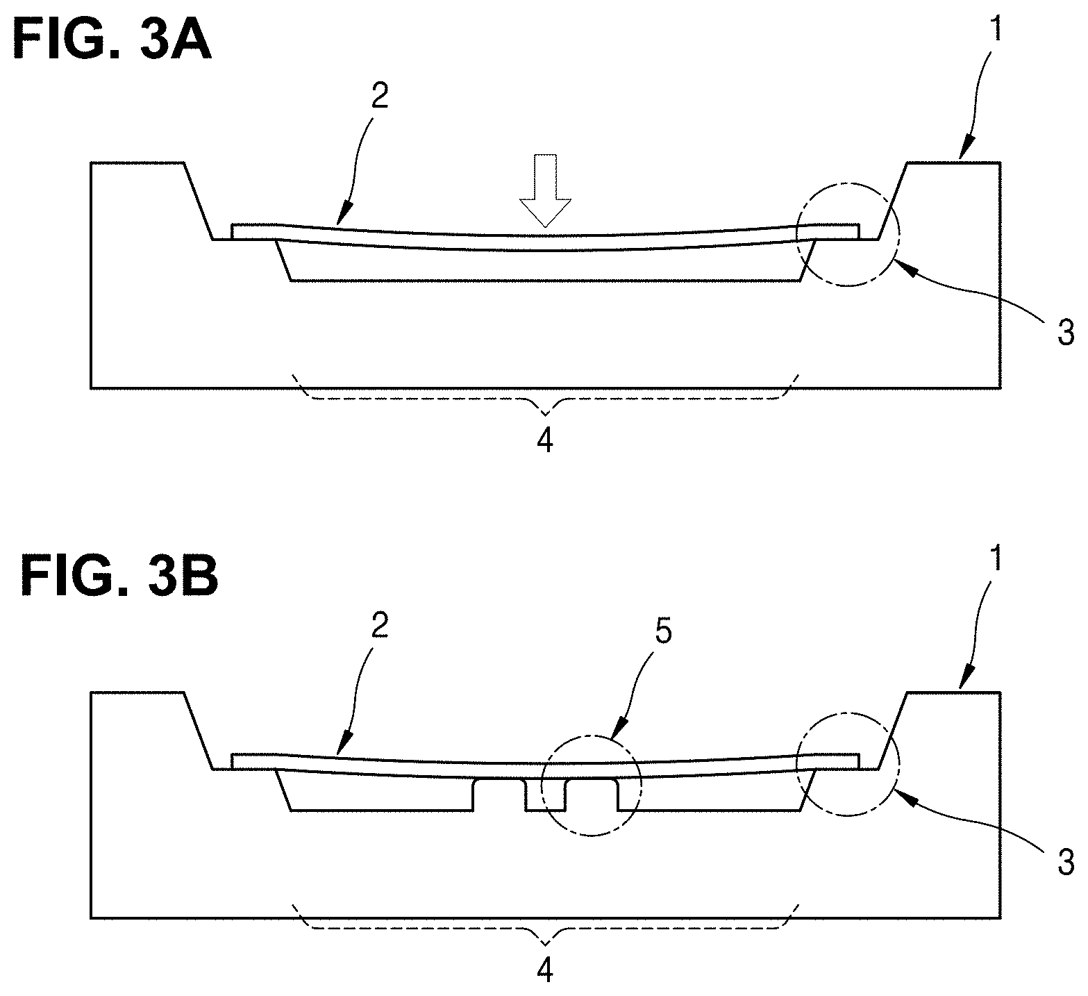
[0022] The substrate supporting unit may be an ECS.
[0023] The substrate supporting unit may include: a first protrusion having the contact surface; and a second protrusion supporting the deformation.
[0024] The second protrusion may have a lower upper surface than an upper surface of the first protrusion.
[0025] The substrate supporting unit may be configured such that active species arranged on the substrate to be processed are arranged around a center of the substrate to be processed.
[0026] The substrate supporting unit may include: a first protrusion having the contact surface; and a second protrusion affecting an arrangement of the active species.
BRIEF DESCRIPTION OF THE DRAWINGS
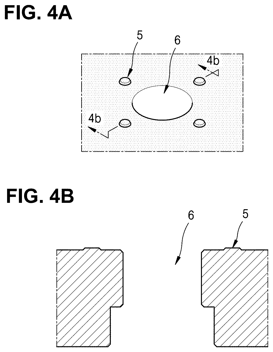
[0027] These and/or other aspects will become apparent and more readily appreciated from the following description of the embodiments, taken in conjunction with the accompanying drawings in which:
[0028] FIGS. 1 and 2 are views of substrate processing devices according to embodiments;
[0029] FIGS. 3A and 3B are views of substrate supporting units. FIG. 3A is a view of a conventional supporting unit. FIG. 3B is a view of a substrate supporting unit according to embodiments;
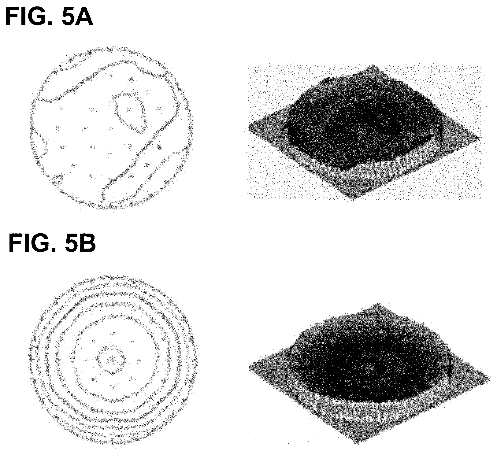
[0030] FIGS. 4A and 4B are views of substrate supporting units according to embodiments;
[0031] FIGS. 5A and 5B show a thin-film profile when a SiO2 thin film is deposited on a substrate mounted on the substrate processing device of FIG. 1, by a plasma atomic layer deposition (PEALD) method; and
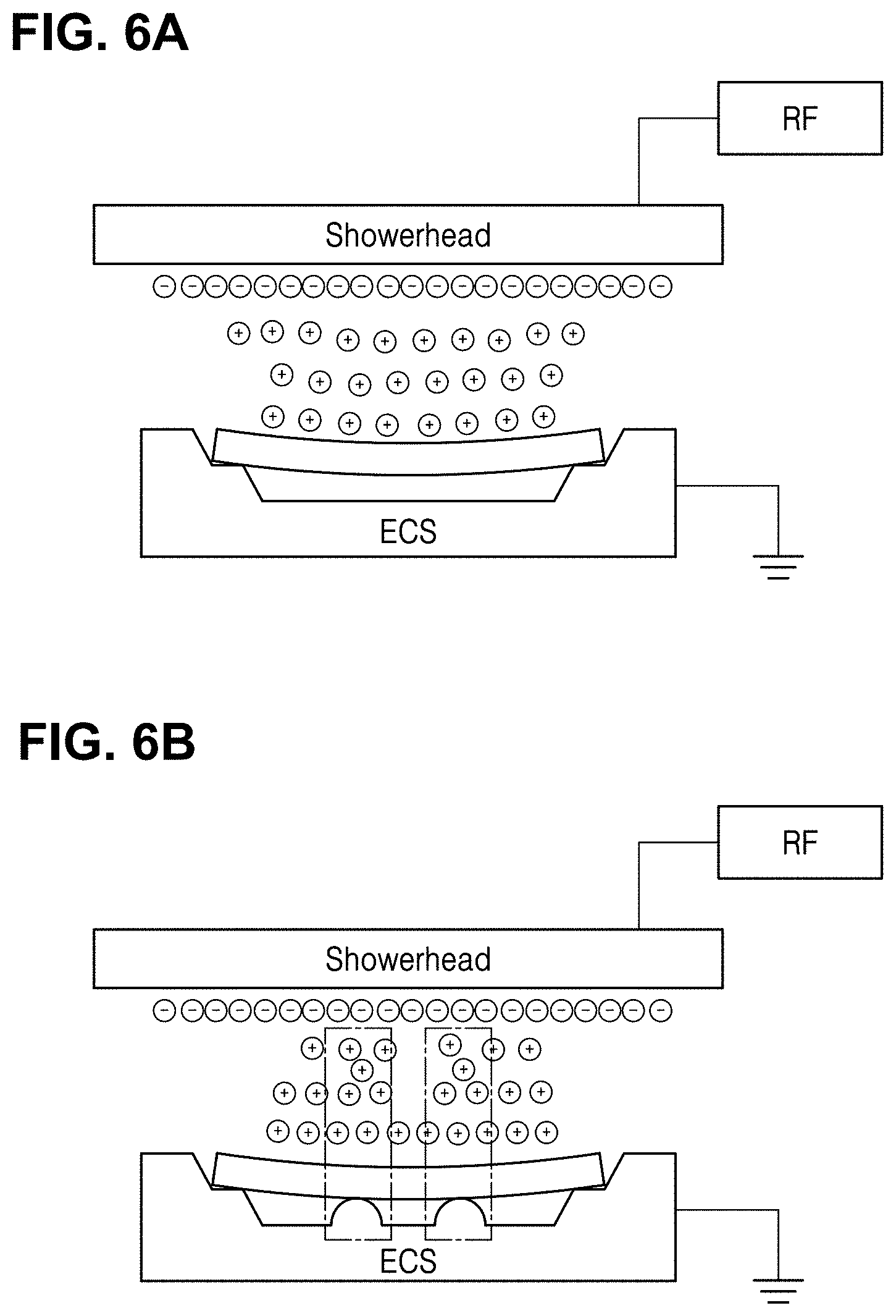
[0032] FIGS. 6A and 6B are views showing the density of charges around embossings according to the polarity of electrodes; and
[0033] FIGS. 7A and 7B are views showing the density of charges around embossings according to the polarity of electrodes.
DETAILED DESCRIPTION
[0034] Hereinafter, one or more embodiments will be described more fully with reference to the accompanying drawings.
[0035] In this regard, the present embodiments may have different forms and should not be construed as being limited to the descriptions set forth herein. Rather, these embodiments are provided so that the present disclosure will be thorough and complete, and will fully convey the scope of the present disclosure to one of ordinary skill in the art.
[0036] The terminology used herein is for the purpose of describing particular embodiments and is not intended to limit the present disclosure. As used herein, the singular forms "a", "an", and "the" are intended to include the plural forms as well, unless the context clearly indicates otherwise. It will be further understood that the terms "includes", "comprises" and/or "including", "comprising" used herein specify the presence of stated features, integers, steps, operations, members, components, and/or groups thereof, but do not preclude the presence or addition of one or more other features, integers, steps, operations, members, components, and/or groups thereof. As used herein, the term "and/or" includes any and all combinations of one or more of the associated listed items. Expressions such as "at least one of," when preceding a list of elements, modify the entire list of elements and do not modify the individual elements of the list
[0037] It will be understood that, although the terms first, second, etc. may be used herein to describe various members, components, regions, layers, and/or sections, these members, components, regions, layers, and/or sections should not be limited by these terms. These terms do not denote any order, quantity, or importance, but rather are only used to distinguish one component, region, layer, and/or section from another component, region, layer, and/or section. Thus, a first member, component, region, layer, or section discussed below could be termed a second member, component, region, layer, or section without departing from the teachings of embodiments.
[0038] In the present disclosure, "gas" may include evaporated solids and/or liquids and may include a single gas or a mixture of gases. In the present disclosure, the process gas introduced into a reaction chamber through a gas supply unit may include a precursor gas and an additive gas. The precursor gas and the additive gas may typically be introduced as a mixed gas or may be separately introduced into a reaction space. The precursor gas may be introduced together with a carrier gas such as an inert gas. The additive gas may include a dilution gas such as a reactant gas and an inert gas. The reactant gas and the dilution gas may be mixedly or separately introduced into the reaction space. The precursor may include two or more precursors, and the reactant gas may include two or more reactant gases. The precursor may be a gas that is chemisorbed onto a substrate and typically contains metalloid or metal elements constituting a main structure of a matrix of a dielectric film, and the reactant gas for deposition may be a gas that reacts with the precursor chemisorbed onto the substrate when excited to fix an atomic layer or a monolayer on the substrate. The term "chemisorption" may refer to chemical saturation adsorption. A gas other than the process gas, that is, a gas introduced without passing through the gas supply unit, may be used to seal the reaction space, and it may include a seal gas such as an inert gas. In some embodiments, the term "film" may refer to a layer that extends continuously in a direction perpendicular to a thickness direction without substantially having pinholes to cover an entire target or a relevant surface, or may refer to a layer that simply covers a target or a relevant surface. In some embodiments, the term "layer" may refer to a structure, or a synonym of a film, or a non-film structure having any thickness formed on a surface. The film or layer may include a discrete single film or layer or multiple films or layers having some characteristics, and the boundary between adjacent films or layers may be clear or unclear and may be set based on physical, chemical, and/or some other characteristics, formation processes or sequences, and/or functions or purposes of the adjacent films or layers.
[0039] In the present disclosure, the expression "same material" should be interpreted as meaning that main components (constituents) are the same. For example, when a first layer and a second layer are both silicon nitride layers and are formed of the same material, the first layer may be selected from the group consisting of Si2N, SiN, Si3N4, and Si2N3 and the second layer may also be selected from the above group but a particular film quality thereof may be different from that of the first layer.
[0040] Additionally, in the present disclosure, according as an operable range may be determined based on a regular job, any two variables may constitute an operable range of the variable and any indicated range may include or exclude end points. Additionally, the values of any indicated variables may refer to exact values or approximate values (regardless of whether they are indicated as "about"), may include equivalents, and may refer to an average value, a median value, a representative value, a majority value, or the like.
[0041] In the present disclosure where conditions and/or structures are not specified, those of ordinary skill in the art may easily provide these conditions and/or structures as a matter of customary experiment in the light of the present disclosure. In all described embodiments, any component used in an embodiment may be replaced with any equivalent component thereof, including those explicitly, necessarily, or essentially described herein, for intended purposes, and in addition, the present disclosure may be similarly applied to devices and methods.
[0042] Hereinafter, embodiments of the present disclosure will be described with reference to the accompanying drawings. In the drawings, variations from the illustrated shapes may be expected as a result of, for example, manufacturing techniques and/or tolerances. Thus, the embodiments of the present disclosure should not be construed as being limited to the particular shapes of regions illustrated herein but may include deviations in shapes that result, for example, from manufacturing processes.
[0043] FIG. 1 schematically shows a substrate processing device according to embodiments. Although a deposition device or an etching device of a semiconductor or a display substrate is described herein as the substrate processing device, it is to be understood that the present disclosure is not limited thereto. The substrate processing device may be any device necessary for processing a substrate.
[0044] Referring to FIG. 1, the substrate processing device may include a reactor wall 110, a gas supply unit 120, a substrate supporting unit 130, a heater block H, an exhaust passage 140, and an RF rod 130.
[0045] The reactor wall 110 may be a component of a reactor in the substrate processing device. In other words, a reaction space for deposition of the substrate may be formed by the reactor wall 110. For example, the reactor wall 110 may include a sidewall and/or upper wall of the reactor. The upper wall of the reactor in the reactor wall 110 may provide a gas supply channel 150 through which source gas, purge gas, and/or reaction gas may be supplied.
[0046] The gas supply unit 120 may be on the substrate supporting unit 130. The gas supply unit 120 may be connected to the gas supply channel 150. The gas supply unit 120 may be fixed to the reactor. For example, the gas supply unit 120 may be fixed to the reactor wall 110 via a fixing member (not shown). The gas supply unit 120 may be configured to supply gas to an object to be processed in a reaction space 160. For example, the gas supply unit 120 may be a showerhead assembly.
[0047] A gas flow channel 170 communicating with the gas supply channel 150 may be formed in the gas supply unit 120. The gas flow channel 170 may be formed between a gas channel 125 (upper portion) of the gas supply unit 120 and a gas supply plate 127 (lower portion) of the gas supply unit 120. Although the gas channel 125 and the gas supply plate 127 are shown as separate structures in the drawings, the gas channel 125 and the gas supply plate 127 may be formed in an integrated structure.
[0048] The substrate supporting unit 130 may be under the gas supply unit 120. The substrate supporting unit 130 may perform a function of supporting a substrate S to be processed. Further, the substrate supporting unit 130 may function as an electrode. For example, an RF power may be transferred to the reaction space 160 through the substrate supporting unit 130, thereby forming plasma in the reaction space.
[0049] By the RF power supplied through the substrate supporting unit 130, a potential (e.g., a negative potential) may be formed on a substrate exposed in the reaction space. For example, the substrate supporting unit 130 may be connected to a plasma generation unit (not shown), and an RF power generated by the plasma generation unit may be supplied to the substrate S to be processed in the reaction space by the substrate supporting unit 130. As a result, plasma may be formed in the reaction space between the substrate supporting unit 130 and the gas supply unit 120.
[0050] The substrate supporting unit 130 may be configured to contact a lower surface of the reactor wall 110 to form a reaction space. To this end, the substrate supporting unit 130 may include a sealing surface C1 that is in contact with the lower surface of the reactor wall 110. Furthermore, the substrate supporting unit 130 may be configured to provide a space to which the substrate S to be processed is stably loaded. To this end, the substrate supporting unit 130 may include a contact surface C2 that comes into contact with an edge of the substrate S to be processed. In an alternative embodiment, the sealing surface C1 and the contact surface C2 may be formed at different levels. In some embodiments, the substrate supporting unit 130 may be an edge-contact susceptor (ECS).
[0051] In some embodiments, the substrate supporting unit 130 may include a first protrusion P1 that provides at least one of the sealing surface C1 and the contact surface C2. The first protrusion P1 may protrude adjacent to the periphery of a base B of the substrate supporting unit 130. The first protrusion P1 may protrude to a first height. The first height may be a height from the base B to the contact surface C2. In other words, the first height may be defined as the same height as a rear surface of the substrate S to be processed which is loaded on the substrate supporting unit 130.
[0052] The first protrusion P1 may include the same material as that of the base B. For example, when the base B includes a metal (e.g., aluminum), the first protrusion P1 may also include a metal (e.g., aluminum). In another embodiment, the first protrusion P1 may include a material different from that of the base B. For example, the base B may include a metal, while the first protrusion P1 may include ceramics.
[0053] A first portion of the first protrusion P1 may include the contact surface C2 that comes into contact with the edge of the substrate S to be processed. A surface of the substrate S to be processed and a surface of the first protrusion P1 may contact each other through the contact surface C2.
[0054] In an alternative embodiment, when a width of the contact surface contacting the substrate S is less than or equal to a certain threshold value, the contact surface C2 contacting the substrate S may also be referred to as a contact line. When such a contact line is formed, it is defined that two faces are in line contact. Such a contact line by the line contact may have a form of ring corresponding to the substrate S to be processed having a thin thickness (e.g., a continuous/non-continuous ring type). Alternatively, the line contact may occur at a corner portion of the first protrusion P1.
[0055] A second portion of the first protrusion P1 may include the sealing surface C1 that comes into contact with the lower surface of the reactor wall 110. A reaction space may be formed by coupling the reactor wall 110 and the first protrusion P1 through the sealing surface C1. In an embodiment, the sealing surface C1 and the contact surface C2 may be formed at an identical level. That is, the sealing surface C1 and the contact surface C2 may be formed on an identical plane.
[0056] In another embodiment, the sealing surface C1 and the contact surface C2 may be formed at different levels. That is, the sealing surface C1 and the contact surface C2 may be formed on different planes. For example, as shown in FIG. 1, the sealing surface C1 may be formed at a level higher than the contact surface C2, or the sealing surface C1 may be formed at a level lower than the contact surface C2.
[0057] The substrate supporting unit 130 may be configured to support deformation from the inside of the edge (e.g., a center of the substrate S) of the substrate S to be processed. To this end, the substrate supporting unit 130 may further include a second protrusion P2 different from the first protrusion P1. The second protrusion P2 may be disposed in the inner portion of the substrate supporting unit 130 compared to first protrusion P1. In other words, the first protrusion P1 may surround the second protrusion P2 in a horizontal direction (i.e., a direction in which the base B extends).
[0058] The second protrusion P2 may be adjacent to the center of the base B. That is, the second protrusion P2 may be closer to the center (e.g., the center of the base B) between the center and an edge of the base B. For example, when the base B includes a first region corresponding to an edge of the substrate and a second region corresponding to the center of the substrate, the first protrusion P1 may be adjacent to the first region and the second protrusion P2 may be adjacent to the second region.
[0059] The second protrusion P2 may include the same material as that of the base B or may include a material different from that of the base B. For example, when the base B is a metal (e.g., aluminum), the first protrusion P1 may also include a metal (e.g., aluminum). In another embodiment, the base B may include a metal, while the second protrusion P2 may include ceramics. In another embodiment, the base B may include ceramics, while the second protrusion P2 may include a metal.
[0060] The second protrusion P2 may be configured to support deformation of the substrate (e.g., deformation of the substrate in a direction of the base B). To this end, the second protrusion P2 may protrude to have a lower height than the first protrusion P1. The height may be defined as a height lower than the rear surface of the substrate S to be processed. Since the second protrusion P2 has an upper surface lower than an upper surface of the first protrusion P1 (i.e., the contact surface C2), the substrate may be supported by the second protrusion P2 when the substrate is bent downward due to a temperature change, gravity, and/or suction force.
[0061] In more detail, the substrate S to be processed may be deformed due to a temperature change of the substrate processing device. In this case, the second protrusion P2 may support the substrate S to be processed during deformation due to the temperature change. In another example, suction force may be generated by a suction force generator to be included in the substrate processing device, thereby causing deformation of the substrate S to be processed. For example, the suction force may be generated such that a backside of the substrate S to be processed faces the base B, and in this case, the substrate S to be processed may be bent in the direction of the base B. In this case, the second protrusion P2 may support the substrate S to be processed during deformation due to the suction force.
[0062] As such, when the substrate S to be processed is deformed to have a certain curvature toward the base B under a certain temperature and/or suction force, the deformed substrate may be in line contact with the first protrusion P1 and at the same time in contact with the second protrusion P2. Accordingly, the line contact of the substrate S to be processed by the first protrusion P1 is maintained to prevent flow of reactive gas into the rear surface of the substrate S, and excessive bending (deformation) of the substrate may be prevented by the second protrusion P2.
[0063] In addition to the above-described support function, the second protrusion P2 may also function to relocate active species in the reaction space. To this end, the second protrusion P2 may include a conductive material. In an embodiment, the second protrusion P2 may be electrically connected to ground (see FIG. 6). In another embodiment, the second protrusion P2 may be electrically connected to a radio frequency (RF) power supply (see FIG. 7).
[0064] During a plasma process, an electric power (e.g., RF power) may be supplied between the gas supply unit 120 and the substrate supporting unit 130, and active species may be formed by the power. Meanwhile, in a case of a substrate supporting unit 130 to which an electric power, e.g. RF power is supplied, an electric field may be concentrated on the second protrusion P2 including a conductive material. Due to the concentration of such the electric field, the active species arranged on the substrate S to be processed may be distributed adjacent to the second protrusion P2. The second protrusion P2 is adjacent to the center of the base B so that the active species may be arranged around the center of the substrate S to be processed. Thus, substrate processing by the active species may be performed symmetrically around the center of the substrate S to be processed. As such, the second protrusion P2 may be affecting an arrangement of the active species.
[0065] In an alternative embodiment, a plurality of second protrusions P2 may be arranged symmetrically around the center of the substrate supporting unit 130, for symmetrical arrangement of the active species. The second protrusions P2 may be in a non-continuous form (e.g., in the form of embossing) or may be in a continuous form (e.g., in the form of a ring). Although not shown in the drawings, the second protrusions P2 may be arranged at the center of the base B. That is, the second protrusions P2 may be arranged such that the center of symmetry of the second protrusions P2 and the center of the base B coincide with each other.
[0066] As such, according to embodiments of the present disclosure, excessive deformation of the substrate may be prevented in vacuum suction and high temperature processes by forming a protrusion in a central portion of an ECS pedestal. Further, a thin-film processing process having a more symmetrical thin-film profile in the plasma process may be performed.
[0067] Referring again to FIG. 1, the substrate supporting unit 130 may be supported by a body 200, and the body 200 may be moved up and down and rotated. The substrate supporting unit 130 is separated from the reactor wall 110 or brought into contact with the reactor wall 110 by the up and down movement of the body 200 so that the reaction space 160 may be opened or closed. Processing (e.g., deposition, etching, etc.) on the substrate may be performed in the reaction space 160.
[0068] Gas and/or reaction residues and the like supplied through the gas supply unit 120 for treatment may be exhausted through the exhaust passage 140. For example, the exhaust passage 140 may be connected to an exhaust pump (not shown), and the gas and/or reaction residues may be exhausted by the exhaust units. It should be noted that although the exhaust passage 140 of an upstream exhaust structure is shown in the drawings, the present disclosure is not limited thereto. In other words, an exhaust structure of the substrate processing device may be configured as a downstream exhaust structure.
[0069] The substrate supporting unit 130 may further include the heater block H below the substrate supporting unit 130. That is, the substrate supporting unit 130 may be between the substrate S and the heater block H. In some embodiments, an insulating material may be disposed between the substrate supporting unit 130 and the heater block H. In an alternative embodiment, the insulating material may include aluminum nitride. In another alternative embodiment, the insulating material may be a low dielectric constant material such as air.
[0070] In a further embodiment, a positioning hole X may be formed in the center of the base B of the substrate supporting unit 130. A position fixing pin (not shown) may be inserted into the positioning hole X and a position of the base B with respect to the heater block H may be fixed by the position fixing pin. In this case, the second protrusions P2 may be symmetrically distributed with respect to the positioning hole X (see FIG. 4).
[0071] An RF rod R may be connected to the gas supply unit 120 through at least a portion of the reactor wall 110. The RF rod R may be connected to an external plasma supply (not shown). Although two RF rods R are shown in FIG. 1, the present disclosure is not limited thereto, and two or more RF rods R may be symmetrically installed to improve uniformity of plasma power supplied to the reaction space 160. Furthermore, although not shown in the drawings, an insulator (not shown) may be between the RF rod R and the reactor wall 110 to block electrical connection between the RF rod R and the reactor wall 110.
[0072] FIG. 2 schematically shows a substrate processing device according to embodiments. The substrate processing device according to the embodiments may be a variation of the above-described substrate processing device according to the embodiments. Hereinafter, repeated descriptions of the embodiments will not be given herein.
[0073] Referring to FIG. 2, FIG. 2 is different from FIG. 1 in that there is no RF rod R. This may occur in a configuration for supplying RF power through a lower electrode instead of supplying the RF power through the gas supply unit 120 which is an upper electrode. For example, the RF power may be supplied from the bottom of a reactor through the base B of the substrate supporting unit 130, the first protrusion P1, and/or the second protrusion P2. By exciting reactive gas by the RF power, plasma is generated in the reaction space, in more detail, on the substrate S to be processed. By supplying the RF power through the substrate supporting unit 130 from the bottom of the reactor as described above, radicals in the reaction space may be accelerated toward the bottom (i.e., the substrate S to be processed) rather than the top (i.e., the gas supply unit 120) of the reactor.
[0074] Furthermore, according to some embodiments, the second protrusion P2 may be formed at the center of the base B of the substrate supporting unit 130, as shown in FIG. 2. In a further embodiment, symmetrically disposed positioning holes X may be formed around the second protrusion P2. By inserting the position fixing pin into each of the positioning holes X, a position of the base B with respect to the heater block H may be fixed. In this case, the positioning holes X may be symmetrically distributed with respect to the second protrusion P2.
[0075] In addition, according to some other embodiments, the sealing surface C1 of the substrate supporting unit 130 may be formed lower than the contact surface C2 of the substrate supporting unit 130, as shown in FIG. 2. Thus, in some embodiments, an upper surface of the second protrusion P2 may be higher than the sealing surface C1 and may be lower than the contact surface C2. In this case, the first protrusion P1 protruding to a first height higher than a second height of the second protrusion P2 may be defined as a component providing only the contact surface C2.
[0076] FIG. 3 schematically shows substrate supporting units according to embodiments. FIG. 3A shows deformation in a conventional substrate supporting unit, and FIG. 3B shows deformation in the substrate supporting unit according to embodiments. The substrate supporting unit according to embodiments may be a variation of the substrate supporting unit included in the substrate processing device according to the above-described embodiments. Hereinafter, repeated descriptions of the embodiments will not be given herein.
[0077] As described above, disclosed herein is a substrate supporting unit capable of generating uniform plasma on a substrate to form a uniform thin film on the substrate. In more detail, the substrate supporting unit may include a susceptor to which the substrate is loaded, and a plurality of protrusions (e.g. embossings) arranged on an upper surface of the susceptor, and the protrusions may be selectively arranged at the center of the upper surface of the susceptor.
[0078] The embodiments of FIG. 3 all represent the ECS. An ECS 1 includes a pad 3 as a first protrusion and a concave portion 4 as a base, and an edge of the substrate 2 is stably loaded to a step formed in the middle of a pad 3. The ECS may be a metal material, for example, an aluminum material.
[0079] Referring to FIG. 3A, the degree of contact between an edge of the substrate 2 and a stepped portion of the pad 3 is increased by a vacuum force (indicated by an arrow) applied to the substrate 2. Thus, flow of reactive gas into a rear surface of the substrate 2 is prevented. However, the substrate 2 may be bent due to a vacuum suction force, and the substrate 2 may be excessively bent due to a temperature effect in a high temperature process. In this case, the deformation of a structure on the substrate 2 and the uniformity of thin film characteristics of respective portions of the substrate 2 may be different.
[0080] Referring to FIG. 3B, embossings 5, which are a second protrusion, are arranged at the center of the concave portion 4 of the susceptor. The height of the protrusion 5 is not higher than the height of the pad 3. For example, an upper surface of a contact surface of the pad 3 may be located about 0.1 mm to about 0.3 mm higher than an upper surface of the protrusion 5. In a more specific example, when the height of the pad 3 is 0.3 mm with respect to the bottom of the concave portion 4 as a base, the height of the protrusion 5 may be lower than 0.3 mm, for example, 0.2 mm.
[0081] In some embodiments, a width of the protrusions 5 may be 0.1 mm to 0.3 mm (e.g., 0.2 mm). The protrusions 5 may support the substrate 2 when the substrate 2 is bent downward by the heat and vacuum suction force, and consequently, excessive bending or deformation of the substrate 2 may be prevented.
[0082] FIG. 4 schematically shows a substrate supporting unit according to embodiments. The substrate supporting unit according to the embodiments may be a variation of the substrate supporting unit according to the above-described embodiments. Hereinafter, repeated descriptions of the embodiments will not be given herein.
[0083] FIG. 4A is a perspective view of the substrate supporting unit. A positioning hole 6 for fixing a position of the ECS 1 provided on a heater block (not shown) is arranged at the center of the concave portion 4 of the ECS 1. A position fixing pin (not presented here) is inserted into the positioning hole 6 to fix the position of the ECS 1 on the heater block. The protrusions 5 are symmetrically distributed around the positioning hole 6 with respect to the positioning hole 6.
[0084] FIG. 4B shows dimensions of the protrusion 5 and the positioning hole 6. As described above, the protrusion 5 is not higher than the ECS pad 3 (see FIG. 3) and prevents excessive deformation of a substrate by supporting the substrate when the substrate is deformed downward under the influence of a vacuum suction force and a high temperature.
[0085] FIG. 5 shows a thin-film profile when a SiO2 thin film is deposited on a substrate mounted on the substrate processing device of FIG. 1, by a plasma atomic layer deposition (PEALD) method. FIG. 5A shows a thin-film profile in an existing substrate supporting unit without embossings and FIG. 5B shows a thin-film profile in a substrate supporting unit with embossings according to embodiments of the present disclosure.
[0086] As shown in FIG. 5, when there are no protrusions (e.g. embossings) at the center of concave portion of an ECS, an asymmetrical shape of the thin-film profile is shown, but when protrusions are present, the shape is symmetrical. This results in a symmetrical profile (a concave film profile) of a thin film formed by active species because the active species are redistributed around the protrusions when an RF power is applied. That is, plasma active species are uniformly circularly distributed around the protrusions, and the symmetrical thin-film profile is achieved by the active species.
[0087] FIGS. 6 and 7 are views showing the density of charges around embossings according to the polarity of electrodes.
[0088] FIG. 6 shows the density of charges around the embossings according to the polarity of electrodes when an RF power is supplied through a gas supply unit and a substrate supporting unit is grounded. FIG. 6A shows the distribution of active species on an existing substrate supporting unit without embossings and FIG. 6B shows the distribution of active species on a substrate supporting unit with embossings according to embodiments of the present disclosure.
[0089] Referring to FIG. 6, it can be seen that the distribution of radicals on a substrate may be controlled by introducing protrusions (e.g. embossings) at the bottom of the substrate, that is, the base of an ECS. That is, since an electric field is concentrated on the protrusions (e.g. embossings), radicals in a reaction space may be concentrated in a space above the protrusions (e.g. embossings) corresponding to the electric field. In an alternative embodiment, an upper surface of the protrusions (e.g. embossings) may have a curvature of less than a certain value so that the electric field may be more concentrated.
[0090] FIG. 7 shows the density of charges around the embossings according to the polarity of electrodes when RF power is supplied through the substrate supporting unit and the gas supply unit is grounded. FIG. 7A shows the distribution of active species in an existing substrate supporting unit without embossings and FIG. 7B shows the distribution of active species in a substrate supporting unit with embossings according to embodiments of the present disclosure.
[0091] Referring to FIG. 7, it can be seen that the distribution of radicals on a substrate may be controlled by introducing protrusions (e.g. embossings) at the bottom of the substrate, that is, the base of an ECS. In particular, in the case of the present embodiment, since the substrate supporting unit functions as an RF power supply electrode, it can be advantageous that an upper gas supply unit does not need to have a separate RF rod. In this case, symmetrically arranged protrusions (e.g. embossings) may perform the function of an RF rod.
[0092] Shapes of each portion of accompanying drawings for a clear understanding of the present disclosure should be considered in descriptive sense, but may be modified into various shapes other than those shown.
[0093] It should be understood that embodiments described herein should be considered in a descriptive sense only and not for purposes of limitation. Descriptions of features or aspects within each embodiment should typically be considered as available for other similar features or aspects in other embodiments.
[0094] While one or more embodiments have been described with reference to the figures, it will be understood by those of ordinary skill in the art that various changes in form and details may be made therein without departing from the spirit and scope of the disclosure as defined by the following claims.
* * * * *
D00000
D00001
D00002
D00003
D00004
D00005
D00006
D00007
XML
uspto.report is an independent third-party trademark research tool that is not affiliated, endorsed, or sponsored by the United States Patent and Trademark Office (USPTO) or any other governmental organization. The information provided by uspto.report is based on publicly available data at the time of writing and is intended for informational purposes only.
While we strive to provide accurate and up-to-date information, we do not guarantee the accuracy, completeness, reliability, or suitability of the information displayed on this site. The use of this site is at your own risk. Any reliance you place on such information is therefore strictly at your own risk.
All official trademark data, including owner information, should be verified by visiting the official USPTO website at www.uspto.gov. This site is not intended to replace professional legal advice and should not be used as a substitute for consulting with a legal professional who is knowledgeable about trademark law.