Composition For Depositing Silicon-containing Thin Film And Method For Manufacturing Silicon-containing Thin Film Using The Same
KIM; Sung Gi ; et al.
U.S. patent application number 16/499216 was filed with the patent office on 2020-04-09 for composition for depositing silicon-containing thin film and method for manufacturing silicon-containing thin film using the same. The applicant listed for this patent is DNF CO., LTD.. Invention is credited to Se Jin JANG, Myong Woon KIM, Sung Gi KIM, Sam Dong LEE, Sang-Do LEE, Sang Ick LEE, Jeong Joo PARK, Joong Jin PARK, Byeong-il YANG.
| Application Number | 20200111665 16/499216 |
| Document ID | / |
| Family ID | 63876274 |
| Filed Date | 2020-04-09 |


View All Diagrams
| United States Patent Application | 20200111665 |
| Kind Code | A1 |
| KIM; Sung Gi ; et al. | April 9, 2020 |
COMPOSITION FOR DEPOSITING SILICON-CONTAINING THIN FILM AND METHOD FOR MANUFACTURING SILICON-CONTAINING THIN FILM USING THE SAME
Abstract
Provided are a composition containing a silylamine compund and a method for manufacturing a silicon-containing thin film using the same, and more particularly, a composition for depositing a silicon-containing thin film, containing a silylamine compound capable of forming a silicon-containing thin film having a significantly excellent water vapor transmission rate to thereby be usefully used as a precursor of the silicon-containing thin film and an encapsulant of a display, and a method for manufacturing a silicon-containing thin film using the same.
| Inventors: | KIM; Sung Gi; (Daejeon, KR) ; PARK; Jeong Joo; (Daejeon, KR) ; PARK; Joong Jin; (Daejeon, KR) ; JANG; Se Jin; (Jeju-si, Jeju-do, KR) ; YANG; Byeong-il; (Daejeon, KR) ; LEE; Sang-Do; (Daejeon, KR) ; LEE; Sam Dong; (Daejeon, KR) ; LEE; Sang Ick; (Daejeon, KR) ; KIM; Myong Woon; (Daejeon, KR) | ||||||||||
| Applicant: |
|
||||||||||
|---|---|---|---|---|---|---|---|---|---|---|---|
| Family ID: | 63876274 | ||||||||||
| Appl. No.: | 16/499216 | ||||||||||
| Filed: | March 29, 2018 | ||||||||||
| PCT Filed: | March 29, 2018 | ||||||||||
| PCT NO: | PCT/KR2018/003682 | ||||||||||
| 371 Date: | September 27, 2019 |
| Current U.S. Class: | 1/1 |
| Current CPC Class: | C23C 16/36 20130101; H01L 21/02167 20130101; H01L 21/0214 20130101; C23C 16/325 20130101; C23C 16/50 20130101; C23C 16/45536 20130101; H01L 21/0217 20130101; H01L 21/02219 20130101; C07F 7/10 20130101; C23C 16/345 20130101; H01L 21/02208 20130101; C23C 16/308 20130101; H01L 21/0228 20130101; C23C 16/45542 20130101; H01L 21/02164 20130101; H01L 21/02271 20130101; H01L 21/02274 20130101; C23C 16/45553 20130101; H01L 21/02126 20130101; C23C 16/401 20130101 |
| International Class: | H01L 21/02 20060101 H01L021/02; C07F 7/10 20060101 C07F007/10; C23C 16/50 20060101 C23C016/50; C23C 16/455 20060101 C23C016/455; C23C 16/30 20060101 C23C016/30; C23C 16/32 20060101 C23C016/32; C23C 16/34 20060101 C23C016/34; C23C 16/36 20060101 C23C016/36; C23C 16/40 20060101 C23C016/40 |
Foreign Application Data
| Date | Code | Application Number |
|---|---|---|
| Mar 29, 2017 | KR | 10-2017-0040078 |
| Mar 27, 2018 | KR | 10-2018-0035166 |
Claims
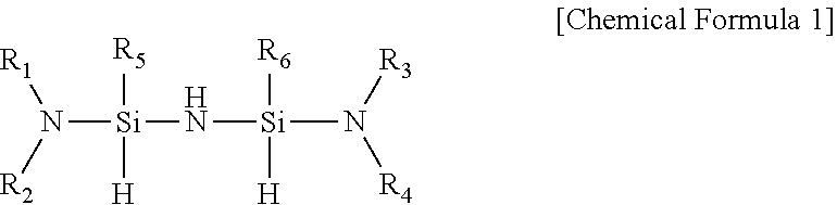
1. A composition for depositing a silicon-containing thin film, the composition comprising a silylamine compound represented by the following Chemical Formula 1: ##STR00011## in Chemical Formula 1, R.sub.1 to R.sub.4 are each independently hydrogen, C1-C7alkyl, or C2-C7alkenyl, or R.sub.1 and R.sub.2, and R.sub.3 and R.sub.4 are each independently linked to each other to form a ring; and R.sub.5 and R.sub.6 are each independently C1-C7alkyl, or C2-C7)alkenyl.
2. The composition of claim 1, wherein R.sub.5 and R.sub.6 are each independently C1-C5alkyl.
3. The composition of claim 1, wherein the silylamine compound represented by Chemical Formula 1 is represented by Chemical Formula 2 or 3: ##STR00012## in Chemical Formulas 2 and 3, R.sub.11 to R.sub.14 are each independently hydrogen, C1-C5alkyl, or C2-C5alkenyl; R.sub.5 and R.sub.6 are each independently C1-C5alkyl, or C2-C5alkenyl; and n and m are each independently an integer of 1 to 7.
4. The composition of claim 3, wherein R.sub.5 and R.sub.6 are each independently C1-C5alkyl; and n and m are each independently an integer of 1 to 4.
5. The composition of claim 1, wherein the silylamine compound is selected from the following compounds: ##STR00013##
6. A method for manufacturing a silicon-containing thin film, using a composition comprising a silylamine compound represented by the following Chemical Formula 1: ##STR00014## in Chemical Formula 1, R.sub.1 to R.sub.4 are each independently hydrogen, C1-C7alkyl, or C2-C7alkenyl, or R.sub.1 and R.sub.2, and R.sub.3 and R.sub.4 are each independently linked to each other to form a ring; and R.sub.5 and R.sub.6 are each independently C1-C7alkyl, or C2-C7)alkenyl.
7. The method of claim 6, wherein deposition is performed by an atomic layer deposition method, a chemical vapor deposition method, a metal-organic chemical vapor deposition method, a low-pressure chemical vapor deposition method, a plasma-enhanced chemical vapor deposition method, or a plasma-enhanced atomic layer deposition method.
8. The method of claim 6, wherein the silicon-containing thin film is a silicon oxide film, a silicon oxy carbide film, a silicon nitride film, a silicon oxy nitride film, a silicon carbonitride film, or a silicon carbide film.
9. The method of claim 6, comprising: a) maintaining a temperature of a substrate mounted in a chamber at 30 to 500.degree. C.; b) contacting the composition of any one of claims 1 to 5 with the substrate to adsorb the composition in the substrate; and c) injecting a reaction gas into the substrate in which the composition is adsorbed to form a silicon-containing thin film.
10. The method of claim 9, wherein the reaction gas is supplied after being activated by generating plasma with a plasma power of 50 to 1000 W.
11. The method of claim 6, wherein R.sub.5 and R.sub.6 are each independently C1-C5alkyl.
12. The method of claim 6, wherein the silylamine compound represented by Chemical Formula 1 is represented by Chemical Formula 2 or 3: ##STR00015## in Chemical Formulas 2 and 3, R.sub.11 to R.sub.14 are each independently hydrogen, C1-C5alkyl, or C2-C5alkenyl; R.sub.5 and R.sub.6 are each independently C1-C5alkyl, or C2-C5alkenyl; and n and m are each independently an integer of 1 to 7.
13. The method of claim 12, wherein R.sub.5 and R.sub.6 are each independently C1-C5alkyl; and n and m are each independently an integer of 1 to 4.
14. The method of claim 6, wherein the silylamine compound is selected from the following compounds:
Description
TECHNICAL FIELD
[0001] The present invention relates to a composition for depositing a silicon-containing thin film and a method for manufacturing a silicon-containing thin film using the same, and more particularly, to a composition for depositing a silicon-containing thin film, containing a silylamine compound as a precursor for depositing a thin film, and a method for manufacturing a silicon-containing thin film using the same.
BACKGROUND ART
[0002] A silicon-containing thin film is manufactured through various deposition processes in a semiconductor field to thereby be manufactured in various forms such as a silicon film, a silicon oxide film, a silicon nitride film, a silicon carbonitride film, and a silicon oxynitride film, and an application field of the silicon-containing thin film may be wide.
[0003] Particularly, since the silicon oxide film and the silicon nitride film have a significantly excellent barrier property and oxidation resistance, the silicon oxide film and the silicon nitride film are used as an insulating film, a diffusion barrier, a hard mask, an etch stop layer, a seed layer, a spacer, a trench isolation, an intermetallic dielectric material, and a passivation layer in manufacturing an apparatus.
[0004] Recently, a polycrystalline silicon thin film has been used in a thin film transistor (TFT), a solar cell, and the like, and an application field thereof has been gradually diversified.
[0005] As a representative technology for manufacturing a silicon-containing thin film known in the art, there are a metal-organic chemical vapor deposition (MOCVD) method for reacting a gas-type silicon precursor and a reaction gas with each other to form a film on a surface of a substrate or directly reacting the gas-type silicon precursor and the reaction gas with each other on the surface to form a film and an atomic layer deposition (ALD) method for physically or chemically adsorbing a gas-type silicon precursor and sequentially injecting a reaction gas to form a film. Various technologies for manufacturing a thin film such as a low-pressure chemical vapor deposition (LPCVD) method applying the above-mentioned method, a plasma-enhanced chemical vapor deposition (PECVD) method and a plasma-enhanced atomic layer deposition (PEALD) method capable of performing deposition at a low temperature, and the like, are applied to processes for manufacturing next-generation semiconductors and display devices to thereby be used to form a ultra-fine pattern and deposit an ultra-thin film having uniform and excellent properties at a nano-scale thickness.
[0006] Representative examples of a precursor used to form the silicon-containing thin film may include silane, silane compounds, aminosilane, and alkoxysilane compounds. Specific examples thereof may include silane chloride compounds such as dichlorosilane (SiH.sub.2Cl.sub.2) and hexachlorodisilane (Cl.sub.3SiSiCl.sub.3), trisilylamine (N(SiH.sub.3).sub.3, bis-diethylaminosilane (H.sub.2Si(N(CH.sub.2CH.sub.3).sub.2).sub.2), di-isopropylaminosilane (H.sub.3SiN(i-C.sub.3H.sub.7).sub.2), and the like. These precursors have been used in mass-production processes for manufacturing semiconductors and displays.
[0007] However, due to fineness of devices caused by ultra-high integration of the devices and an increase in aspect ratio, and diversification of materials of the devices, a technology of forming an ultra-fin thin film having a uniform and thin thickness and excellent electrical properties at a low temperature to be desired has been required. Therefore, a high-temperature process (600.degree. C. or more) using an existing silicon precursor, a step coverage, etching properties, and physical and electric properties of the thin film have become problems, such that the development of a novel more excellent silicon precursor and a method for forming a thin film have been studied.
TECHNICAL PROBLEM
[0008] An object of the present invention is to provide a composition for depositing a silicon-containing thin film, containing a silylamine compound capable of being used as a precursor of the silicon-containing thin film.
[0009] Another object of the present invention is to provide a method for manufacturing a silicon-containing thin film using the composition for depositing a silicon-containing thin film according to the present invention.
TECHNICAL SOLUTION
[0010] In one general aspect, there is provided a composition for depositing a silicon-containing thin film, containing a silylamine compound having excellent cohesive force, a high deposition rate, and excellent physical and electrical properties as a precursor for depositing a silicon-containing thin film, the silylamine compound being represented by the following Chemical Formula 1.
##STR00001##
[0011] (In Chemical Formula 1, R.sub.1 to R.sub.4 are each independently hydrogen, (C1-C7)alkyl, or (C2-C7)alkenyl, or R.sub.1 and R.sub.2, and R.sub.3 and R.sub.4 are each independently linked to each other to form a ring; and R.sub.5 and R.sub.6 are each independently (C1-C7)alkyl, or (C2-C7)alkenyl.)
[0012] Preferably, in the silylamine compound represented by Chemical Formula 1 according to the exemplary embodiment of the present invention, R.sub.5 and R.sub.6 may be each independently (C1-C5)alkyl.
[0013] Preferably, the silylamine compound represented by Chemical Formula 1 according to the exemplary embodiment of the present invention may be represented by the following Chemical Formula 2 or 3.
##STR00002##
[0014] (In Chemical Formula 2 or 3, R.sub.11 to R.sub.14 are each independently hydrogen, (C1-C5)alkyl, or (C2-C5)alkenyl; R.sub.5 and R.sub.6 are each independently (C1-C5)alkyl, or (C2-C5)alkenyl; and n and m are each independently an integer of 1 to 7.)
[0015] Preferably, in Chemical Formula 2 or 3 according to the exemplary embodiment of the present invention, R.sub.5 and R.sub.6 may be each independently (C1-C5)alkyl; and n and m may be each independently an integer of 1 to 4.
[0016] The silylamine compound represented by Chemical Formula 1 according to the exemplary embodiment of the present invention may be selected from the following compounds but is not limited thereto.
##STR00003##
[0017] In another general aspect, there is provided a method for manufacturing a silicon-containing thin film using the composition for depositing a silicon-containing thin film according to the exemplary embodiment of the present invention.
[0018] In the method for manufacturing a silicon-containing thin film, the silicon-containing thin film may be formed by an atomic layer deposition (ALD) method, a chemical vapor deposition (CVD) method, a metal-organic chemical vapor deposition (MOCVD) method, a low-pressure chemical vapor deposition (LPCVD) method, a plasma-enhanced chemical vapor deposition (PECVD) method, or a plasma-enhanced atomic layer deposition (PEALD) method, and be a silicon oxide (SiO.sub.2) film, a silicon oxy carbide (SiOC) film, a silicon nitride (SiN) film, a silicon oxy nitride (SiON) film, a silicon carbonitride (SiCN) film, or a silicon carbide (SiC) film.
[0019] More specifically, the method for manufacturing a silicon-containing thin film according to the present invention may include:
a. maintaining a temperature of a substrate mounted in a chamber at 30 to 500.degree. C.; b. contacting the composition for depositing a silicon-containing thin film according to the present invention with the substrate to adsorb the composition for depositing a silicon-containing thin film according to the present invention in the substrate; and c. injecting a reaction gas into the substrate in which the composition for depositing a silicon-containing thin film is adsorbed to form a silicon-containing thin film.
[0020] In the method for manufacturing a silicon-containing thin film, the reaction gas may be supplied after being activated by generating plasma at a plasma power of 50 to 1000 W.
ADVANTAGEOUS EFFECTS
[0021] A composition for depositing a silicon-containing thin film contains a silylamine which is a liquid at room temperate and has high volatility and excellent thermal stability as a precursor, such that a high-quality silicon-containing thin film having high purity and durability may be provided under lower plasma power and film formation temperature conditions.
[0022] Further, in a method for manufacturing a silicon-containing thin film using the composition for depositing a silicon-containing thin film according to the present invention, an excellent deposition rate and excellent stress intensity may be implemented even under a low film formation temperature condition, and in a silicon-containing thin film manufactured thereby, contents of impurities such as carbon, oxygen, and hydrogen are minimized, such that the silicon-containing thin film may have a high purity, excellent physical and electrical properties, and excellent water vapor transmission rate.
DESCRIPTION OF DRAWINGS
[0023] FIG. 1 is a view illustrating a result obtained by measuring a vapor pressure of a bis(dimethylaminomethylsilyl)amine compound prepared in Example 1.
[0024] FIG. 2 is a view illustrating a thermogravimetric analysis result of the bis(dimethylaminomethylsilyl)amine compound prepared in Example 1.
[0025] FIG. 3 is a view illustrating results obtained by performing infrared spectroscopic analysis on deposited films of silicon-containing thin films manufactured in Examples 2 to 8 and Comparative Example 2.
[0026] FIG. 4 is a view illustrating results obtained by performing infrared spectroscopic analysis on deposited films of silicon-containing thin films manufactured in Examples 9 to 15.
[0027] FIG. 5 is a result obtained by measuring a water vapor transmission rate of a silicon-containing thin film prepared in Example 6.
[0028] FIG. 6 is a result obtained by measuring a water vapor transmission rate of a silicon-containing thin film prepared in Example 11.
BEST MODE
[0029] The present invention provides a composition for depositing a silicon-containing thin film containing a silylamine compound represented by the following Chemical Formula 1, which is a liquid at room temperature and has high volatility and excellent thermal stability to thereby be used as a significantly useful precursor of forming a silicon-containing thin film, wherein the silylamine compound is represented by the following Chemical Formula 1.
##STR00004##
[0030] (In Chemical Formula 1, R.sub.1 to R.sub.4 are each independently hydrogen, (C1-C7)alkyl, or (C2-C7)alkenyl, or R.sub.1 and R.sub.2, and R.sub.3 and R.sub.4 are each independently linked to each other to form a ring; and R.sub.5 and R.sub.7 are each independently (C1-C7)alkyl, or (C2-C7)alkenyl.)
[0031] In the silylamine compound contained in the composition for depositing a silicon-containing thin film, amine has two aminosilyl functional groups as substituents, such that the silylamine compound, which is a liquid at room temperature, has high volatility. Therefore, the silylamine compound may be significantly usefully used to form the silicon-containing thin film.
[0032] More specifically, the silylamine compound according to the present invention is a compound having a silazane backbone, but necessarily has two aminosilyl functional groups
##STR00005##
and only when each silicon atom of the aminosilyl functional groups necessarily has one hydrogen atom attached thereto, the silylamine compound may have useful effects as a precursor for depositing a thin film.
[0033] Preferably, in the silylamine compound represented by Chemical Formula 1 according to the exemplary embodiment of the present invention, R5 and R6 may be each independently (C1-C5)alkyl.
[0034] Preferably, the silylamine compound represented by Chemical Formula 1 according to the exemplary embodiment of the present invention may be represented by the following Chemical Formula 2 or 3.
##STR00006##
[0035] (In Chemical Formulas 2 and 3, R.sub.11 to R.sub.14 are each independently hydrogen, (C1-C5)alkyl, or (C2-C5)alkenyl; R.sub.5 and R.sub.6 are each independently (C1-C5)alkyl, or (C2-C5)alkenyl; and n and m are each independently an integer of 1 to 7.)
[0036] In the silylamine compound according to the present invention, each silicon atom of two aminosilyl groups in the silazane backbone necessarily has one hydrogen atom attached thereto, such that the silylamine compound has a more excellent effect as the precursor for depositing a silicon-containing thin film.
[0037] Preferably, in Chemical Formula 2 or 3 according to the exemplary embodiment of the present invention, R.sub.5 and R.sub.6 may be each independently (C1-C5)alkyl or (C2-C5)alkenyl; and n and m are each independently an integer of 1 to 4. More preferably, R.sub.5 and R.sub.6 may be each independently (C1-C5)alkyl; and n and m are each independently an integer of 1 to 3.
[0038] It is more preferable that the silylamine compound represented by Chemical Formula 1 is a compound represented by the following Chemical Formula 4 in which both sides of an NH group are symmetric to each other in order to have more excellent effect as the precursor for depositing a silicon-containing thin film.
##STR00007##
[0039] (In Chemical Formula 4, R.sub.1 and R.sub.2 are each independently hydrogen, (C1-C7)alkyl, or (C2-C7)alkenyl, or R.sub.1 and R.sub.2 is linked to each other to form a ring; and R.sub.5 is (C1-C7)alkyl or (C2-C7)alkenyl.)
[0040] The silylamine compound represented by Chemical Formula 1 according to the exemplary embodiment of the present invention may be selected from the following compounds.
##STR00008##
[0041] The composition for depositing a silicon-containing thin film according to the present invention contains the silylamine compound represented by Chemical Formula 1 as the precursor for depositing a thin film, and the silylamine compound in the composition for depositing a silicon-containing thin film may be contained in a content range in which the content may be recognized by those skilled in the art in consideration of film formation conditions, a thickness, properties, or the like, of the thin film.
[0042] As used herein, the term "alkyl" means a linear, branched, and cyclic saturated and unsaturated hydrocarbons having 1 to 7 carbon atoms, preferably, 1 to 5 carbon atoms, and more preferably 1 to 3 carbon atoms, and examples thereof may include methyl, ethyl, propyl, butyl, isobutyl, pentyl, and the like.
[0043] As used herein, "halogen" refers to a halogen element, and examples thereof include fluoro, chloro, bromo, iodo.
[0044] As disclosed herein, the term "alkenyl" as a single group or a part of another group means a straight-chain, branched-chain, or cyclic hydrocarbon radical having 2 to 7 carbon atoms and one or more carbon-carbon double bonds. A more preferable alkenyl radical is a lower alkenyl radical having 2 to 5 carbon atoms. The most preferable lower alkenyl radical is a lower alkenyl radical having about 2 to 3 carbon atoms. Further, an alkenyl group may be substituted at a random usable attachment point. Examples of the alkenyl radical include ethenyl, propenyl, allyl, butenyl, and 4-methylbutenyl. The terms "alkenyl" and "lower alkenyl" include radicals having cis and trans orientations or alternatively, E and Z orientations.
[0045] As used herein, the phrase "R.sub.1 and R.sub.2, and R.sub.3 and R.sub.4 are each independently linked to each other to form a ring" includes the case in which R.sub.1 and R.sub.2 are linked to each other to form a ring but R.sub.3 and R.sub.4 do not form a ring; the case in which on the contrary, R.sub.1 and R.sub.2 do not form a ring but R.sub.3 and R.sub.4 are linked to each other to form a ring; and the case in which R.sub.1 and R.sub.2 are linked to each other to form a ring and R.sub.3 and R.sub.4 are linked to each other to form a ring, wherein the formed ring may be an alicyclic or aromatic ring containing N, and preferably, an alicyclic ring.
[0046] The silylamine compound represented by Chemical Formula 1 according to the exemplary embodiment of the present invention may be prepared by a method as long as the method may be recognized by those skilled in the art.
[0047] In addition, the present invention provides a method for manufacturing a silicon-containing thin film using the composition for depositing a silicon-containing thin film according to the present invention.
[0048] In the method for manufacturing a silicon-containing thin film according to the present invention, the composition for depositing a silicon-containing thin film according to the present invention, containing the silylamine compound represented by Chemical Formula 1 which is a liquid at room temperature and has high volatility and excellent thermal stability as the precursor is used, such that the handling may be easy, it is possible to manufacture various thin films, and it is possible to manufacture a silicon-containing thin film having a high purity at a high deposition rate even at a low temperature and a low power.
[0049] Further, a silicon-containing thin film manufactured by the method according to the present invention has excellent durability and electric properties, and resistance against hydrogen fluoride and a water vapor transmission rate are also excellent.
[0050] In the method for manufacturing a silicon-containing thin film according to the present invention, the silicon-containing thin film may be formed by any method as long as it may be recognized by those skilled in the art. However, preferably, the silicon-containing thin film may be formed by an atomic layer deposition (ALD) method, a chemical vapor deposition (CVD) method, a metal-organic chemical vapor deposition (MOCVD) method, a low-pressure chemical vapor deposition (LPCVD) method, a plasma enhanced chemical vapor deposition (PECVD) method, or a plasma enhanced atomic layer deposition (PEALD) method, but PECVD, ALD, or PEALD is more preferable in order to allow the thin film to be more easily deposited, and allow the manufactured thin film to have excellent properties.
[0051] The silicon-containing thin film according to the present invention may be a silicon oxide (SiO.sub.2) film, a silicon oxy carbide (SiOC) film, a silicon nitride (SiN) film, a silicon oxy nitride (SiON) film, a silicon carbonitride (SiCN) film, or a silicon carbide (SiC) film, and various thin films having high quality may be manufactured.
[0052] More specifically, the method for manufacturing a silicon-containing thin film according to the present invention may include:
a. maintaining a temperature of a substrate mounted in a chamber at 30 to 500.degree. C.; b. contacting the composition for depositing a silicon-containing thin film according to the present invention with the substrate to adsorb the composition for depositing a silicon-containing thin film in the substrate; and c. injecting a reaction gas into the substrate in which the composition for depositing a silicon-containing thin film is adsorbed to form a silicon-containing thin film.
[0053] More specifically, the method for manufacturing a silicon-containing thin film according to the present invention may include:
a. maintaining a temperature of a substrate mounted in a chamber at 30 to 500.degree. C.; b. contacting the composition for depositing a silicon-containing thin film with the substrate to adsorb the composition for depositing a silicon-containing thin film in the substrate; c. purging the remaining composition for depositing a silicon-containing thin film and by-products; d. injecting a reaction gas into the substrate in which the composition for depositing a silicon-containing thin film is adsorbed to form a silicon-containing thin film; and e. purging the remaining reaction gas and by-products, wherein the reaction gas in step D) may remove a ligand of the silylamine compound contained in the composition for depositing a silicon-containing thin film to form a Si--O atomic layer.
[0054] Preferably, the reaction gas according to the exemplary embodiment may be supplied after being activated by generating plasma at a plasma power of 50 to 1000 W.
[0055] In the method for manufacturing a silicon-containing thin film according to the exemplary embodiment of the present invention, deposition conditions may be adjusted depending on a structure or thermal properties of a desired thin film. Examples of the deposition condition according to the exemplary embodiment of the present invention may include an injection flow rate of the composition for depositing a silicon-containing thin film containing the silylamine compound, injection flow rates of the reaction gas and a carrier gas, pressure, RF power, the temperature of the substrate, and the like. As non-restrictive examples of the deposition conditions, the injection flow rate of the composition for depositing a silicon-containing thin film may be adjusted in a range of 10 to 1000 cc/min, the injection flow rate of the carrier gas may be adjusted in a range of 10 to 1000 cc/min, the injection flow rate of the reaction gas may be adjusted in a range of 1 to 1500 cc/min, the pressure may be adjusted in a range of 0.5 to 10 torr, the RF power may be adjusted in a range of 50 to 1000 W, preferably 400 to 800 W, and the temperature of the substrate may be adjusted in a range of 30 to 500.degree. C., preferably 50 to 200.degree. C., and more preferably 50 to 100.degree. C., but the deposition conditions are not limited thereto.
[0056] The reaction gas used in the method for manufacturing a silicon-containing thin film according to the present invention is not limited, but may be one selected from hydrogen (H.sub.2), hydrazine (N.sub.2H.sub.4), ozone (O.sub.3), oxygen (O.sub.2), nitrous oxide (N.sub.2O) ammonia (NH.sub.3), nitrogen (N.sub.2), silane (SiH.sub.4), borane (BH.sub.3), diborane (B.sub.2H.sub.6), and phosphine (PH.sub.3), or a mixed gas of one or more thereof, and the carrier gas may be one selected from nitrogen (N.sub.2), argon (Ar), and helium (He), or a mixed gas of two or more thereof.
[0057] The substrate used in the method for manufacturing a silicon-containing thin film according to the present invention may be a substrate containing one or more semiconductor materials selected from Si, Ge, SiGe, GaP, GaAs, SiC, SiGeC, InAs, and InP; a silicon-on-insulator (SOI) substrate; a quartz substrate; a glass substrate for a display; or a flexible plastic substrate made of polyimide, polyethylene terephthalate (PET), polyethylene naphthalate (PEN), polymethylmethacrylate (PMMA), polycarbonate (PC), polyethersulfone (PES), polyester, and the like, but is not limited thereto.
[0058] Further, the silicon-containing thin film may be directly formed on the substrate. Alternatively, a large number of conductive layers, dielectric layers, insulating layers, or the like, may also be formed between the substrate and the silicon-containing thin film.
[0059] Preferably, the composition for depositing a silicon-containing thin film according to the exemplary embodiment of the present invention may be used as an encapsulant of an organic light emitting diode (OLED).
[0060] The present invention will be described in detail with reference to the following Examples. The terms and words used in the present specification and claims should not be interpreted as being limited to typical meanings or dictionary definitions, but should be interpreted as having meanings and concepts relevant to the technical scope of the present invention based on the rule according to which an inventor can appropriately define the concept of the term to describe most appropriately the best method he or she knows for carrying out the present invention.
[0061] Therefore, configurations described in the embodiments and shown in the drawings of the present specification indicate only the most preferred example rather than indicating all the technical ideas of the present invention and therefore, it is to be understood that various equivalents and modifications that can replace the above configurations may be present.
[0062] Further, in all the following Examples, deposition was performed by a plasma enhanced atomic layer deposition (PEALD) method known in the art using a commercialized 200 mm single wafer shower head type ALD apparatus (CN1, Atomic Premium). In addition, deposition was performed by a plasma enhanced chemical vapor deposition (PECVD) method known in the art using a commercialized 200 mm single wafer shower head type CVD (PECVD) apparatus (CN1, Atomic Premium).
[0063] A thickness of a deposited silicon-containing thin film was measured using an ellipsometer (OPTI-PROBE 2600, THERMA-WAVE), and properties of the thin film were analyzed using infrared spectroscopy (IFS66V/S & Hyperion 3000, Bruker Optics), X-ray photoelectron spectroscopy. Further, a water vapor transmission rate (WVTR) was measured using a WVTR analyzer (MOCON, Aquatran 2), an amount of nitrogen used in measurement was 20 ml/minAir, and a WVTR measurement area was set to 50 cm.sup.2. Stress was measured using a Frontier semiconductor (FSM500TC), a measurement area was set to 160 mm, and a thickness of a silicon wafer was set to 0.725 .mu.m, such that properties of the thin film were analyzed.
Example 1
Preparation of Bis(dimethylaminomethylsilyl)amine
##STR00009##
[0065] Under an anhydrous and inert atmosphere, after putting hexamethyl disilazane (((CH.sub.3).sub.3Si).sub.2NH, 250 g (1.55 mol)) and aluminum chloride (AlCl.sub.3, 10 g (0.075 mol)) into a 2000 mL flame-dried flask, dichloro methylsilane (CH.sub.3SiHCl.sub.2, 713.19 g (6.20 mol)) was slowly added thereto while stirring the mixture and maintaining a temperature at 25.degree. C. Then, a reaction solution was slowly heated to 40.degree. C. This mixture reaction solution was stirred for 3 hours, aluminum chloride (AlCl.sub.3) was removed therefrom by filtration, and the formed chlorotrimethylsilane ((CH.sub.3).sub.3SiCl) and excessively added dichloro methylsilane (CH.sub.3SiHCl) were removed by simple distillation or distillation under reduced pressure. While stirring a recovered bis(chloromethylsilyl)amine ((CH.sub.3SiHCl).sub.2NH)) solution and maintaining a temperature at -15.degree. C., dimethylamine ((CH.sub.3).sub.2NH, 293.47 g (4.2 mol)) was slowly added thereto. After the addition was completed, the reaction solution was slowly heated to room temperature and stirred at room temperature for 6 hours. The formed white solid was removed by filtration, thereby obtaining a filtrate. A solvent was removed from this filtrate under reduced pressure, followed by distillation under reduced pressure, thereby obtaining bis(dimethylaminomethylsilyl)amine (CH.sub.3SiHN(CH.sub.3).sub.2).sub.2NH, 222.54 g (1.16 mol), yield: 75%).
[0066] .sup.1H-NMR (in C.sub.6D.sub.6):.delta. 0.12 (s, 6H, ((CH3SiHN(CH3)2)2NH), 2.47 (s, 12H, ((CH3SiHN(CH3)2)2NH), 4.43 (m, 2H, ((CH3SiHN(CH3)2)2NH), 2.0 (b, 1H, ((CH3SiHN(CH3)2)2NH).
Comparative Example 1
Preparation of Diisopropylaminosilane
##STR00010##
[0068] Diisopropylamine (280.3 g (2.77 mol)) was put into a 3 L of flame-dried Schlenk flask, and pentane was added thereto and stirred therewith. While stirring this solution and maintaining a temperature at -20.degree. C., trichlorosilane (187.60 g (1.38 mol)) was slowly added thereto, and a reaction solution was slowly heated to room temperature. This mixture reaction solution was stirred at room temperature for 4 hours, and when a white solid was formed, the white solid was removed by filtration, thereby obtaining a filtrate. A solvent was removed from this filtrate under reduced pressure, and dimethoxymethane (895.89 g (11.77 mol)) was added thereto as a solvent, and lithium hydride (LiH, 27.53 g (3.46 mol)) was slowly added thereto. After addition, the mixture was refluxed for about 6 hours while maintaining a temperature of the flask at 50.degree. C. After reflux, the flask was cooled to room temperature, and a white solid was removed by filtration, thereby obtaining a filtrate. A solvent was removed from the filtrate under reduced pressure, followed by distillation under reduced pressure, thereby obtaining diisopropylaminosilane (136.5 g, yield: 75%).
[0069] .sup.1H-NMR (in C.sub.6D.sub.6):.delta. 0.93 (d, 6H, (SiH3(N(CH(CH3)2)), 2.47 (m, 2H, (SiH3(N(CH(CH3)2)), 5.65 (s, 3H, (SiH3(NCH(CH3))2)
Example 2
Manufacturing of Silicon Oxide Thin Film by PEALD Using Bis(dimethylaminomethylsilyl)amine
[0070] Film formation was evaluated using the silylamine compound prepared in Example 1 according to the present invention as a composition for forming a silicon oxide film in a general plasma enhanced atomic layer deposition (PEALD) apparatus using a plasma enhanced atomic layer deposition (PEALD) method known in the art. As a reaction gas, nitrous oxide was used together with plasma, and nitrogen corresponding to an inert gas was used for purging. The film was formed at reaction gas and plasma time of 0.5 seconds. A specific method for depositing a silicon oxide thin film was illustrated in Table 1.
[0071] A thickness of a deposited thin film was measured using the Ellipsometer, formation of the silicon oxide thin film was analyzed using infrared spectroscopy, and a composition of the silicon oxide thin film was analyzed using X-ray photoelectron spectroscopy. Further, stress of the silicon oxide thin film was analyzed using a stress meter, and in order to measure a water vapor transmission rate (WVTR) of the thin film, the WVTR analyzer was used, thereby measuring the WVTR. Specific analysis results of the silicon oxide thin film were illustrated in Table 2, and a result obtained by analyzing the deposited film using infrared spectroscopy was illustrated in FIG. 3.
Examples 3 to 8
Manufacturing of Silicon Oxide Thin Films by PEALD Using Bis(dimethylaminomethylsilyl)amine
[0072] Film formation was evaluated using the plasma enhanced atomic layer deposition (PEALD) method known in the art in the same manner as in Example 2 except that deposition conditions were changed as illustrated in Table 1 in Example 2. Further, results obtained by analyzing the deposited films using infrared spectroscopy were illustrated in a graph of FIG. 3.
[0073] As appreciated in Examples 2 to 8 according to the present invention, a deposition rate of the silicon oxide thin film deposited so as to have a thickness of 700 .ANG. at a low temperature using the composition for depositing a silicon-containing thin film, containing bis(dimethylaminomethylsilyl)amine prepared according to the present invention was 1.87 to 1.97 .ANG./cycle, such that the deposition rate was significantly excellent.
[0074] More specifically, it may be appreciated that as compared to Comparative Example 2 in which a composition for depositing a silicon-containing thin film, containing diisopropylaminosilane as a precursor of a thin film, in Examples 2 to 8 in which the composition for depositing a silicon-containing thin film, containing a silylamine compound according to the present invention as a precursor was used, the deposition rate of the thin film was more excellent, and the water vapor transmission rate was also excellent, which may have a significant influence on increase in productivity in forming the silicon-containing thin film. As the results of analyzing the deposited thin films using the infrared spectroscopy in FIG. 3, it may be appreciated that all the thin films formed in Examples 2 to 8 were silicon oxide films. Further, the water vapor transmission rates of the silicon oxide films formed in Examples 6 were 4.5E-3 (g/[m.sup.2-day]), such that the silicon oxide films have excellent moisture proof properties. Therefore, it is judged that the silicon oxide thin films may be usefully used in entire application fields of the silicon oxide thin film, particularly, as an encapsulant of an organic light emitting diode (OLED).
[0075] A result obtained by measuring a water vapor transmission rate of a silicon-containing thin film prepared in Example 6 was illustrated in FIG. 5. The water vapor transmission rate was constantly maintained for a long period of time as illustrated in FIG. 5. Therefore, it is judged that the compound suggested in the present invention may be significantly useful in an OLED device in which an encapsulation technology of blocking oxygen and moisture is important.
Comparative Example 2
Manufacturing of Silicon Oxide Thin Film by PEALD Using Diisopropylaminosilane
[0076] Film formation was evaluated using the plasma enhanced atomic layer deposition (PEALD) method known in the art under the same deposition conditions as in Example 2 except that diisopropylaminosilane prepared in Comparative Example 1 was used, a heating temperature of the precursor was 20.degree. C., and the number of deposition was 590 cycles as illustrated in the following Table 1. The deposited thin film was analyzed by the same analysis method as in Example 2 under the same conditions as in Example 2, such that analysis results were secured. In order to perform measurement at the same thickness as those of the thin films formed in Examples 2 to 8, the number of deposition was changed. A specific method for depositing a silicon oxide thin film was illustrated in the following Table 1, and properties of the deposited thin films were illustrated in Table 2. As illustrated in Table 2, a deposition rate was 1.19 .ANG./cycle, and a water vapor transmission rate (WVTR) was 8.0E-2 (g/[m.sup.2-day]), which were lower than those of the bis(dimethylaminomethylsilyl)amine in Example 2.
TABLE-US-00001 TABLE 1 Deposition Conditions of Silicon Oxide Thin Film by PEALD Temper- Reaction Gas and Reaction ature Precursor Purge Plasma Gas Purge of Heating Injection Flow Flow RF Flow No. of Process Substrate Temperature Time Rate Time Rate Power Time Time Rate Deposition Time (.degree. C.) (.degree. C.) (sec) (sccm) (sec) (sccm) (W) (sec) (sec) (sccm) Cycle (sec) Example 2 90 70 0.1 600 0.4 800 400 0.5 0.1 300 380 418 Example 3 90 70 0.1 600 0.4 800 400 0.7 0.1 300 363 471.9 Example 4 90 70 0.1 600 0.4 800 400 0.9 0.1 300 370 555 Example 5 90 70 0.1 600 0.4 800 400 1.2 0.1 300 370 666 Example 6 90 70 0.1 600 0.4 400 400 0.9 0.1 300 370 555 Example 7 90 70 0.1 600 0.4 1400 400 0.9 0.1 300 370 555 Example 8 90 70 0.1 600 0.4 800 500 0.9 0.1 300 370 555 Comparative 90 20 0.1 600 0.4 800 400 0.5 0.1 300 590 649 Example 2
TABLE-US-00002 TABLE 2 Evaluation of Properties of Silicon Oxide Thin Film O/Si Deposition Thickness of Refractive Composition Rate Thin Film Index Ratio Stress of Film WVTR Variable (.ANG./cycle) (.ANG.) -- -- (MPa) (g/[m.sup.2-day]) Example 2 Plasma 1.87 710 1.46 1.73 -134 Unmeasured Time of 0.5 sec Example 3 Plasma 1.95 723 1.47 1.73 -193 Unmeasured Time of 0.7 sec Example 4 Plasma 1.95 721 1.47 1.73 -149 2.0E-2 Time of 0.9 sec Example 5 Plasma 1.92 711 1.48 1.73 -293 2.5E-2 Time of 1.2 sec Example 6 Reaction 1.97 731 1.48 1.72 -250 4.5E-3 Gas of 400 sccm Example 7 Reaction 1.92 711 1.47 1.73 -120 5.2E-2 Gas of 1400 sccm Example 8 RF Power of 1.95 720 1.48 1.73 -151 1.1E-2 500 W Comparative Plasma 1.19 702 1.48 1.73 -272 8.0E-2 Example 2 Time of 0.5 sec
Example 9
Manufacturing of Silicon Nitride Thin Film by PEALD Using Bis(dimethylaminomethylsilyl)amine
[0077] Film formation was evaluated using the silylamine compound prepared in Example 1 according to the present invention as a composition for forming a silicon nitride film in a general plasma enhanced atomic layer deposition (PEALD) apparatus using a plasma enhanced atomic layer deposition (PEALD) method known in the art. As a reaction gas, nitrogen and ammonia were used together with plasma as first reaction gas, and nitrogen was used as a second reaction gas. The nitrogen corresponding to an inert gas was used for purging. A specific method for depositing a silicon nitride thin film was illustrated in Table 3.
[0078] A thickness of a deposited thin film was measured using the Ellipsometer, formation of the silicon nitride thin film was analyzed using infrared spectroscopy, and a composition of the silicon nitride thin film was analyzed using X-ray photoelectron spectroscopy. Further, in order to measure a water vapor transmission rate (WVTR) of the thin film, the WVTR analyzer was used, thereby measuring the WVTR. Specific analysis results of the silicon nitride thin film were illustrated in the following Table 4, and results obtained by analyzing the deposited film using infrared spectroscopy were illustrated in FIG. 4.
Examples 10 to 15 and Comparative Example 3
Manufacturing of Silicon Nitride Thin Films by PEALD Using Bis(dimethylaminomethylsilyl)amine or Diisopropylaminosilane
[0079] Film formation was evaluated using a plasma enhanced atomic layer deposition (PEALD) method known in the art in the same manner as in Example 9 except for changing deposition conditions as in Table 3, and the deposited thin film was analyzed by the same analysis method as in Example 9 under the same conditions as in Example 9, such that analysis results were secured. A specific method for depositing a silicon nitride thin film and analysis results were illustrated in the following Tables 3 and 4. Further, the deposited films were analyzed using infrared spectroscopy, and the result was illustrated in FIG. 4. As a result, it may be appreciated that the thin film manufactured in Examples 10 to 15 were silicon nitride thin films.
[0080] Further, a result obtained by measuring a water vapor transmission rate of a silicon-containing thin film prepared in Example 11 was illustrated in FIG. 6. The water vapor transmission rate was constantly maintained for a long period of time as illustrated in FIG. 6. Therefore, it is judged that the compound suggested in the present invention may be significantly usefully used in an OLED device in which an encapsulation technology of blocking oxygen and moisture is important.
TABLE-US-00003 TABLE 3 Deposition Conditions of Silicon Nitride Thin Film by PEALD Temper- Precursor Reaction ature Heating In- Purge Reaction Gas and Plasma Gas Purge No. of of Temper- jection Flow Flow RF Flow RF Flow Depo- Process Substrate ature Time Rate Time Rate Power Time Rate Power Time Time Rate sition Time (.degree. C.) (.degree. C.) (sec) (sccm) (sec) (sccm) (W) (sec) (sccm) (W) (sec) (sec) (sccm) Cycle (sec) Example 9 90 65 0.4 6000 0.4 2000 600 0.8 6000 600 2 0.4 6000 486 2139 Example 10 90 65 0.4 6000 0.4 2000 600 1.5 6000 600 2 0.4 6000 547 2789 Example 11 90 65 0.4 6000 0.4 2000 600 1.2 6000 600 3 0.4 6000 500 2900 Example 12 90 65 0.4 6000 0.4 2000 600 0.8 6000 600 4 0.4 6000 480 3068 Example 13 90 65 0.4 6000 0.4 2000 600 1.5 6000 600 4 0.4 6000 604 4284 Example 14 90 65 0.4 6000 0.4 2000 600 1 6000 600 2 0.4 6000 493 2268 Example 15 90 65 0.4 6000 0.4 2000 800 0.6 6000 800 1.3 0.4 6000 432 1512 Comparative 90 20 0.4 6000 0.4 2000 800 0.6 6000 800 1.3 0.4 6000 697 2442 Example 3
TABLE-US-00004 TABLE 4 Evaluation of Properties of Silicon Nitride Thin Film Thickness N/Si Deposition of Thin Refractive Composition Rate Film Index Ratio WVTR Variable (.ANG./cycle) (.ANG.) -- -- (g/[m.sup.2-day]) Example Plasma Time 0.72 350 1.82 1.32 1.7E-3 9 of 0.8 sec/2 sec Example Plasma Time 0.64 350 1.87 1.22 2.2E-2 10 of 1.5 sec/2 sec Example Plasma Time 0.7 350 1.88 1.24 2.6E-4 11 of 1.2 sec/3 sec Example Plasma Time 0.73 350 1.89 1.25 1.7E-2 12 of 0.8 sec/4 sec Example Plasma Time 0.58 350 1.93 1.17 3.1E-2 13 of 1.5 sec/4 sec Example Plasma Time 0.71 350 1.83 1.26 4.1E-4 14 of 1 sec/2 sec Example Plasma 0.81 350 1.84 1.18 2.7E-3 15 Power of 800 W Plasma Time of 0.6 sec/1.3 sec Comparative Plasma 0.43 350 1.88 1.24 7.2E-3 Example Power of 3 800 W Plasma Time of 0.6 sec/1.3 sec
* * * * *


D00001

D00002

D00003

D00004

P00999
XML
uspto.report is an independent third-party trademark research tool that is not affiliated, endorsed, or sponsored by the United States Patent and Trademark Office (USPTO) or any other governmental organization. The information provided by uspto.report is based on publicly available data at the time of writing and is intended for informational purposes only.
While we strive to provide accurate and up-to-date information, we do not guarantee the accuracy, completeness, reliability, or suitability of the information displayed on this site. The use of this site is at your own risk. Any reliance you place on such information is therefore strictly at your own risk.
All official trademark data, including owner information, should be verified by visiting the official USPTO website at www.uspto.gov. This site is not intended to replace professional legal advice and should not be used as a substitute for consulting with a legal professional who is knowledgeable about trademark law.