Plasma Etching Systems And Methods With Secondary Plasma Injection
Tran; Toan Q. ; et al.
U.S. patent application number 16/704387 was filed with the patent office on 2020-04-09 for plasma etching systems and methods with secondary plasma injection. This patent application is currently assigned to Applied Materials, Inc.. The applicant listed for this patent is Applied Materials, Inc.. Invention is credited to Dmitry Lubomirsky, Soonam Park, Toan Q. Tran, Zilu Weng.
| Application Number | 20200111643 16/704387 |
| Document ID | / |
| Family ID | 58104281 |
| Filed Date | 2020-04-09 |


| United States Patent Application | 20200111643 |
| Kind Code | A1 |
| Tran; Toan Q. ; et al. | April 9, 2020 |
PLASMA ETCHING SYSTEMS AND METHODS WITH SECONDARY PLASMA INJECTION
Abstract
An apparatus for plasma processing includes a first plasma source, a first planar electrode, a gas distribution device, a plasma blocking screen and a workpiece chuck. The first plasma source produces first plasma products that pass, away from the first plasma source, through first apertures in the first planar electrode. The first plasma products continue through second apertures in the gas distribution device. The plasma blocking screen includes a third plate with fourth apertures, and faces the gas distribution device such that the first plasma products pass through the plurality of fourth apertures. The workpiece chuck faces the second side of the plasma blocking screen, defining a process chamber between the plasma blocking screen and the workpiece chuck. The fourth apertures are of a sufficiently small size to block a plasma generated in the process chamber from reaching the gas distribution device.
| Inventors: | Tran; Toan Q.; (San Jose, CA) ; Park; Soonam; (Sunnyvale, CA) ; Weng; Zilu; (San Diego, CA) ; Lubomirsky; Dmitry; (Cupertino, CA) | ||||||||||
| Applicant: |
|
||||||||||
|---|---|---|---|---|---|---|---|---|---|---|---|
| Assignee: | Applied Materials, Inc. Santa Clara CA |
||||||||||
| Family ID: | 58104281 | ||||||||||
| Appl. No.: | 16/704387 | ||||||||||
| Filed: | December 5, 2019 |
Related U.S. Patent Documents
| Application Number | Filing Date | Patent Number | ||
|---|---|---|---|---|
| 14838086 | Aug 27, 2015 | 10504700 | ||
| 16704387 | ||||
| Current U.S. Class: | 1/1 |
| Current CPC Class: | H01J 37/32715 20130101; H01J 37/32532 20130101; H01J 37/32357 20130101; H01J 37/32082 20130101; H01J 37/3244 20130101 |
| International Class: | H01J 37/32 20060101 H01J037/32 |
Claims
1. A process chamber comprising: a plasma blocking screen including a planar electrode defining a plurality of apertures therethrough, the plurality of apertures configured to receive plasma effluents, the plasma blocking screen characterized by a first side and a second side; a workpiece holder facing the second side of the plasma blocking screen, a processing region defined between the plasma blocking screen and the workpiece holder; and a lift plate surrounding the workpiece holder in a plane of an upper surface of the workpiece holder and comprising a radially inward portion, the plasma blocking screen being mechanically and electrically connected with a surface of the radially inward portion.
2. The process chamber of claim 1, wherein the lift plate is configured to lift the plasma blocking screen when the lift plate is translated in a direction away from the workpiece holder.
3. The process chamber of claim 1, further comprising a power supply configured to couple a radio frequency (RF) power across the plasma blocking screen and the workpiece holder.
4. The process chamber of claim 1, wherein the plasma blocking screen includes a rim member extending radially outward, and extending towards the radially inward portion of the lift plate from the second side of the plasma blocking screen, the rim member configured to contact the lift plate and electrically connect the plasma blocking screen with the radially inward portion of the lift plate, wherein the second side of the plasma blocking screen is disposed at a clearance height above the radially inward portion of the lift plate.
5. The process chamber of claim 4, further comprising a ceramic spacer having: a radial flange disposed on the surface of the radially inward portion of the lift plate, and a body extending radially inward from the radial flange, the body disposed between the workpiece holder and the surface of the radially inward portion of the lift plate, the body configured to reduce radial electric fields between the workpiece holder and the lift plate.
6. The process chamber of claim 5, wherein a thickness of the radial flange of the ceramic spacer is less than the clearance height, wherein the radial flange maintains surface to surface electrical contact of the rim member of the plasma blocking screen with the radially inward portion of the lift plate.
7. The process chamber of claim 5, further comprising a ceramic pumping liner disposed below the ceramic spacer and between the workpiece holder and the lift plate, the ceramic pumping liner configured to reduce radial electric fields between the workpiece holder and the lift plate.
8. The process chamber of claim 7, wherein the ceramic pumping liner is disposed between the radially inward portion of the lift plate and a base of the process chamber.
9. The process chamber of claim 7, wherein the plane of the upper surface of the workpiece holder configured to support a substrate passes through the ceramic pumping liner.
10. The process chamber of claim 1, wherein a plane extending from a surface of the lift plate facing away from the plasma blocking screen passes through the workpiece holder.
11. An apparatus for plasma processing, comprising: a planar electrode defining first apertures; a plasma source configured to generate first plasma products from one or more source gases, wherein the plasma source is configured to provide the first plasma products through the first apertures of the planar electrode; a plasma blocking screen defining second apertures , a first side of the plasma blocking screen facing the planar electrode, the plasma blocking screen characterized by a second side of the plasma blocking screen opposite the first side; a workpiece holder, wherein a processing region is defined between the second side of the plasma blocking screen and the workpiece holder; and a lift plate surrounding the workpiece holder in a plane of a first surface of the workpiece holder and forming a radially inward portion, the plasma blocking screen being mechanically and electrically connected with the radially inward portion of the lift plate.
12. The apparatus for plasma processing of claim 11, wherein the lift plate forms a recessed ledge extending to the radially inward portion and the planar electrode is supported by a radially outward wall of the recessed ledge, and wherein the lift plate is configured to lift the planar electrode and the plasma blocking screen when the lift plate is translated in a direction away from the workpiece holder.
13. The apparatus for plasma processing of claim 11, wherein the plasma blocking screen includes a rim member extending radially outward, and extending towards the radially inward portion of the lift plate from the second side of the plasma blocking screen, the rim member configured to directly contact the lift plate, wherein the second side of the plasma blocking screen is disposed at a clearance height above the radially inward portion of the lift plate.
14. The apparatus for plasma processing of claim 11, further comprising a ceramic spacer having a radial flange seated on the surface of the radially inward portion of the lift plate, and having a body extending radially inward from the radial flange, the body disposed between the workpiece holder and the surface of the radially inward portion of the lift plate.
15. The apparatus for plasma processing of claim 14, further comprising a ceramic pumping liner, disposed between the workpiece holder and the lift plate, the ceramic pumping liner configured to reduce radial electric fields between the workpiece holder and the lift plate.
16. An apparatus for plasma processing, comprising: a gas source; a first planar electrode configured to receive one or more gases from the gas source; a second planar electrode; a first power supply configured to couple a first radio frequency (RF) power across the first planar electrode and the second planar electrode, wherein the first RF power couples across the first planar electrode and the second planar electrode to generate a first plasma, from the one or more gases, between the first planar electrode and the second planar electrode, a process chamber including: a plasma blocking screen including a third planar electrode defining a plurality of apertures therethrough configured to receive the first plasma, the one or more gases, or combinations thereof, the plasma blocking screen having a first side and a second side; a workpiece holder facing the second side of the plasma blocking screen, a processing region defined between the plasma blocking screen and the workpiece holder; and a lift plate surrounding the workpiece holder in a plane of an upper surface of the workpiece holder and forming a radially inward portion, the plasma blocking screen being mechanically and electrically connected with an upward face of the radially inward portion, and a second power supply configured to couple a second radio frequency (RF) power across the plasma blocking screen and the workpiece holder, wherein the second RF power couples across the plasma blocking screen and the workpiece holder to generate a second plasma, from the first plasma, the one or more gases, or combinations thereof, between the plasma blocking screen and the workpiece holder.
17. The apparatus for plasma processing of claim 16, wherein the lift plate forms an uppermost surface disposed above the radially inward portion and the first planar electrode and the second planar electrode are supported by the uppermost surface, and wherein lifting the lift plate in a direction away from the workpiece holder lifts the first, second, and third electrodes away from the workpiece holder.
18. The apparatus for plasma processing of claim 16, wherein the second plasma generated is radially inward from the radially inward portion of the lift plate, and wherein a plane extending through the radially inward portion extends through the second plasma.
19. The apparatus for plasma processing of claim 16, wherein the plasma blocking screen further includes: a first aperture section extending from the first side of the plasma blocking screen defines an aperture axis and a first aperture minor lateral dimension perpendicular to the aperture axis, a second aperture section extending from the second side of the plasma blocking screen defines a second aperture minor lateral dimension, where it adjoins the first aperture section, wherein the second aperture minor lateral dimension is less than the first aperture minor lateral dimension, and wherein the first and second aperture sections adjoin axially to extend from the first side to the second side of the plasma blocking screen.
20. The apparatus for plasma processing of claim 19, wherein at least the second side of the plasma blocking screen, and surfaces of the second aperture section, include a ceramic coating.
Description
CROSS-REFERENCE TO RELATED APPLICATIONS
[0001] The application is a continuation of U.S. patent application Ser. No. 14/838,086, filed Aug. 27, 2015, which is hereby incorporated by reference in its entirety for all purposes.
TECHNICAL FIELD
[0002] The present disclosure relates to plasma processing systems.
BACKGROUND
[0003] In plasma processing, plasmas create ionized and/or energetically excited species for interaction with workpieces that may be, for example, semiconductor wafers. To create and/or maintain a plasma, one or more radio frequency (RF) and/or microwave generators typically generate oscillating electric and/or magnetic fields. In some wafer processing systems, a plasma is generated in the same location as one or more wafers being processed; in other cases, a plasma is generated in one location and moves to another location where the wafer(s) are processed. The plasmas produced often contain highly energetic and/or corrosive species and/or highly energetic electrons, such that the equipment that produces them sometimes degrades from contact with the energetic species and/or electrons. For example, materials that are exposed to highly energetic species and/or electrons may be etched and/or sputtered, generating etched and/or sputtered material that can move about, and can react or deposit on various surfaces.
SUMMARY
[0004] In an embodiment, an apparatus for plasma processing includes a first plasma source, a first planar electrode, a gas distribution device, a plasma blocking screen and a workpiece chuck. The first plasma source produces first plasma products. The first planar electrode includes a first plate that defines a plurality of first apertures therethrough, a first side of the first planar electrode being disposed relative to the first plasma source such that the first plasma products pass away from the first plasma source through the plurality of first apertures to a second side of the first planar electrode. The gas distribution device includes a second plate that defines a plurality of second apertures therethrough, a first side of the gas distribution device being disposed facing the second side of the first planar electrode, such that the first plasma products continue through the plurality of second apertures to a second side of the gas distribution device. The plasma blocking screen includes a third plate that defines a plurality of fourth apertures therethrough, a first side of the plasma blocking screen being disposed facing the second side of the gas distribution device such that the first plasma products pass through the plurality of fourth apertures to a second side of the plasma blocking screen. The workpiece chuck faces the second side of the plasma blocking screen, such that a process chamber is defined between the plasma blocking screen and the workpiece chuck. The fourth apertures are of a sufficiently small size to block a plasma generated in the process chamber from reaching the gas distribution device.
[0005] In an embodiment, a plasma processing chamber includes a workpiece holder and a planar electrode. The planar electrode defines parallel and opposing first and second planar surfaces, separated by a thickness, over a central region thereof. The second planar surface is disposed facing the workpiece holder. The planar electrode defines a plurality of apertures therethrough. Each of the apertures is characterized by a first aperture section and a second aperture section. The first aperture section defines an aperture axis and a first aperture minor lateral dimension perpendicular to the aperture axis, the first aperture section extending from the first planar surface through at least half of the thickness. The second aperture section defines a second aperture minor lateral dimension that is less than the first aperture minor lateral dimension, and extends from the second planar surface through less than half the thickness. The first and aperture sections adjoin axially to form a continuous one of the apertures from the first planar surface to the second planar surface.
[0006] In an embodiment, an apparatus for plasma processing includes a gas source, a first planar electrode, a second planar electrode, a first power supply, a plasma blocking screen, a workpiece chuck and a second power supply. The first planar electrode includes a first plate that defines a plurality of first apertures therethrough, a first side of the first planar electrode being disposed relative to the gas source such that gases from the gas source pass through the plurality of first apertures to a second side of the first planar electrode. The second planar electrode includes a second plate that defines a plurality of second apertures therethrough, a first side of the second planar electrode being disposed facing the second side of the first planar electrode. The first power supply couples radio frequency (RF) power across the first planar electrode and the second planar electrode. A first plasma is generated, from the gases, between the first planar electrode and the second planar electrode, and first plasma products from the first plasma pass through the plurality of second apertures to a second side of the second planar electrode. The plasma blocking screen includes a third plate that defines a plurality of third apertures therethrough, a first side of the plasma blocking screen being disposed facing the second side of the second planar electrode such that the first plasma products pass through the plurality of third apertures to a second side of the plasma blocking screen. The workpiece chuck faces the second side of the plasma blocking screen, defining a process chamber between the plasma blocking screen. The second power supply couples radio frequency (RF) power across the plasma blocking screen and the workpiece chuck, generating a second plasma, from the gases, between the plasma blocking screen and the workpiece chuck.
BRIEF DESCRIPTION OF THE DRAWINGS
[0007] The present disclosure may be understood by reference to the following detailed description taken in conjunction with the drawings briefly described below, wherein like reference numerals are used throughout the several drawings to refer to similar components. It is noted that, for purposes of illustrative clarity, certain elements in the drawings may not be drawn to scale. Specific instances of an item may be referred to by use of a numeral followed by a second numeral within parentheses (e.g., plasma blocking screens 270(1), 270(2) etc.) while numerals not followed by a dash refer to any such item (e.g., plasma blocking screens 270). In instances where multiple instances of an item are shown, only some of the instances may be labeled, for clarity of illustration.
[0008] FIG. 1 schematically illustrates major elements of a plasma processing system, according to an embodiment.
[0009] FIG. 2 schematically illustrates major elements of a plasma processing system, in a cross-sectional view, according to an embodiment.
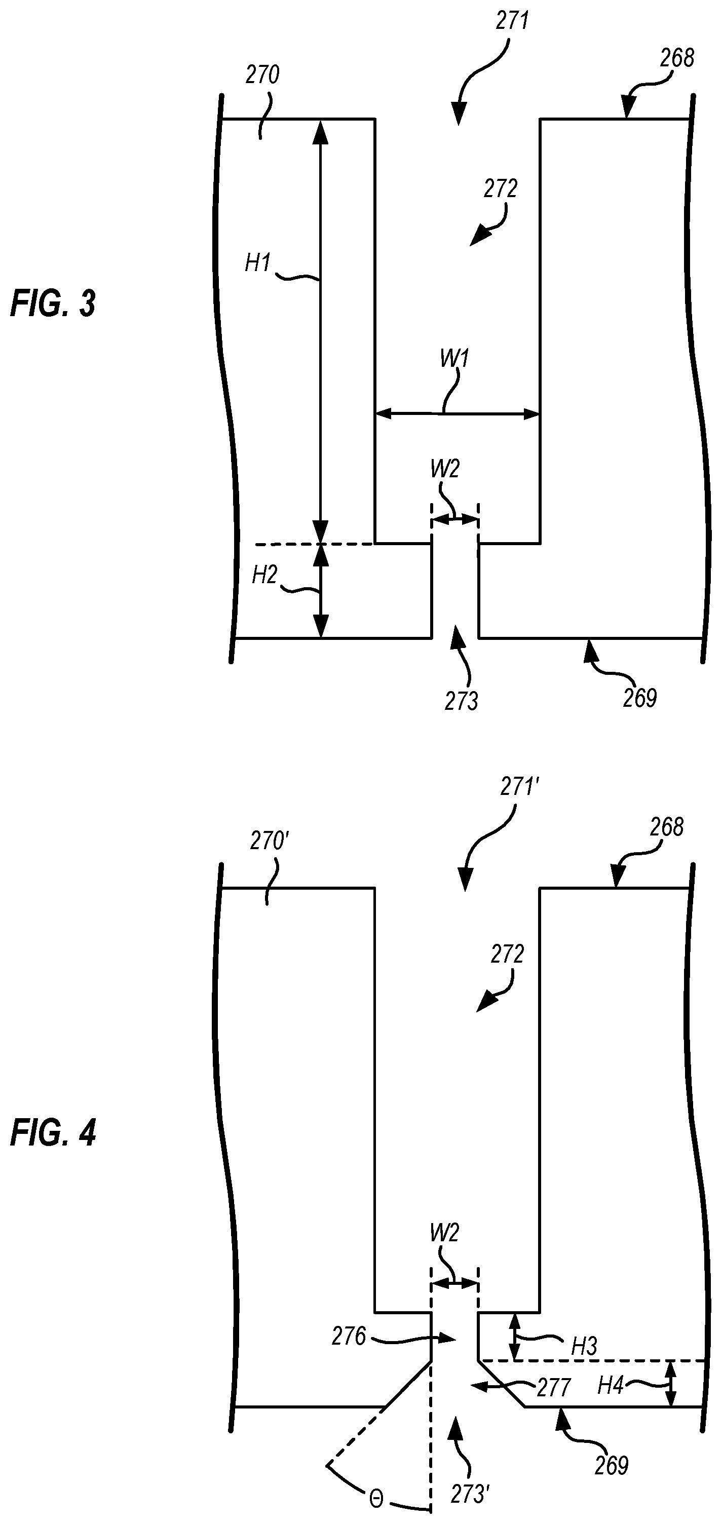
[0010] FIG. 3 illustrates a portion of a plasma blocking screen that is part of the plasma processing system of FIG. 2, according to an embodiment.
[0011] FIG. 4 illustrates a portion of another plasma blocking screen, according to an embodiment.
[0012] FIG. 5 is a graph of modeling data related to choice of a minor lateral dimension of second aperture sections of a plasma blocking screen, according to an embodiment.
[0013] FIG. 6 schematically illustrates a region noted in FIG. 2 in an enlarged view.
[0014] FIG. 7 schematically illustrates major elements of another plasma processing system, in a cross-sectional view, according to an embodiment.
[0015] Additional embodiments and features are set forth in part in the description that follows, and in part will become apparent to those skilled in the art upon examination of the specification or may be learned by the practice of the invention. The features and advantages of the invention may be realized and attained by means of the instrumentalities, combinations, and methods described in the specification.
DETAILED DESCRIPTION
[0016] FIG. 1 schematically illustrates major elements of a plasma processing system 100, according to an embodiment. System 100 is depicted as a single wafer, semiconductor wafer plasma processing system, but it will be apparent to one skilled in the art that the techniques and principles herein are applicable to plasma generation systems of any type (e.g., systems that do not necessarily process wafers or semiconductors). Processing system 100 includes a housing 110 for a wafer interface 115, a user interface 120, a plasma processing unit 130, a controller 140, one or more power supplies 150 and one or more radio frequency (RF) generators 165. Processing system 100 is supported by various utilities that may include gas(es) 155, external power 170, vacuum 160 and optionally others. Internal plumbing and electrical connections within processing system 100 are not shown, for clarity of illustration.
[0017] Processing system 100 is shown as a so-called indirect plasma processing system that generates a plasma in a first location and directs the plasma and/or plasma products (e.g., ions, molecular fragments, energized species and the like) to a second location where processing occurs. Thus, in FIG. 1, plasma processing unit 130 includes a plasma source 132 that supplies plasma and/or plasma products for a process chamber 134. Process chamber 134 includes one or more workpiece holders 135, upon which wafer interface 115 places a workpiece 50 (e.g., a semiconductor wafer, but could be a different type of workpiece) for processing. In operation, gas(es) 155 are introduced into plasma source 132, and at least one of the RF generators 165 supplies power to ignite a first plasma within plasma source 132. There may be multiple regions within plasma source 132 at which RF power is applied and plasmas are generated. Plasma and/or plasma products pass from plasma source 132 through a diffuser plate 137 to process chamber 134. Additional gases may be added to the plasma and/or plasma products in process chamber 134, RF power may also be provided within process chamber 134 to generate another plasma. Workpiece 50 is processed in process chamber 134.
[0018] Therefore, generally, plasmas may be ignited at one, two or more locations within a plasma processing system, and the techniques disclosed herein may be adapted to plasma processing systems that ignite and/or use plasmas formed at single or multiple locations. Certain electronics manufacturers may prefer systems with the flexibility of igniting and/or using plasmas in a variety of configurations, so that each system can be adapted for a corresponding variety of processing needs.
[0019] FIG. 2 schematically illustrates major elements of a plasma processing system 200, in a cross-sectional view, according to an embodiment. Plasma processing system 200 is an example of plasma processing unit 130, FIG. 1. Plasma processing system 200 includes a plasma source 210 and a process chamber 205 that may also generate a plasma, as discussed below. In the orientation of FIG. 2, a general direction of gas and/or plasma product flow is downwards, and this direction may be referred to as "downstream" herein, while an opposing direction upwards in the orientation of FIG. 2, may be referred to as "upstream." Also, significant portions of the apparatus shown in FIG. 2 may be cylindrically symmetric about a central axis 201, with associated directions being defined as a radial direction 202 and an azimuthal direction 203. This convention of directions may be used herein, although one skilled in the art will understand that many of the principles described herein are not limited to cylindrically symmetric systems.
[0020] As shown in FIG. 2, plasma source 210 may introduce gases, and/or gases that are ionized by an upstream remote plasma source, as plasma source gases 212, through an RF electrode 215. RF electrode 215 is electrically tied to a first gas diffuser 220 and a face plate 225 that serve to redirect flow of the source gases so that gas flow is uniform across plasma source 210 (uniform from left to right in the view of FIG. 2). It should be noted that all of the diffusers or screens herein may be characterized as electrodes, as any such diffusers or screens may be tied to a particular electrical potential. An insulator 230 electrically insulates RF electrode 215, including face plate 225, from a diffuser 235 that is held at electrical ground. Diffuser 235 serves as a second electrode counterfacing face plate 225 of RF electrode 215. Surfaces of face plate 225, diffuser 235 and insulator 230 define a first plasma generation cavity where a first plasma 245 may be created when plasma source gases 212 are present and RF energy is provided at face plate 225 through RF electrode 215. RF electrode 215, face plate 225 and diffuser 235 may be formed of any conductor, and in embodiments are formed of aluminum (or an aluminum alloy, such as the known "6061" alloy type). Surfaces of face plate 225 and diffuser 235 that face plasma 245 directly may be coated with ceramic layers of, for example, yttria (Y.sub.2O.sub.3) or alumina (Al.sub.2O.sub.3) for resistance to bombardment by energetic plasma products generated in plasma 245. Other surfaces of face plate 225 and diffuser 235 that are not necessarily exposed directly to plasma, but are exposed to reactive gases and/or radicals generated by plasmas, may be coated either with ceramic layers (e.g., yttria, alumina) or with a suitable passivating layer (e.g., an anodized layer, or a chemically generated alumina layer) for chemical resistance. Insulator 230 may be any insulator, and in embodiments is formed of ceramic.
[0021] Plasma products generated in plasma 245 pass through diffuser 235 that again helps to promote the uniform distribution of plasma products, and may assist in electron temperature control. Upon passing through diffuser 235, the plasma products pass through an optional gas distribution device 260 that promotes uniformity. (Certain embodiments do not include gas distribution device 260; see, e.g., FIG. 7) Optional gas distribution device 260 is also held at electrical ground. Apertures that pass completely through optional gas distribution device 260 are of a diameter at least three times a diameter of apertures within diffuser 235. Also, gas distribution device 260 includes further gas channels 250 that may be used to introduce one or more further gases 155(2) to the plasma products as they enter process chamber 205 (that is, gases 155(2) emerge only from a side of gas distribution device 260 that is distal to diffuser 235). Optional gas distribution device 260 may also be made of aluminum or aluminum alloy, and like face plate 225 and diffuser 235 discussed above, may be at least coated with a passivating layer for chemical resistance, or may be coated with a ceramic layer.
[0022] Gases 155(1), 155(2) and/or plasma products from plasma 245 enter a plenum cavity 265, then pass through a plasma blocking screen 270(1) to process chamber 205. Plasma blocking screen 270(1) may form a thickness in the range of 0.15 to 1.0 inches, and forms many small apertures that are configured to allow gases and plasma products from upstream sources pass through into process chamber 205, while substantially blocking downstream plasmas and plasma products from upstream components, as discussed in detail below. In embodiments, plasma blocking screens 270 may advantageously form at least ten apertures per square inch in a central region thereof, and in certain embodiments may form thirty or more apertures per square inch. Like optional gas distribution device 260, plasma blocking screen 270(1) is also held at electrical ground. Like face plate 225 and diffuser 235 discussed above, surfaces of plasma blocking screen 270(1) that are exposed directly to plasma are advantageously coated with ceramic (e.g., alumina or yttria) while surfaces that are not exposed directly to plasma may also be coated with ceramic, and are advantageously at least coated with a passivating layer for chemical resistance to reactive gases and activated species. All of the gases and/or plasma products, generated as described above, interact with workpiece 50 within process chamber 205, and a further plasma 275 may be generated may be generated within process chamber 205. When a plasma is desired within process chamber 205, because diffuser 235 is held at electrical ground (and, when present, optional gas distribution device 260), RF power to create plasma 275 is applied to workpiece holder 135. A DC bias may also be applied to workpiece holder 135 to steer ions generated in plasma 275 to facilitate directional (anisotropic) etching of workpiece 50, as discussed below. Workpiece holder 135 may be switchably connected with RF and/or DC bias sources, so as to generate a plasma within process chamber 205 at selected times and not at other times. Workpiece holder 135 may be connected with the same RF power supply as is used to create plasma 245 between face plate 225 and diffuser 235, or may be connected with a different RF power supply.
[0023] The use of plasma blocking screen 270(1), the ability to choose whether to generate a plasma by providing RF power and/or DC bias to workpiece holder 135, or not to generate such plasma, and other features described herein, provide application flexibility to processing system 200. For example, at a first time, processing system 200 may be operated in a mode wherein plasma is not generated within process chamber 205. At the first time, the gases and/or plasma products provided by upstream portions of processing system 200 may provide isotropic etching, and workpiece holder 135 may be held at DC ground (although a DC offset may be provided across spatial portions of workpiece holder 135, to provide electrostatic wafer chucking). At a second time, processing system 200 may be operated in a mode wherein plasma is generated within process chamber 205, and plasma products thereof may be steered by DC bias between plasma blocking screen and workpiece holder 135. At the second time, the plasma products steered by the DC bias may provide anisotropic etching, for example to remove broad surface depositions on a workpiece while leaving sidewalls, or to clear materials within deep trenches in a workpiece. Features of plasma blocking screen 270(1) are illustrated in further detail in FIGS. 3 and 4, while an enlarged view of a portion noted as A in FIG. 2 is illustrated in detail in FIG. 6.
[0024] FIG. 3 illustrates a portion of a plasma blocking screen 270, such as plasma blocking screen 270(1), FIG. 2. Plasma blocking screen 270 defines parallel and opposing planar surfaces 268 and 269, and defines a plurality of apertures 271 extending through plasma blocking screen 270, as shown in FIG. 2. First planar surface 268 and second planar surface 269 characterize a central portion of plasma blocking screen 270; however, outside the central portion, plasma blocking screen may be thicker or thinner to provide attachment points for other structures of plasma processing system 200. Apertures 271 are specialized to allow significant passage of plasma products therethrough with minimal wall effects, but to block plasma from plasma 275 from other parts of plasma processing system 200, where the plasma can damage other components. FIG. 3 illustrates features of a single aperture 271 that is characterized by a first aperture section 272 and a second aperture section 273, as shown. First aperture sections 272 may be cylindrical, which may facilitate fabrication, but may also define other shapes, for example of rectangular or hexagonal cross-section. Any such cross-section is maintained relatively constant through a vertical depth H1 of first aperture section 272 (given the orientation of plasma blocking screen 270(1) as shown in FIGS. 2 and 3) and is considered to define an aperture axis (e.g., vertical, in FIGS. 2 and 3). A minor lateral dimension of first aperture section 272 in a lateral direction (e.g., perpendicular to the aperture axis) is shown as W1. "Minor lateral dimension" herein means the largest of any lateral dimensions characterizing an aperture having vertical sides (e.g., if first aperture section 272 is cylindrical, minor lateral dimension W1 is a diameter of the cylinder, if first aperture section 272 is rectangular, minor lateral dimension W1 is the smaller of the rectangle sides, and the like). Similarly, a vertical depth of second aperture section 273 is shown as H2, while a minor lateral dimension of second aperture section 273 in a lateral direction is shown as W2. The sum of H1 and H2 is the thickness of plasma blocking screen 270 between planar surfaces 268 and 269.
[0025] Referring now to both FIG. 2 and FIG. 3, dimensions H1, W1, H2 and W2 are selected to minimize wall effects as plasma products from above (in the orientation shown in FIG. 2) pass through aperture 271, but also to block products of plasma 275 from reaching optional gas distribution device 260 (when present) and/or other upstream components of plasma processing system 200. Research has shown (see FIG. 5) that even when aperture 271 is provided with a second aperture section 273 that is very short in height, an appropriate width W2 will significantly reduce electron density within first aperture section 272 and above. The electron density can be used to estimate an extent to which any plasma product will pass through aperture 271 and affect upstream components. In embodiments herein, width W2 is less than 0.050'', while height H2 is between 0.050'' and 0.100''. For mechanical integrity, H1 is typically larger than H2, and in embodiments herein, H1 is typically 0.10'' or greater. W1 is less critical than W2, but a larger W1 reduces wall effects (e.g., recombination of ions, deactivation of activated species and the like) to maintain activity of plasma products passing through aperture 271. W1 may be, for example, 0.02'' to 0.25''.
[0026] FIG. 4 illustrates a portion of plasma blocking screen 270', which is a modified case of plasma blocking screen 270, FIG. 3. Plasma blocking screen 270' defines a plurality of apertures 271' that, like apertures 271, are specialized to allow significant passage of plasma products therethrough with minimal wall effects, but to block plasma from plasma 275 from other parts of plasma processing system 200. FIG. 4 illustrates features of a single aperture 271' that is characterized by a first aperture section 272 and a second aperture section 273', as shown. First aperture sections 272 are identical in character to the same feature illustrated in FIG. 3, and similarly, and thus may be cylindrical, which may facilitate fabrication, but first aperture sections 272 may also define other shapes, for example rectangular or hexagonal cross-sections. Second aperture section 273' defines a cylindrical upper portion 276 that adjoins first aperture section 272, and a lower portion 277 that flares outwardly from upper portion 276 toward second planar surface 269. Lower portion 277 may in fact be conical, as shown in FIG. 4, or may be simply curved outwards from the vertical. An angle .theta. from the aperture axis (e.g., vertical, in FIGS. 4) of 15 to 65 degrees may be advantageous, as discussed below. Thus, upper portion 276 may be characterized as having a diameter, and a diameter of lower portion 277 is greater where lower portion 277 adjoins planar surface 269, than the diameter of upper portion 276. Upper portion 276 and lower portion 277 adjoin axially to complete aperture 271' through plasma blocking screen 270'.
[0027] Forming apertures 271' to include conical lower portions 277 has been found advantageous for fabricating plasma blocking screen 270 with a high quality, continuous coating of alumina or yttria on surfaces (such as second planar surface 269 and side surfaces of second aperture sections 273, 273') that face active plasma. First planar surface 268 and side walls of first aperture section 272 are also, optionally, coated with alumina or yttria. As is known to those skilled in the art, certain deposition techniques such as sputtering tend to be highly directional, that is, the substance being deposited tends to travel in a straight line from a source and stick to the first thing that the substance encounters. This makes it difficult to provide films of uniform thickness and high density within narrow apertures (such as second aperture section 273, FIG. 3). Providing a conical or otherwise tapered edge section such as lower portion 277, FIG. 4, not only allows for improved deposition on the tapered edge, but also further back into upper portion 276, because each point of the interior wall of upper portion 276 "sees" a broader range of angles from which material may be deposited. For this reason, it is also appreciated that when lower portion 277 is present, certain aspect ratios of upper portion 276 (e.g., depth H3 of upper portion 276 relative to width W2 of upper portion 276, as shown in FIG. 4) and the corresponding angle .theta. thus created may be advantageous. When lower portion 277 provides relatively open access to sputtering sources, an aspect ratio within the range of 0.5 to 4.0 may advantageously provide a broad range of angles to each point on surfaces of upper portion 276.
[0028] FIG. 5 shows a graph 300 of modeling data that supports the choice of the minor lateral dimension of second aperture sections 273, 273', FIGS. 3 and 4. In graph 300, the horizontal axis models position, with conductors (e.g., workpiece holder 135 and wafer 50) assumed to be present out to about 4 centimeters, a structural void (e.g., process chamber 205 with plasma 275 therein) from about four to almost 7 centimeters (noted in graph 300 as a broken line), and plasma blocking screen 270 assumed to extend from about 7 centimeters to the end of graph 300. The vertical axis indicates modeled electron density within a plasma region between the solid conductor and the workpiece holder. The modeling assumed that a plasma was ignited with He gas at a pressure of 1 Torr and a power of 200 W. Graph 300 shows modeled electron density data for plasma blocking screen 270 having several minor lateral dimensions of second aperture section 273. Electron densities in the range of about 10.sup.2 to low 10.sup.3 are regarded as showing regions that are essentially free of plasma, that is, a number of electrons and/or other plasma products is negligibly low. Electron density is high within the plasma region, and falls off at plasma blocking screen 270. Using the notation shown in FIG. 3, all of the plasma blocking screens 270 modeled assumed H2 in the range of 0.050'' to 0.100'', W1 in the range of 0.100'' to 0.150'' and H2 in the range of 0.300'' to 0.400''. Open circle data 310 is for second aperture section 273 having W2 in the range of 0.100'' to 0.150'', solid triangle data 320 is for second aperture section 273 having W2 in the range of 0.050'' to 0.100'', and solid rectangle data 330 is for second aperture section 273 having W2 in the range of 0.020'' to 0.050''.
[0029] Data 310 and 320 show that plasma blocking screens 270 having second apertures with the respective W2 noted will decrease electron density transmitted to an adjacent region (e.g., a region extending to the right hand side of graph 300, or above plasma blocking screen 270(1) in FIG. 2), but will not effectively block it. Data 330 shows that a plasma blocking screen 270 having W2 in the range of 0.020'' to 0.050'' will block plasma almost completely from the adjacent upstream region. Although effective at blocking active plasma from the upstream region, plasma blocking screen 270 does not block plasma products from upstream plasmas, and/or gases, from passing in the downstream direction.
[0030] FIG. 6 schematically illustrates region A noted in FIG. 2. As in FIG. 2, a workpiece 50 is shown on a workpiece holder 135 within process chamber 205. Gases 155 and/or previously formed plasma products flow through plasma blocking screen 270(1) into process chamber 205, where a further plasma 275 is formed. As noted above, plasma blocking screen 270(1) is held at electrical ground. RF energy, and a DC bias, are applied to workpiece holder 135 to provide energy for plasma 275. Due to the presence of both reactive species and ion bombardment sources within process chamber 205, interior surfaces of process chamber 205 are provided with materials (generally, but not limited to, ceramics) capable of resisting attack from such sources. Materials may also be chosen to manage electric field distributions, both in a DC sense and an AC sense, to maximize RF power delivery into plasma 275. For example, workpiece holder 135 may be coated with alumina or aluminum nitride, and plasma blocking screen 270(1) may be coated with alumina or yttria. An optional ceramic spacer 350 and/or an optional ceramic pumping liner 370 may be used to reduce lateral electric fields at the edge of workpiece holder 135. Ceramic spacer 350 and ceramic pumping liner 370 are ring shaped such that they extend about a periphery of process chamber 205, but not across the central region of process chamber 205, and are advantageously fabricated from low loss tangent materials such as high purity alumina, silicon nitride and/or silicon carbide. Materials having loss tangents within the range of 0.1 to 0.0001 provide useful results, while materials having loss tangents within the range of 0.005 to 0.001 represent a range of high performance at reasonable cost. Portions of both plasma blocking screen 270(1) and ceramic spacer 350 are disposed atop a portion of a grounded lift plate 390, as shown, and obtain mechanical support therefrom. Lift plate 390 is mechanically connected with plasma blocking screen 270(1), ceramic spacer 350 and other overlying structures so as to enable lifting of all such structures from the vicinity of workpiece holder 135 for assembly and/or maintenance purposes. Plasma blocking screen 270(1) is electrically grounded through contact with lift plate 390. A thickness of ceramic spacer 350 is controlled to leave a gap 360 between plasma blocking screen 270(1) and ceramic spacer 350, to ensure that ceramic spacer 350 does not interrupt continuous contact of plasma blocking screen 270(1) with lift plate 390 in the azimuthal direction, about a periphery of process chamber 205.
[0031] Forming ceramic spacer 350 and ceramic pumping liner 370 of low loss tangent dielectric materials is comparatively expensive (as compared to, for example, fabricating such items from aluminum with a ceramic coating) but reduces electric field effects at the edges of workpiece holder 135, and reduces reflected RF power when plasma 275 is generated within process chamber 205. Substituting ceramic spacer 350 and ceramic pumping liner 370 also reduces ion bombardment related contamination as compared with equivalent aluminum parts used in the same locations. Use of ceramic spacer 350 and ceramic pumping liner 370 thus promotes plasma and process stability, and reduces contamination. Electric fields are schematically illustrated using dotted arrows in FIG. 6; the primary electric field is between workpiece holder 135/workpiece 50 and plasma blocking screen 270(1). It is advantageous for the electric fields between workpiece holder 135/workpiece 50 and plasma blocking screen 270(1) be strong and uniform in direction, since the electric fields steer ions involved with anisotropic etching. That is, to clear material at the bottoms of vertical trenches, the electric fields steering the ions need to be correspondingly vertical. Weaker fields exist between workpiece holder 135 and grounded lift plate 390, through ceramic spacer 350 and ceramic pumping liner 370. These electric fields are weakened by the dielectric materials of ceramic spacer 350 and ceramic pumping liner 370 being interposed between workpiece holder 135 and lift plate 390. Weakening the sideways electric fields at edges of workpiece holder 135 has two benefits; (1) electric field directionality, and thus etch directionality, is maintained out to edges of workpiece 50, and (2) the weaker fields generate less sputtering damage than higher fields.
[0032] FIG. 7 schematically illustrates major elements of a plasma processing system 400, in a cross-sectional view, according to an embodiment. Plasma processing system 400 is an example of plasma processing unit 130, FIG. 1. Like plasma processing system 200, FIG. 2, plasma processing system 400 enables creation of a plasma 275 adjacent to workpiece 50. Plasma processing system 400 includes many components identical in structure and function to those found in plasma processing system 200, FIG. 2, but lacks optional gas distribution device 260 shown in plasma processing system 200. Also, plasma processing system 400 includes a plasma blocking screen 270(2) configured differently from the equivalent item shown in FIG. 2, and an insulator 280 between diffuser 235 and plasma blocking screen 270(2).
[0033] Similarly to plasma processing system 200, an insulator 230 electrically insulates RF electrode 215, including face plate 225, from a diffuser 235 that is held at electrical ground. Diffuser 235 serves as a second electrode counterfacing face plate 225 of RF electrode 215. Surfaces of face plate 225, diffuser 235 and insulator 230 define a first plasma generation cavity where a first plasma 245 may be created when plasma source gases 212 are present and RF energy is provided at face plate 225 through RF electrode 215. Plasma blocking screen 270(2) is also held at electrical ground, but insulator 280 allows plasma blocking screen 270(2) to be isolated from diffuser 235, providing an independent RF ground return path. Apertures within plasma blocking screen 270(2) are configured like those of plasma blocking screen 270(1), that is, they form shapes like those illustrated in FIGS. 3 and 4, with similar dimensions, so that upstream plasma products may pass through, but active plasma 275 is blocked from diffuser 235 and other upstream components.
[0034] Embodiments herein may be rearranged and may form a variety of shapes. For example, many components shown in FIG. 2 and FIG. 7, such as RF electrode 215, diffusers 220 and 235, gas distribution device 260, face plate 225, insulator 230, plasma blocking screens 270 and others may be substantially radially symmetric about a central axis, for processing a circular semiconductor wafer as workpiece 50. However, such features may be of any shape that is consistent with use as a plasma source. An exact number and placement of features for introducing and distributing gases and/or plasma products, such as diffusers, face plates and the like, may also vary. Moreover, in a similar manner to gas distribution device 260 including gas channels 250 to add gas 155(2) to plasma products from plasma 245 as they enter process chamber 205, other components of plasma processing system 200 may be configured to add or mix gases 155 with other gases and/or plasma products as they pass through the system to process chamber 205. As also suggested by FIG. 2, FIG. 6 and FIG. 7, many system components will form perforate planar shapes within central regions of a plasma processing unit so as to provide uniform process conditions to a planar workpiece, but may form different shapes such as flanges, thickness changes, solid imperforate surfaces, and the like at edges of the plasma processing unit for structural purposes. Extents of the central regions may vary, in embodiments, to accommodate different workpiece sizes, especially but not limited to, diameters of wafers as workpieces. When the workpiece is a wafer, the central region will generally encompass a central region that extends at least to one-half of a radius of each such system component.
[0035] Specific details are given in the above description to provide a thorough understanding of the embodiments. However, it is understood that the embodiments may be practiced without these specific details. For example, well-known processes, structures, and techniques may be shown without unnecessary detail in order to avoid obscuring the embodiments. While the principles of the disclosure have been described above in connection with specific apparatuses and methods, it is to be clearly understood that this description is made only by way of example and not as limitation on the scope of the disclosure.
[0036] It is appreciated that the arrangements shown are exemplary only; other embodiments may differ greatly in configuration, including how source gases are introduced, how electrodes and insulators are arranged, how plasma and/or plasma products are handled after generation, and how grooves are formed in insulators. It is contemplated that the techniques and apparatus disclosed herein are applicable to these and other arrangements wherein conductive material builds up during use and thereby creates leakage and/or discharge paths.
[0037] As used herein and in the appended claims, the singular forms "a", "an", and "the" include plural referents unless the context clearly dictates otherwise. Thus, for example, reference to "a process" includes a plurality of such processes and reference to "the electrode" includes reference to one or more electrodes and equivalents thereof known to those skilled in the art, and so forth. Also, the words "comprise," "comprising," "include," "including," and "includes" when used in this specification and in the following claims are intended to specify the presence of stated features, integers, components, or steps, but they do not preclude the presence or addition of one or more other features, integers, components, steps, acts, or groups.
* * * * *
D00000
D00001
D00002
D00003
D00004
D00005
D00006
XML
uspto.report is an independent third-party trademark research tool that is not affiliated, endorsed, or sponsored by the United States Patent and Trademark Office (USPTO) or any other governmental organization. The information provided by uspto.report is based on publicly available data at the time of writing and is intended for informational purposes only.
While we strive to provide accurate and up-to-date information, we do not guarantee the accuracy, completeness, reliability, or suitability of the information displayed on this site. The use of this site is at your own risk. Any reliance you place on such information is therefore strictly at your own risk.
All official trademark data, including owner information, should be verified by visiting the official USPTO website at www.uspto.gov. This site is not intended to replace professional legal advice and should not be used as a substitute for consulting with a legal professional who is knowledgeable about trademark law.