Gas Distribution Device For A Wafer Processing Apparatus
Raisanen; Petri ; et al.
U.S. patent application number 15/998775 was filed with the patent office on 2020-02-20 for gas distribution device for a wafer processing apparatus. The applicant listed for this patent is ASM IP Holding B.V.. Invention is credited to Ward Johnson, Petri Raisanen.
| Application Number | 20200056282 15/998775 |
| Document ID | / |
| Family ID | 69523107 |
| Filed Date | 2020-02-20 |


| United States Patent Application | 20200056282 |
| Kind Code | A1 |
| Raisanen; Petri ; et al. | February 20, 2020 |
GAS DISTRIBUTION DEVICE FOR A WAFER PROCESSING APPARATUS
Abstract
A reaction system is disclosed that may be used to prevent formation of contaminants. The reaction system includes a showerhead that may be configured with a gated nanochannel grid to prevent particular gaseous precursors from passing through depending on whether a voltage is applied. The gated nanochannel grid may allow for both polar and non-polar molecules to pass, or may be configured to allow just non-polar or just polar molecules to pass.
| Inventors: | Raisanen; Petri; (Gilbert, AZ) ; Johnson; Ward; (Gilbert, AZ) | ||||||||||
| Applicant: |
|
||||||||||
|---|---|---|---|---|---|---|---|---|---|---|---|
| Family ID: | 69523107 | ||||||||||
| Appl. No.: | 15/998775 | ||||||||||
| Filed: | August 16, 2018 |
| Current U.S. Class: | 1/1 |
| Current CPC Class: | C23C 16/45544 20130101; C23C 16/45553 20130101; C23C 16/45565 20130101; C23C 16/4402 20130101; H01L 21/67017 20130101; C23C 16/52 20130101 |
| International Class: | C23C 16/44 20060101 C23C016/44; H01L 21/67 20060101 H01L021/67; C23C 16/455 20060101 C23C016/455; C23C 16/52 20060101 C23C016/52 |
Claims
1. A gas distribution device configured to distribute a gaseous precursor over a semiconductor substrate comprising: a top plate with at least a first top aperture through which a first gaseous precursor flows; a first plenum disposed below the top plate; a first gated nanochannel grid; a first voltage source configured to apply a voltage to the first gated nanochannel grid; an electrical isolation plate; a bottom plate; and a plurality of first bottom apertures, wherein the plurality of first bottom apertures are formed in the electrical isolation plate and the bottom plate, wherein the voltage applied to the first gated nanochannel grid determines whether the first gated nanochannel grid permits the first gaseous precursor to pass through the plurality of first bottom apertures.
2. The gas distribution device of claim 1, further comprising: a second plenum through which a second gaseous precursor flows; a second gated nanochannel grid; a second voltage source configured to apply a voltage to the second gated nanochannel grid; and a plurality of second bottom apertures through which the second gaseous precursor flows, wherein the voltage applied to the second gated nanochannel grid determines whether the second gated nanochannel grid permits the second gaseous precursor to pass through the plurality of second bottom apertures.
3. The gas distribution device of claim 1, wherein the first gated nanochannel grid always permits a non-polar gas to pass through to the plurality of first bottom apertures.
4. The gas distribution device of claim 2, wherein the second gated nanochannel grid always permits a non-polar gas to pass through to the plurality of second bottom apertures.
5. The gas distribution device of claim 1, wherein the first voltage applied to the first gated nanochannel grid determines whether a non-polar gas passes through to the plurality of first bottom apertures.
6. The gas distribution device of claim 2, wherein the second voltage applied to the second gated nanochannel grid determines whether a non-polar gas passes through to the plurality of second bottom apertures.
7. The gas distribution device of claim 1, wherein the first gated nanochannel grid comprises at least one of: mesoporous alumina, mesoporous silica, or carbon nanotubes.
8. The gas distribution device of claim 2, wherein the second gated nanochannel grid comprises at least one of: mesoporous alumina, mesoporous silica, or carbon nanotubes.
9. An apparatus for depositing a film on a semiconductor wafer comprising: a reaction chamber; a first gas source configured to provide a first gaseous precursor; a wafer holder configured to hold a semiconductor wafer; and a gas distribution device configured to distribute the first gaseous precursor over the semiconductor wafer, the gas distribution device comprising: a top plate with at least a first top aperture through which the first gaseous precursor flows; a first plenum disposed below the top plate; a first gated nanochannel grid; a first voltage source configured to apply a voltage to the first gated nanochannel grid; an electrical isolation plate; a bottom plate; and a plurality of first bottom apertures, wherein the plurality of first bottom apertures are formed in the electrical isolation plate and the bottom plate, wherein the voltage applied to the first gated nanochannel grid determines whether the first gated nanochannel grid permits the first gaseous precursor to pass through the plurality of first bottom apertures.
10. The apparatus of claim 1, wherein the gas distribution device further comprises: a second plenum through which a second gaseous precursor flows; a second gated nanochannel grid; a second voltage source configured to apply a voltage to the second gated nanochannel grid; and a plurality of second bottom apertures through which the second gaseous precursor flows, wherein the voltage applied to the second gated nanochannel grid determines whether the second gated nanochannel grid permits the second gaseous precursor to pass through the plurality of second bottom apertures.
11. The apparatus of claim 9, wherein the first gated nanochannel grid always permits a non-polar gas to pass through to the plurality of first bottom apertures.
12. The apparatus of claim 10, wherein the second gated nanochannel grid always permits a non-polar gas to pass through to the plurality of second bottom apertures.
13. The apparatus of claim 9, wherein the first voltage applied to the first gated nanochannel grid determines whether a non-polar gas passes through to the plurality of first bottom apertures.
14. The apparatus of claim 10, wherein the second voltage applied to the second gated nanochannel grid determines whether a non-polar gas passes through to the plurality of second bottom apertures.
15. The apparatus of claim 9, wherein the first gated nanochannel grid comprises at least one of: mesoporous alumina, mesoporous silica, or carbon nanotubes.
16. The apparatus of claim 10, wherein the second gated nanochannel grid comprises at least one of: mesoporous alumina, mesoporous silica, or carbon nanotubes.
Description
FIELD OF INVENTION
[0001] The present disclosure generally relates to an apparatus for processing semiconductor wafers. More particularly, the disclosure relates to a gas distribution device within the apparatus capable for flowing two or more chemical precursors over the semiconductor wafers.
BACKGROUND OF THE DISCLOSURE
[0002] In film deposition systems, gases are passed over semiconductor wafers, whereby the gases may react with other gaseous precursors in order to form a particular film. These systems may include a distribution system to evenly flow the gases over the semiconductor wafers. These distribution systems may be also known as a showerhead system.
[0003] The showerhead system may be a dual flow showerhead system, in which multiple gaseous precursors pass through and are distributed onto the semiconductor wafer. The dual flow showerhead system may include multiple plenums that separate the different gaseous precursors. It is in these plenums that particular gases may stick and remain, despite the passage of purge gases through these plenums for cleaning out the remaining sticking gases. If different gas precursors share a plenum, there may be the potential for overlapping pulses of gases, as well as unwanted chemical vapor deposition (CVD) growth at the wafer level. In addition, a shared plenum may result in deposition within the showerhead, leading to formation of particles that may adversely affect the semiconductor wafer. Other potential issues include a reduction in the chamber lifetime due to the CVD growth or particle formation.
[0004] As a result, a showerhead system that avoids the issues of overlapping pulses and unwanted CVD growth by addressing gaseous precursors that may stick to the plenum or other parts of the showerhead system is desired.
SUMMARY OF THE DISCLOSURE
[0005] This summary is provided to introduce a selection of concepts in a simplified form. These concepts are described in further detail in the detailed description of example embodiments of the disclosure below. This summary is not intended to identify key features or essential features of the claimed subject matter, nor is it intended to be used to limit the scope of the claimed subject matter.
[0006] In accordance with at least one embodiment of the invention, a gas distribution device comprises: a top plate with at least a first top aperture through which a first gaseous precursor flows; a first plenum disposed below the top plate; a first gated nanochannel grid; a first voltage source configured to apply a voltage to the first gated nanochannel grid; an electrical isolation plate; a bottom plate; and a plurality of first bottom apertures, wherein the plurality of first bottom apertures are formed in the electrical isolation plate and the bottom plate; wherein the voltage applied to the first gated nanochannel grid determines whether the first gated nanochannel grid permits the first gaseous precursor to pass through the plurality of first bottom apertures.
[0007] In accordance with at least one embodiment of the invention, an apparatus for depositing a film on a semiconductor wafer comprises: a reaction chamber; a first gas source configured to provide a first gaseous precursor; a wafer holder configured to hold a semiconductor wafer; and a gas distribution device configured to distribute the first gaseous precursor over the semiconductor wafer, the gas distribution device comprising: a top plate with at least a first top aperture through which the first gaseous precursor flows; a first plenum disposed below the top plate; a first gated nanochannel grid; a first voltage source configured to apply a voltage to the first gated nanochannel grid; an electrical isolation plate; a bottom plate; and a plurality of first bottom apertures, wherein the plurality of first bottom apertures are formed in the electrical isolation plate and the bottom plate; wherein the voltage applied to the first gated nanochannel grid determines whether the first gated nanochannel grid permits the first gaseous precursor to pass through the plurality of first bottom apertures.
BRIEF DESCRIPTION OF THE DRAWING FIGURES
[0008] These and other features, aspects, and advantages of the invention disclosed herein are described below with reference to the drawings of certain embodiments, which are intended to illustrate and not to limit the invention.
[0009] FIG. 1 is a cross-sectional illustration of a semiconductor wafer processing system with a single plenum showerhead in accordance with at least one embodiment of the invention.
[0010] FIG. 2 is a cross-sectional zoomed illustration of a gas distribution device or showerhead with a single plenum in accordance with at least one embodiment of the invention.
[0011] FIGS. 3A and 3B are illustrations showing operation of a portion of the gas distribution device or showerhead in accordance with at least one embodiment of the invention.
[0012] FIG. 4 is a cross-sectional zoomed illustration of a gas distribution device or showerhead with a dual plenum in accordance with at least one embodiment of the invention.
[0013] It will be appreciated that elements in the figures are illustrated for simplicity and clarity and have not necessarily been drawn to scale. For example, the dimensions of some of the elements in the figures may be exaggerated relative to other elements to help improve understanding of illustrated embodiments of the present disclosure.
DETAILED DESCRIPTION OF EXEMPLARY EMBODIMENTS
[0014] Although certain embodiments and examples are disclosed below, it will be understood by those in the art that the invention extends beyond the specifically disclosed embodiments and/or uses of the invention and obvious modifications and equivalents thereof. Thus, it is intended that the scope of the invention disclosed should not be limited by the particular disclosed embodiments described below.
[0015] The illustrations presented herein are not meant to be actual views of any particular material, structure, or device, but are merely idealized representations that are used to describe embodiments of the disclosure.
[0016] As used herein, the term "wafer" may refer to any underlying material or materials that may be used, or upon which, a device, a circuit or a film may be formed.
[0017] As used herein, the term "atomic layer deposition" (ALD) may refer to a vapor deposition process in which deposition cycles, preferably a plurality of consecutive deposition cycles, are conducted in a process chamber. Typically, during each cycle the precursor is chemisorbed to a deposition surface (e.g., a substrate surface or a previously deposited underlying surface such as material from a previous ALD cycle), forming a monolayer or sub-monolayer that does not readily react with additional precursor (i.e., a self-limiting reaction). Thereafter, if necessary, a reactant (e.g., another precursor or reaction gas) may subsequently be introduced into the process chamber for use in converting the chemisorbed precursor to the desired material on the deposition surface. Typically, this reactant is capable of further reaction with the precursor. Further, purging steps may also be utilized during each cycle to remove excess precursor from the process chamber and/or remove excess reactant and/or reaction byproducts from the process chamber after conversion of the chemisorbed precursor. Further, the term "atomic layer deposition," as used herein, is also meant to include processes designated by related terms such as, "chemical vapor atomic layer deposition," "atomic layer epitaxy" (ALE), molecular beam epitaxy (MBE), gas source MBE, or organometallic MBE, and chemical beam epitaxy when performed with alternating pulses of precursor composition(s), reactive gas, and purge (e.g., inert carrier) gas.
[0018] As used herein, the term "chemical vapor deposition" (CVD) may refer to any process wherein a substrate is exposed to one or more volatile precursors, which may react and/or decompose on a substrate surface to produce a desired deposition.
[0019] As used herein, the term "contaminant" may refer to any unwanted material disposed within the reaction chamber that may affect the purity of a wafer disposed in the reaction chamber. The term "contaminant" may refer to, but is not limited to, unwanted deposits, metal and non-metal particles, impurities, and waste products, disposed within the reaction chamber.
[0020] In ALD processes, it may be paramount to keep gaseous precursors separated so that a reaction between at least two gaseous precursors can take place as close to the wafer surface as possible. Should the at least two gaseous precursors react in a CVD reaction further away from the wafer surface, this may result in the formation of contaminants. These contaminants can adversely affect the film formed on the wafer.
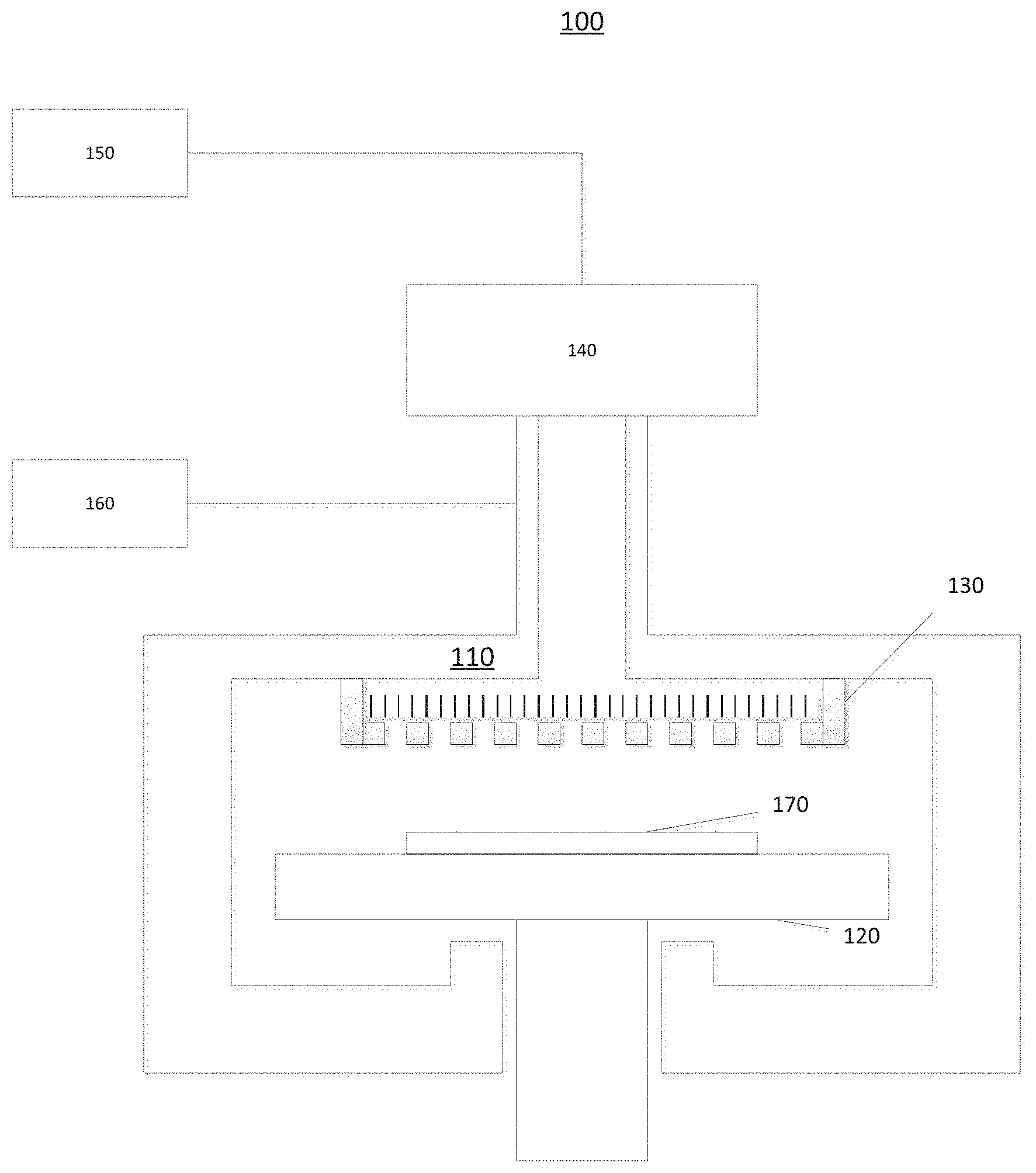
[0021] FIG. 1 illustrates a reaction system 100 in accordance with at least one embodiment of the invention. The reaction system 100 may comprise a reaction chamber 110; a susceptor 120; a showerhead 130; an optional remote plasma unit 140; a first gas source 150; and a second gas source 160. The susceptor 120 may be configured to hold a semiconductor wafer 170.
[0022] The first gas source 150 provides a first gaseous precursor to the semiconductor wafer 170, while the second gas source 160 provides a second gaseous precursor to the semiconductor wafer 170. At the semiconductor wafer 170, the first gaseous precursor and the second gaseous precursor react in order to form a film on the semiconductor wafer 170. The reaction system 100 may also include a purge gas source (not illustrated) to remove any excess of the first gaseous precursor or the second gaseous precursor from the reaction system 100.
[0023] The showerhead 130 may allow for even distribution of the first gaseous precursor (from the first gas source 150) and the second gaseous precursor (from the second gas source 160) across the semiconductor wafer 170. FIG. 2 illustrates a detailed view of the showerhead 130. The showerhead 130 may comprise a top plate 200; a gated nanochannel grid 210; an electrical isolation plate 220; a bottom plate 230; and a voltage source 240. The top plate 200 may include a top aperture 250. The electrical isolation plate 220 and the bottom plate 230 may have a plurality of bottom apertures 260. Through the top aperture 250 and the bottom apertures 260, the first gaseous precursor and the second gaseous precursor can pass to get to the semiconductor wafer 170.
[0024] The voltage source 240 may apply a voltage to the gated nanochannel grid 210. While a voltage source is contemplated, the gated nanochannel grid 210 may be controlled by any method that can change an energy state, such as a magnetic field, for example. In addition, the gated nanochannel grid 210 may comprise, for example, mesoporous alumina, mesoporous silica, or carbon nanotubes. Depending on the status of the voltage source 240 (as to whether a voltage is applied or not), the gated nanochannel grid 210 may be permissive or not as to whether it allows particular molecules to pass. An example of the operation of a gated nanochannel grid 210 is described in Guan et al., "Voltage gated ion and molecule transport in engineered nanochannels: theory, fabrication and applications," Nanotechnology 25 (2014) 122001, which is incorporated herein by reference.
[0025] FIGS. 3A and 3B illustrate a close-up operation of a single aperture of the showerhead 130. In FIG. 3A, the voltage source 240 does not apply a voltage to the gated nanochannel grid 210. As a result, the gated nanochannel grid 210 remains open and allows both a plurality of nitrogen molecules 270 and a plurality of water molecules 280 to pass through the bottom aperture 260 to the semiconductor wafer 170.
[0026] FIG. 3B illustrates the situation where the voltage source 240 does apply a voltage to the gated nanochannel grid 210. In this case, the gated nanochannel grid 210 closes up and only allows a plurality of nitrogen molecules 270 to pass through. In other words, the gated nanochannel grid 210 can selectively allow non-polar molecules (like the nitrogen molecules) to pass through to the bottom aperture 260 and the semiconductor wafer 170. The gated nanochannel grid 210 also prevents polar molecules (like the plurality of water molecules 280) from passing through. The gated nanochannel grid 210 may also be configured to allow polar molecules to pass, but not non-polar molecules.
[0027] The gated nanochannel grid 210 allows for an immediate barrier to be formed, which may be beneficial in at least providing a clean separation of gaseous precursors that reach the semiconductor wafer 170. This would be beneficial for ALD processes, which require separation of the gaseous precursors to prevent any CVD reactions from occurring to form contaminants. The reduction of CVD reactions may also improve chamber life, and reduce the cost of ownership. Furthermore, the reduction of contaminants created by CVD reactions would result in improved film uniformity, improved film quality, or defect reductions.
[0028] A situation may arise in which it would be necessary to separate gaseous precursors until the gaseous precursors reach inside of the reaction chamber. FIG. 4 illustrates a gas distribution device or showerhead 130 capable of such separation. The showerhead 130 may comprise a top plate 300; a first gated nanochannel grid 310; an electrical isolation plate 320; a bottom plate 330; and a first voltage source 340. The top plate 300 may include a top aperture 350. The electrical isolation plate 320 and the bottom plate 330 may have a plurality of first bottom apertures 360. Through the top aperture 350 and the first bottom apertures 360, the first gaseous precursor can pass to get to the semiconductor wafer 170.
[0029] The showerhead 130 also comprises a second gaseous precursor plenum 370; a second gated nanochannel grid 380; a plurality of second bottom apertures 390; and a second voltage source 400. The first voltage source 340 and the second voltage source 400 operate the first gated nanochannel grid 310 and the second gated nanochannel grid 380 in a manner described above.
[0030] The second gaseous precursor can enter into the second gaseous precursor plenum 370 via a channel (not illustrated) within the showerhead 130 from a second gas source (also not illustrated). The operation of the second voltage source 400 and the second gated nanochannel grid 380 may determine whether the second gaseous precursor remains in the second gaseous precursor plenum 370 or passes down through the plurality of second bottom apertures 390 and onto the semiconductor wafer 170.
[0031] The particular implementations shown and described are illustrative of the invention and its best mode and are not intended to otherwise limit the scope of the aspects and implementations in any way. Indeed, for the sake of brevity, conventional manufacturing, connection, preparation, and other functional aspects of the system may not be described in detail. Furthermore, the connecting lines shown in the various figures are intended to represent exemplary functional relationships and/or physical couplings between the various elements. Many alternative or additional functional relationship or physical connections may be present in the practical system, and/or may be absent in some embodiments.
[0032] It is to be understood that the configurations and/or approaches described herein are exemplary in nature, and that these specific embodiments or examples are not to be considered in a limiting sense, because numerous variations are possible. The specific routines or methods described herein may represent one or more of any number of processing strategies. Thus, the various acts illustrated may be performed in the sequence illustrated, in other sequences, or omitted in some cases.
[0033] The subject matter of the present disclosure includes all novel and nonobvious combinations and subcombinations of the various processes, systems, and configurations, and other features, functions, acts, and/or properties disclosed herein, as well as any and all equivalents thereof.
* * * * *
D00000
D00001
D00002
D00003
D00004
D00005
XML
uspto.report is an independent third-party trademark research tool that is not affiliated, endorsed, or sponsored by the United States Patent and Trademark Office (USPTO) or any other governmental organization. The information provided by uspto.report is based on publicly available data at the time of writing and is intended for informational purposes only.
While we strive to provide accurate and up-to-date information, we do not guarantee the accuracy, completeness, reliability, or suitability of the information displayed on this site. The use of this site is at your own risk. Any reliance you place on such information is therefore strictly at your own risk.
All official trademark data, including owner information, should be verified by visiting the official USPTO website at www.uspto.gov. This site is not intended to replace professional legal advice and should not be used as a substitute for consulting with a legal professional who is knowledgeable about trademark law.