High-speed Electroplating Method
HO; Cheng En ; et al.
U.S. patent application number 16/393948 was filed with the patent office on 2020-02-13 for high-speed electroplating method. This patent application is currently assigned to YUAN ZE UNIVERSITY. The applicant listed for this patent is YUAN ZE UNIVERSITY. Invention is credited to Cheng En HO, Bau Chin HUANG, Yu Kun WU, Cheng Hsien YANG.
| Application Number | 20200048786 16/393948 |
| Document ID | / |
| Family ID | 69405573 |
| Filed Date | 2020-02-13 |


View All Diagrams
| United States Patent Application | 20200048786 |
| Kind Code | A1 |
| HO; Cheng En ; et al. | February 13, 2020 |
HIGH-SPEED ELECTROPLATING METHOD
Abstract
A high-speed electroplating method is provided. The high-speed electroplating method includes the following steps: providing a substrate containing a conductive layer on its surface; coating a dry-film photoresist on the conductive layer of the substrate, and patterning the dry-film photoresist; performing a pretreatment process to clean the substrate; disposing the substrate in an electroplating solution; turning on an ultrasonic oscillation machine to vibrate the electroplating solution, and turning on a jet flow device to agitate the electroplating solution, and performing a pre-electroplating process with a plating current density of 0.5 A/dm.sup.2 to 5 A/dm.sup.2, and then performing a high-speed electroplating process with a plating current density of 6 A/dm.sup.2 to 100 A/dm.sup.2; depositing a conductive pillar on areas without the dry-film photoresist; and removing the dry-film photoresist being coated on the conductive layer of the substrate. Thus, the high-speed electroplating method can achieve high-speed electrodeposition with uniform microstructures.
| Inventors: | HO; Cheng En; (Taoyuan, TW) ; HUANG; Bau Chin; (Taoyuan, TW) ; WU; Yu Kun; (Taoyuan, TW) ; YANG; Cheng Hsien; (Taoyuan, TW) | ||||||||||
| Applicant: |
|
||||||||||
|---|---|---|---|---|---|---|---|---|---|---|---|
| Assignee: | YUAN ZE UNIVERSITY Taoyuan TW |
||||||||||
| Family ID: | 69405573 | ||||||||||
| Appl. No.: | 16/393948 | ||||||||||
| Filed: | April 24, 2019 |
| Current U.S. Class: | 1/1 |
| Current CPC Class: | C25D 3/38 20130101; C25D 7/00 20130101; C25D 5/34 20130101; C25D 5/022 20130101; C25D 5/10 20130101; C25D 3/48 20130101; C25D 21/10 20130101; C25D 3/46 20130101; C25D 3/50 20130101; C25D 5/00 20130101; C25D 5/08 20130101; C25D 3/12 20130101 |
| International Class: | C25D 5/08 20060101 C25D005/08; C25D 5/02 20060101 C25D005/02; C25D 21/10 20060101 C25D021/10; C25D 5/34 20060101 C25D005/34 |
Foreign Application Data
| Date | Code | Application Number |
|---|---|---|
| Aug 9, 2018 | TW | 107127821 |
Claims
1. A high-speed electroplating method, comprising: providing a substrate containing a conductive layer on its surface; coating a dry-film photoresist on the conductive layer of the substrate, and patterning the dry-film photoresist; disposing the substrate in an electroplating solution; turning on an ultrasonic oscillation machine to vibrate the electroplating solution, and turning on a jet flow device to agitate the electroplating solution, and performing a pre-electroplating process with a plating current density of 0.5 A/dm.sup.2 to 5 A/dm.sup.2, and then performing a high-speed electroplating process with a plating current density of 6 A/dm.sup.2 to 100 A/dm.sup.2; depositing a conductive pillar on areas without the dry-film photoresist; and removing the dry-film photoresist being coated on the conductive layer of the substrate.
2. The method according to claim 1, wherein ultrasonic oscillation of the electroplating solution is controlled to a frequency of 5 kilohertz (KHz) to 100 KHz.
3. The method according to claim 1, wherein metallic ions in the electroplating solution are selected from the group consisting of silver ions, gold ions, nickel ions, cobalt ions, palladium ions, and copper ions.
4. The method according to claim 1, wherein the step of removing the dry-film photoresist being coated on the conductive layer of the substrate, further comprises: using tetrahydrofuran (THF) or sodium hydroxide (NaOH) to remove the dry-film photoresist being coated on the conductive layer of the substrate.
5. A high-speed electroplating method, comprising: providing a substrate; forming a blind-hole structure or a through-hole structure on the substrate through laser drilling or mechanical drilling; forming a conductive layer on a surface of the substrate and a hole wall of the blind-hole structure or the through-hole structure; performing a pretreatment process to clean the substrate; disposing the substrate in an electroplating solution; and turning on an ultrasonic oscillation machine to vibrate the electroplating solution, and turning on a jet flow device to agitate the electroplating solution, and performing a pre-electroplating process with a plating current density of 0.5 A/dm.sup.2 to 5 A/dm.sup.2, and then performing a high-speed electroplating process to fill the blind-hole structure or the through-hole structure with a metal conductive material with a plating current density of 6 A/dm.sup.2 to 100 A/dm.sup.2.
6. The method according to claim 5, wherein ultrasonic oscillation of the electroplating solution is controlled to a frequency of 5 KHz to 100 KHz.
7. The method according to claim 5, wherein metallic ions in the electroplating solution are selected from the group consisting of silver ions, gold ions, nickel ions, cobalt ions, palladium ions, and copper ions.
8. A high-speed electroplating method, comprising: providing a component containing a gap between two adjacent metal parts; performing a pretreatment process to clean the component; disposing the component in an electroplating solution; and turning on an ultrasonic oscillation machine to vibrate the electroplating solution, and turning on a jet flow device to agitate the electroplating solution, and performing a pre-electroplating process with a plating current density of 0.5 A/dm.sup.2 to 5 A/dm.sup.2, and then performing a high-speed electroplating process to fill the gap with a plating current density of 6 A/dm.sup.2 to 100 A/dm.sup.2 to metallize the gap.
9. The method according to claim 8, wherein ultrasonic oscillation of the electroplating solution is controlled to a frequency of 5 KHz to 100 KHz.
10. The method according to claim 8, wherein metallic ions in the electroplating solution are selected from the group consisting of silver ions, gold ions, nickel ions, cobalt ions, palladium ions, and copper ions.
Description
CROSS-REFERENCE STATEMENT
[0001] All related applications are incorporated by reference
[0002] The present application is based on, and claims priority from, Taiwan Application Serial Number 107127821, filed Aug. 9, 2018, the disclosure of which is hereby incorporated by reference herein in its entirety.
BACKGROUND
Technical Field
[0003] The invention relates to an electroplating method. In particular, the invention pertains to a high-speed electrodeposition enhanced by ultrasonic oscillation.
Related Art
[0004] With the trend of thinner, lighter, and more multifunctional, the microelectronic products are urgently needed to increase the device quantity through the stacking package technique in recent years.
[0005] In the design of stacking packages, each wiring layer of different packaging levels needs to be connected with each other to achieve electrical conduction. To meet such requirements, some manufacturing methods are provided, for example, depositing a conductive pillar between two different wiring layers through the electroplating method, and then soldering the conductive pillar with other wiring layer.
[0006] Nowadays, a low plating current density (for example, 0.5 A/dm.sup.2 to 3 A/dm.sup.2) electroplating process was commonly utilized in the printed circuit board (PCB) field, but there is still a concern regarding the long electroplating time. To avoid this time-consuming process, a high-speed electroplating method through increasing the plating current density has been proposed. Unfortunately, the traditional high-speed electroplating method might result in non-uniform electrodeposition and microstructure, such as grain size. Please refer to FIG. 1, which is a scanning electron microscopy image showing the cross-sectional view of a copper pillar deposited via high-speed electroplating. It may be seen that there is a problem of non-uniform grain size existed in the copper pillar deposited via high-speed electroplating. Specifically, smaller copper grains might appear in the upper layer of the copper electrodeposition formed by high-speed electroplating, and the smaller grains indicate that there are more grain boundaries enclosing impurities, so that the increase in the number of grain boundaries means that more impurities are included in the copper plating, thereby reducing the conductive characteristic of the copper pillars.
[0007] In conclusion, the prior art has the problem of microstructure inhomogeneity; therefore, it is necessary to propose an improved technical solution to avoid the inhomogeneous copper microstructure.
SUMMARY
[0008] In view of the foregoing, the invention provides a high-speed electroplating method.
[0009] According to one embodiment, the present invention provides a high-speed electroplating method, and the method includes the following steps: providing a substrate containing a conductive layer on its surface; coating a dry-film photoresist on the conductive layer of the substrate, and patterning the dry-film photoresist; performing a pretreatment process to clean the substrate; disposing the substrate in an electroplating solution; turning on an ultrasonic oscillation machine to vibrate the electroplating solution, and turning on a jet flow device to agitate the electroplating solution, and performing a pre-electroplating process with a plating current density of 0.5 A/dm.sup.2 to 5 A/dm.sup.2, and then performing a high-speed electroplating process with a plating current density of 6 A/dm.sup.2 to 100 A/dm.sup.2; depositing a conductive pillar on areas without the dry-film photoresist; and removing the dry-film photoresist being coated on the conductive layer of the substrate.
[0010] According to another embodiment, the present invention provides a high-speed electroplating method, and the method includes the following steps: providing a substrate; forming a blind-hole structure or a through-hole structure on the substrate through laser drilling or mechanical drilling; forming a conductive layer on a surface of the substrate and a hole wall of the blind-hole structure or the through-hole structure; performing a pretreatment process to clean the substrate; disposing the substrate in an electroplating solution; and turning on an ultrasonic oscillation machine to vibrate the electroplating solution, and turning on a jet flow device to agitate the electroplating solution, and performing a pre-electroplating process with a plating current density of 0.5 A/dm.sup.2 to 5 A/dm.sup.2, and then performing a high-speed electroplating process to fill the blind-hole structure or the through-hole structure with a metal conductive material with a plating current density of 6 A/dm.sup.2 to 100 A/dm.sup.2.
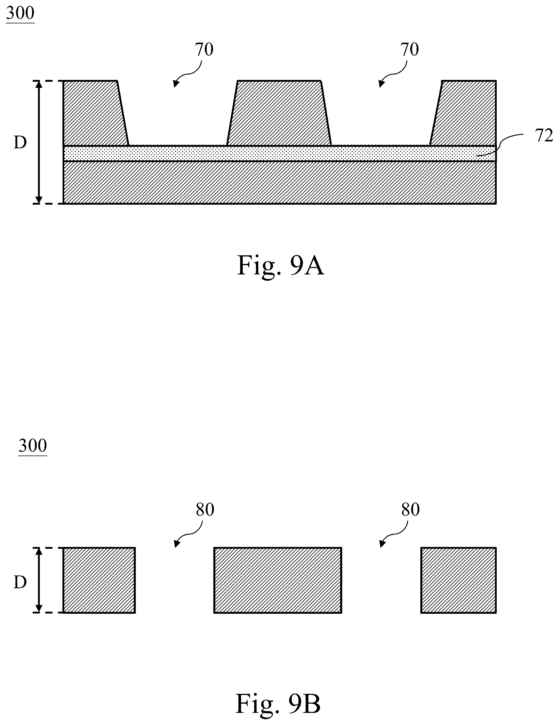
[0011] According to the other embodiment, the present invention provides a high-speed electroplating method, and the method includes the following steps: providing a component containing a gap between two adjacent metal parts; performing a pretreatment process to clean the component; disposing the component in an electroplating solution; and turning on an ultrasonic oscillation machine to vibrate the electroplating solution, and turning on a jet flow device to agitate the electroplating solution, and performing a pre-electroplating process with a plating current density of 0.5 A/dm.sup.2 to 5 A/dm.sup.2, and then performing a high-speed electroplating process to fill the gap with a plating current density of 6 A/dm.sup.2 to 100 A/dm.sup.2 to metallize the gap.
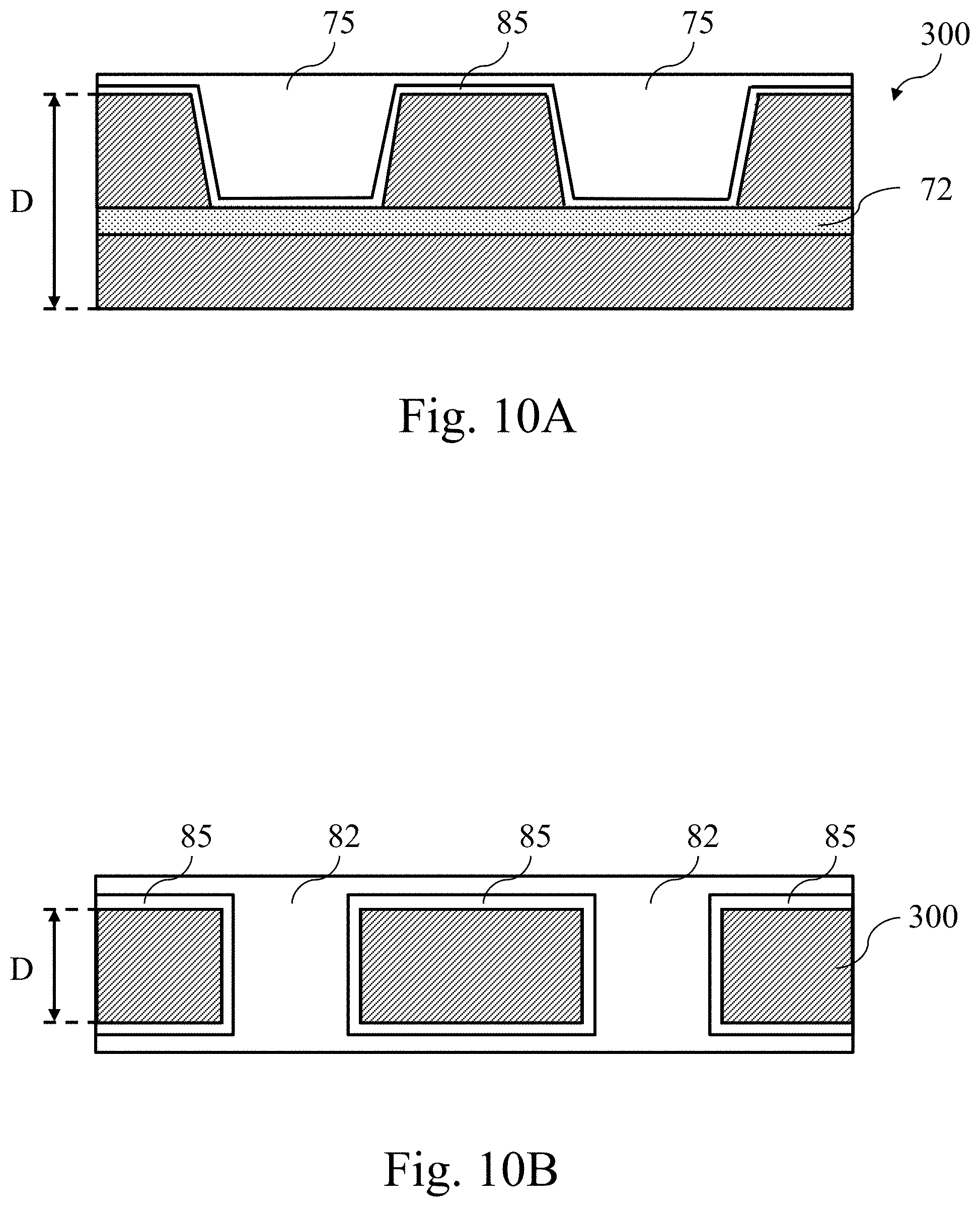
[0012] As described above, and the difference between the conventional technology and the present invention is that performing high plating current density electroplating by disposing a substrate or a component in an electroplating solution vibrated by ultrasonic waves and agitated by a jet flow.
[0013] By aforementioned technology means, the present invention may provide metal depositions with uniform microstructures.
BRIEF DESCRIPTION OF THE DRAWINGS
[0014] The invention will become more fully understood from the detailed description given herein below illustration only, and thus is not limitative of the present invention, and wherein:
[0015] FIG. 1 is a scanning electron microscopy image showing the cross-sectional view of a copper pillar deposited via high-speed electroplating;
[0016] FIG. 2 is a flowchart showing the steps for operating a high-speed electroplating method, according to the first embodiment of the present invention;
[0017] FIG. 3A is a schematic drawing of an embodiment of step 110 of FIG. 2;
[0018] FIG. 3B is a schematic drawing of an embodiment of step 120 of FIG. 2;
[0019] FIG. 3C is a schematic drawing of an embodiment of step 140 and step 150 of FIG. 2;
[0020] FIG. 3D is a schematic drawing of an embodiment of step 160 of FIG. 2;
[0021] FIG. 3E is a schematic drawing of an embodiment of step 170 of FIG. 2;
[0022] FIG. 4A is a top view schematic drawing of first embodiment of FIG. 3B;
[0023] FIG. 4B is a top view schematic drawing of second embodiment of FIG. 3B;
[0024] FIG. 5 is a flowchart showing steps for operating a high-speed electroplating method, according to the second embodiment of the present invention;
[0025] FIG. 6 is a schematic drawing of an embodiment of step 140 and step 350 of FIG. 5;
[0026] FIG. 7A is a scanning electron microscopy image showing the cross-sectional view of an embodiment of a copper pillar deposited via the high-speed electroplating method of FIG. 2;
[0027] FIG. 7B is a scanning electron microscopy image showing the cross-sectional view of an embodiment of a copper pillar deposited via the high-speed electroplating method of FIG. 5;
[0028] FIG. 8 is a flowchart showing steps for operating a high-speed electroplating method according to the third embodiment of the present invention;
[0029] FIG. 9A is a schematic drawing of an embodiment of a blind-hole structure of step 420 of FIG. 8;
[0030] FIG. 9B is a schematic drawing of an embodiment of a through-hole structure of step 420 of FIG. 8;
[0031] FIG. 10A is a schematic drawing of an embodiment of a blind-hole filling via the blind-hole structure of step 460 of FIG. 8;
[0032] FIG. 10B is a schematic drawing of an embodiment of a through-hole filling via the through-hole structure of step 460 of FIG. 8;
[0033] FIG. 11 is a flowchart showing steps for operating a high-speed electroplating method according to the fourth embodiment of the present invention;
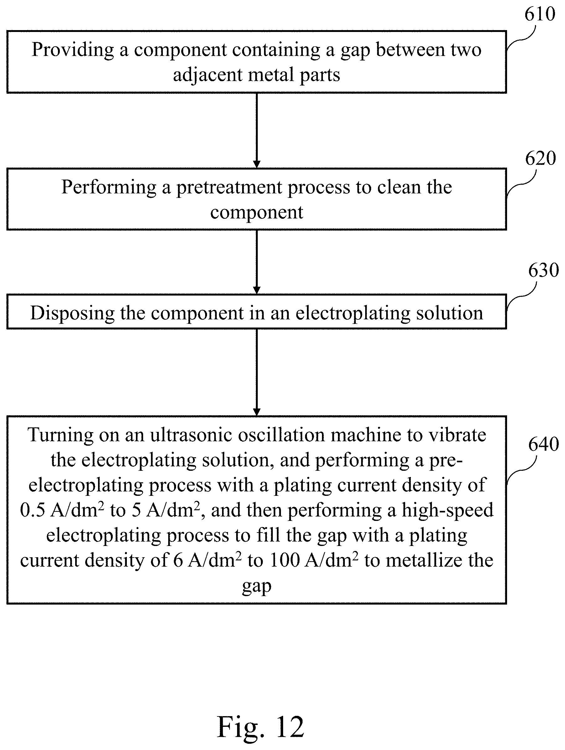
[0034] FIG. 12 is a flowchart showing steps for operating a high-speed electroplating method according to the fifth embodiment of the present invention;
[0035] FIG. 13A is a schematic drawing of an embodiment of a component containing a gap between two adjacent metal parts of step 610 of FIG. 12;
[0036] FIG. 13B is a schematic drawing of an embodiment of metallization of the gap of step 640 of FIG. 12; and
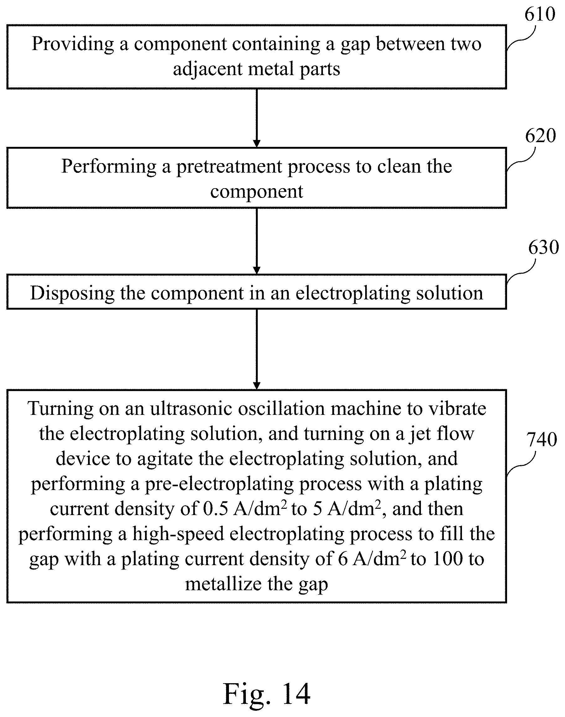
[0037] FIG. 14 is a flowchart showing steps for operating a high-speed electroplating method according to the sixth embodiment of the present invention.
DETAILED DESCRIPTION
[0038] The following embodiments of the present invention are herein described in detail with reference to the accompanying drawings. These drawings show specific examples of the embodiments of the present invention. It is to be understood that these embodiments are exemplary implementations and are not to be construed as limiting the scope of the present invention in any way. Further modifications to the disclosed embodiments, as well as other embodiments, are also included within the scope of the appended claims. These embodiments are provided so that this disclosure is thorough and complete, and fully conveys the inventive concept to those skilled in the art. Regarding the drawings, the relative proportions and ratios of elements in the drawings may be exaggerated or diminished in size for the sake of clarity and convenience. Such arbitrary proportions are only illustrative and not limiting in any way. The same reference numbers are used in the drawings and description to refer to the same or like parts.
[0039] As used herein, the term "or" includes any and all combinations of one or more of the associated listed items.
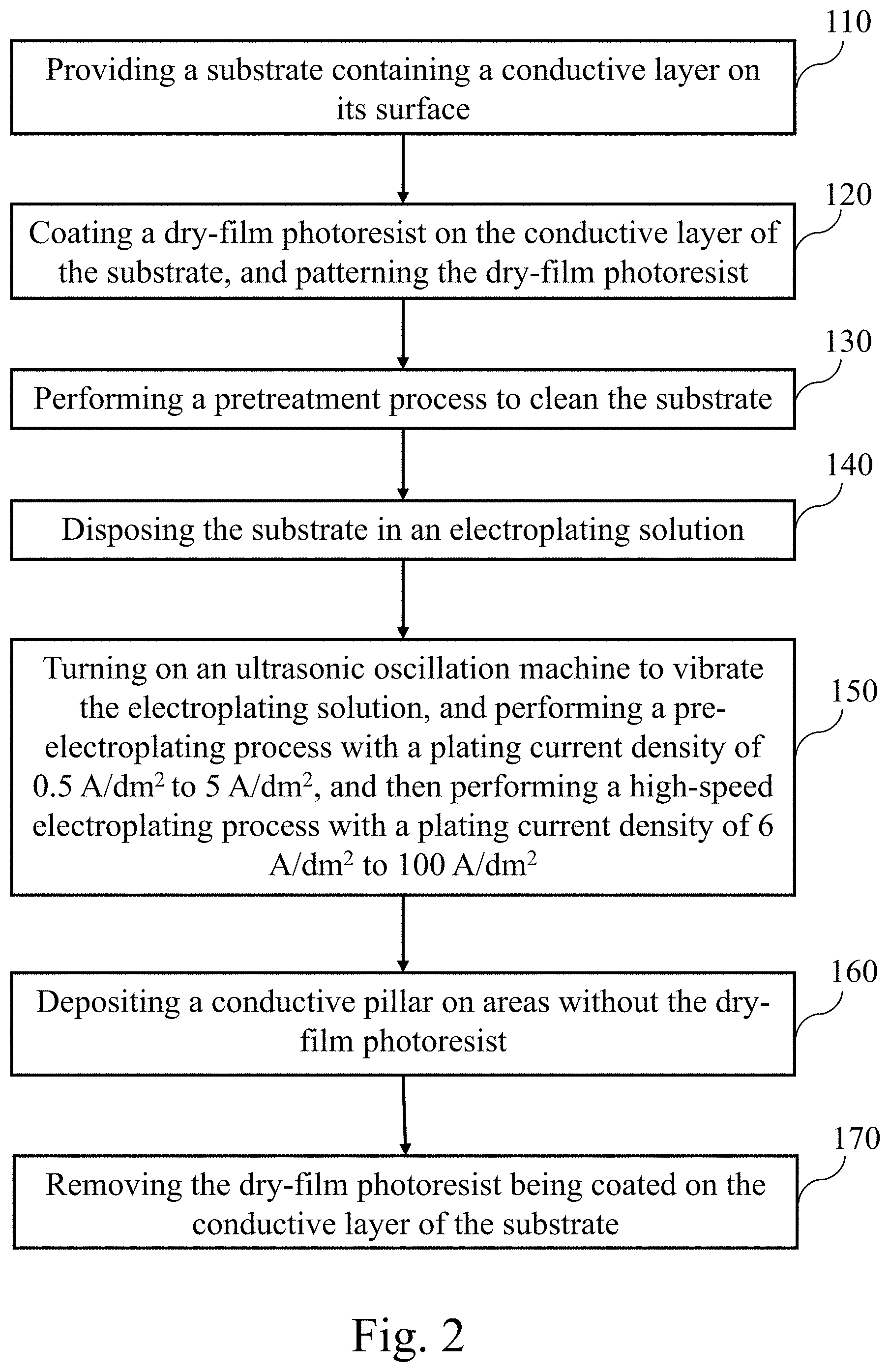
[0040] Please refer to FIG. 2 and FIGS. 3A to 3E, wherein FIG. 2 is a flowchart showing steps for operating a high-speed electroplating method according to the first embodiment of the present invention, and FIGS. 3A to 3E are schematic drawings of an embodiment of steps 110, 120, 140 and 150, 160, and 170 of the high-speed electroplating method of FIG. 2. In this embodiment, the high-speed electroplating method includes the following steps: providing a substrate containing a conductive layer on its surface (step 110); coating a dry-film photoresist on the conductive layer of the substrate, and patterning the dry-film photoresist (step 120); performing a pretreatment process to clean the substrate (step 130); disposing the substrate in an electroplating solution (step 140); turning on an ultrasonic oscillation machine to vibrate the electroplating solution, and performing a pre-electroplating process with a plating current density of 0.5 A/dm.sup.2 to 5 A/dm.sup.2, and then performing a high-speed electroplating process with a plating current density of 6 A/dm.sup.2 to 100 A/dm.sup.2 (step 150); depositing a conductive pillar on areas without the dry-film photoresist (step 160); and removing the dry-film photoresist being coated on the conductive layer of the substrate (step 170).
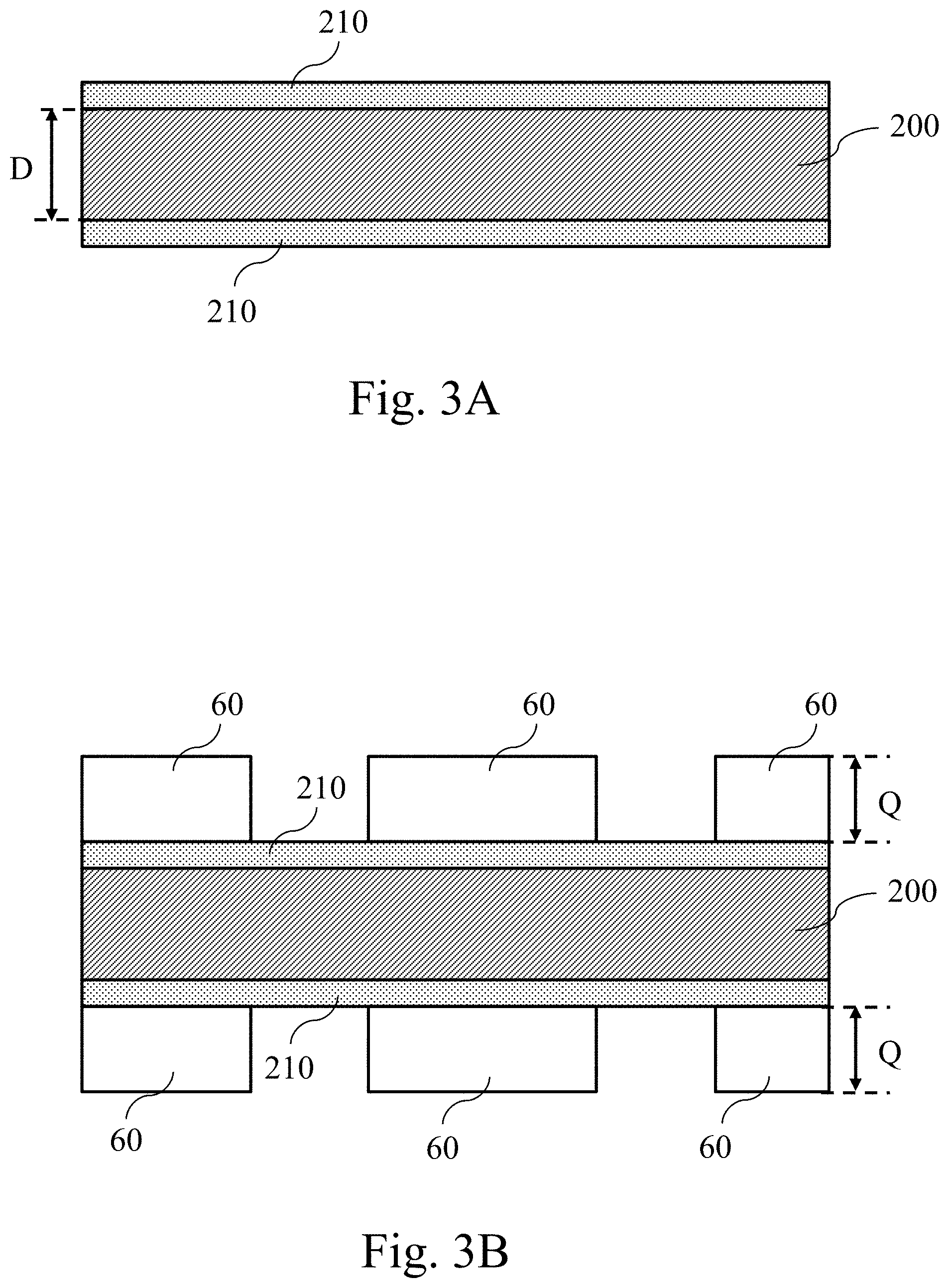
[0041] Please refer to FIG. 2 and FIG. 3A. In step 110, the thickness D of the substrate 200 may be, but not limited to, 0.2 to 1 millimeter (mm), and the substrate 200 may be the bismaleimide triazine (BT) substrate, the flame retardant 4 (FR4) substrate, the copper substrate or the ajinomoto build-up films (ABF) substrate, and the material of the substrate 200 may be, but not limited to, selected from the group consisting of glass fiber, epoxy resin, polyphenylene oxide (PPO), polyimide (PI), and polypropylene (PP). In this embodiment, the substrate 200 may be, but not limited to, a printed circuit board. There is a conductive layer 210 formed on the double-sided surfaces of the substrate 200 respectively. However, this embodiment is not intended to limit the present invention, and may be adjusted according to actual requirements. For example, there is a conductive layer 210 only formed on the single-sided surface of the substrate 200. Since the substrate 200 is a non-conductor, it is required to perform an electroless plating process, a physical vapor deposition (PVD) process or a chemical vapor deposition (CVD) process on the surface thereof, so that the surface of the substrate 200 has a conductive layer 210 to facilitate subsequent electroplating. Electroplating is performed on the conductive layer 210 to form a conductive pillar 50. The material of the conductive layer 210 may be selected from the group consisting of silver, gold, nickel, cobalt, palladium and copper, and may be adjusted according to actual requirements.
[0042] Please refer to FIG. 2 and FIG. 3B. Since the conductive pillars 50 are to be deposited on the conductive layer 210 of the substrate 200 instead of being electroplated with a metal film on the conductive layer 210, in step 120, the dry-film photoresist 60 may be uniformly attached to the conductive layer 210 through a laminator. In this embodiment, the dry-film photoresist 60 may be a negative dry-film photoresist, and then perform an exposure and development process on the dry-film photoresist 60 by using a correspondingly shaped mask (i.e., patterning the dry-film photoresist 60) according to the user's requirement for the appearance of the conductive pillars 50 (i.e., the shape of the bottom surface of each conductive pillar 50) to make the exposed dry-film photoresist 60 be polymerized and hardened, and make the unexposed dry-film photoresist 60 be the original monomers and be stripped by the developer, and then patterning the dry-film photoresist 60 according to the shape of the mask and creating the required appearance of the conductive pillar 50 (i.e., the shape of the bottom surface of the conductive pillar 50), but this embodiment is not intended to limit the invention. For example, the dry-film photoresist 60 may be a positive dry-film photoresist. When an exposure and development process is performed on the dry-film photoresist 60, the exposed dry-film photoresist 60 is decomposed and then may be stripped by the developer, and the dry-film photoresist 60 is patterned according to the shape of the mask and the required appearance of the conductive pillar 50 (i.e., the shape of the bottom surface of the conductive pillar 50) is created.
[0043] In addition, since the height of the conductive pillar 50 is less than or equal to the height Q of the dry-film photoresist 60 attached to the conductive layer 210, when the dry-film photoresist 60 is uniformly attached to the conductive layer 210 through the laminator, it should be noted that the height Q of the dry-film photoresist 60 uniformly attached to the conductive layer 210 conforms to the user's requirement of the conductive pillars 50 (that is, the height Q of the dry-film photoresist 60 uniformly attached to the conductive layer 210 needs to be greater than or equal to the height Q of the conductive pillar 50 on the conductive layer 210 the user expects).
[0044] In this embodiment, the expected conductive pillars 50 may be cylindrical pillars, so that the expected appearance of the conductive pillars 50 (i.e., the shape of the bottom surface of the conductive pillars 50) may be a circle (as shown in FIG. 4A, which is a top view schematic drawing of first embodiment of FIG. 3B). The diameter of the circle may be, but not limited to, 120 micrometers (.mu.m) to 10 millimeters (mm), but this embodiment is not intended to limit the invention, and may be adjusted according to actual requirements. For example, the expected conductive pillars 50 may be a square pillar, so that the expected appearance of the conductive pillars 50 (i.e., the shape of the bottom surface of the conductive pillars 50) may be a square (as shown in FIG. 4B, which is a top view schematic drawing of second embodiment of FIG. 3B), and the side length of the square may be, but not limited to, 120 .mu.m to 10 mm.
[0045] Please refer to FIG. 2, the pretreatment process described in step 130 may include: sequentially cleaning the conductive layer 210 of the substrate 200 with water, a detergent and pickle liquor. More specifically, the pretreatment process may clean the stains on the conductive layer 210 and remove the oxide layer on the surface thereof, and prevent bubbles from being left on the conductive layer 210. Water may be, but not limited to, deionized water. It should be noted that when the pickle liquor used for pickling and cleaning does not contain metallic ions of the electroplating solution, the conductive layer 210 of the substrate 200 may be washed again with water to avoid affecting the quality of the subsequent electroplating metal, and then the procedure of the subsequent steps 140 to 170 is performed.
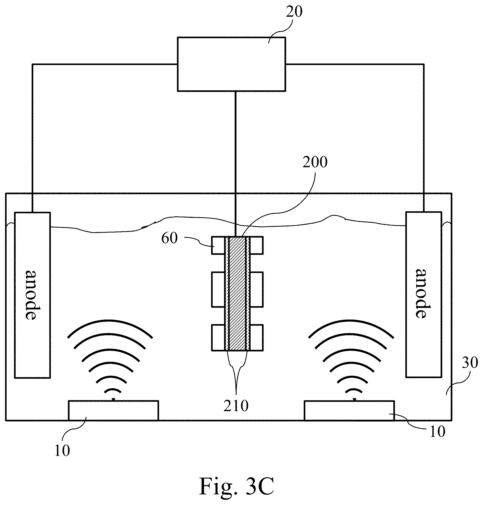
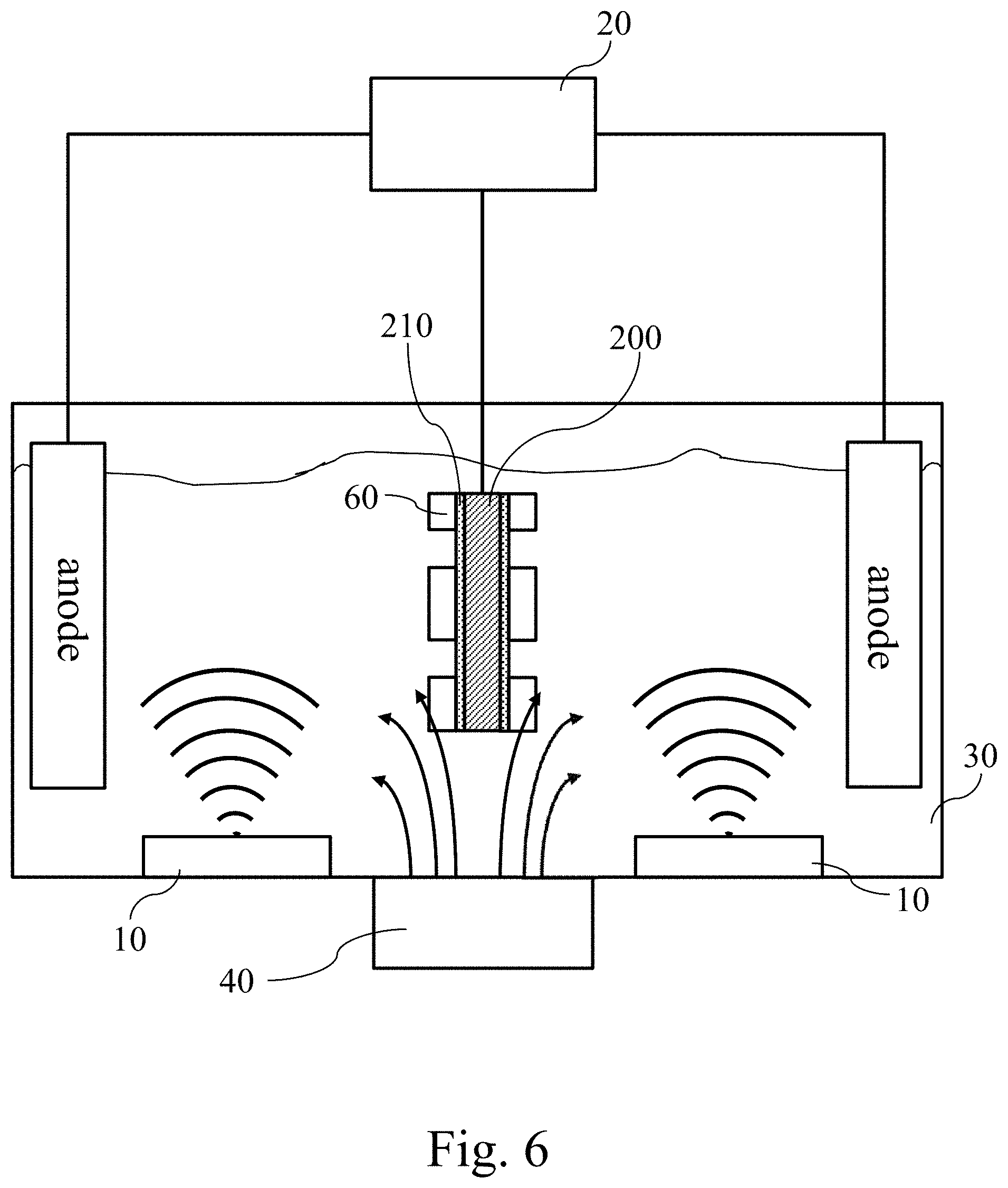
[0046] Next, please refer to FIG. 2, FIG. 3C and FIG. 3D. After performing the exposure development process (i.e., step 120) and the pretreatment process (i.e., step 130), the substrate 200 having the conductive layer 210 and the patterned dry-film photoresist 60 is disposed in the electroplating solution 30 (i.e., step 140), and the ultrasonic oscillating device 10 is turned on to vibrate the electroplating solution 30 and the power supply device 20 is used to perform the pre-electroplating process with the plating current density of 0.5 A/dm.sup.2 to 5 A/dm.sup.2, and then perform the high-speed electroplating process with the plating current density of 6 A/dm.sup.2 to 100 A/dm.sup.2 (i.e., step 150), that is, performing the high-speed electroplating with ultrasonic waves, thereby depositing the conductive pillars 50 on areas where the conductive layer 210 is not coated with the dry-film photoresist 60 (i.e., step 160). When step 140 is performed, the substrate 200 having the conductive layer 210 and the patterned dry-film photoresist 60 is disposed at the position of the cathode, and the position of the anode may be configured with a soluble anode, which is used to supplement the consumption of metallic ions of the electroplating solution, or an insoluble anode, such as a titanium net and an iridium/tantalum oxide composite anode. In the embodiment, the anode may be, but not limited to, an iridium/tantalum oxide composite insoluble anode. In addition, since double-sided electroplating is to be performed in the embodiment, the position of the substrate 200 containing the conductive layer 210 and the patterned dry-film photoresist 60 may be located at the center of the electroplating bath, and two anodes are disposed at the both sides of the electroplating bath. In the embodiment, the metallic ions in the electroplating solution 30 may be selected from the group consisting of silver ions, gold ions, nickel ions, cobalt ions, palladium ions and copper ions, and may be adjusted according to the material of the conductive pillars 50 that is expected to be deposited. During the high-speed electroplating process with ultrasonic waves (i.e., step 150), the power supply device 20 may be used to perform the pre-electroplating process with the plating current density of 0.5 A/dm.sup.2 to 5 A/dm.sup.2, and then increase the plating current density (i.e., the plating current density is 6 A/dm.sup.2 to 100 A/dm.sup.2) to perform the high-speed electroplating to reduce the required time for electroplating.
[0047] According to Faraday's law,
.delta. = M .times. .eta. z .times. F .times. .rho. .times. j .times. t , ##EQU00001##
wherein .delta. is the height of the conductive pillar 50 (unit: .mu.m), j is the plating current density (unit: A/dm.sup.2), t is the electroplating time (unit: minute), .eta. is the current efficiency, M is the molecular weight (unit: g/mol), z is the valence of the metal (i.e., the number of electrons transferred in each metallic ion), F is the Faraday constant (i.e., 96485 C/mol), and .rho. is the density of the electrolyte, it is known that the required time for electroplating may be derived from the plating current density and the height of the conductive pillar 50 that is expected to be deposited via electroplating. In the embodiment, it is expected that the height of the conductive pillars 50 deposited via electroplating may be 130 .mu.m to 500 .mu.m. For example, when it is expected that the conductive pillars 50 deposited via electroplating may be copper pillars, and the height of the conductive pillars 50 may be 168 .mu.m, Faraday's law shows that the corresponding formula is .delta.=0.22.times.j.times.t, so it may be pre-electroplated for approximately 15 minutes with the plating current density of 3 A/dm.sup.2 to deposit 10 .mu.m copper pillars, and then electroplated for approximately 9 minutes with the plating current density of 5 A/dm.sup.2 to deposit 10 .mu.m copper pillars (at this time, the height of each copper pillar is 20 .mu.m), and then electroplated for approximately 56 minutes with the plating current density of 12 A/dm.sup.2 to deposit 148 .mu.m copper pillars (at this time, the height of each copper pillar is 168 .mu.m).
[0048] In addition, in the embodiment, the ultrasonic oscillation of the electroplating solution is controlled to a frequency of 5 kilohertz (KHz) to 100 KHz, and the electroplating solution 30 may contain, in addition to copper ions, a solvent (e.g., water and sulfuric acid) and additives (e.g., brightener, carrier, leveler, wetting agent, and chloride ions).
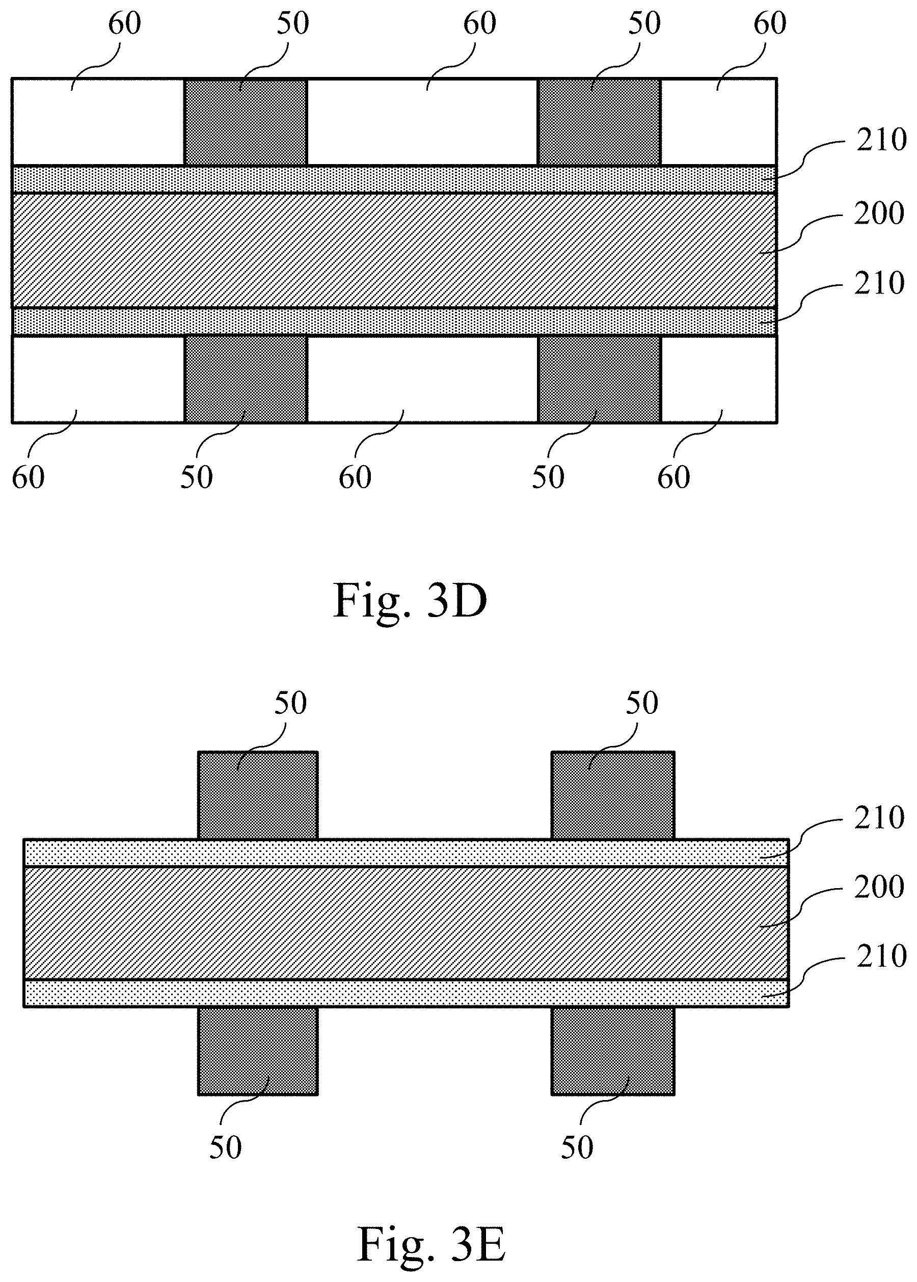
[0049] Next, please refer to FIG. 2 and FIG. 3E. After the conductive pillars 50 with the expected height is obtained according to the plating current density and the corresponding electroplating time, tetrahydrofuran (THF) or sodium hydroxide (NaOH) may be used to strip the patterned dry-film photoresist 60 be coating on the conductive layer 210 to reveal the conductive pillars 50 deposited via electroplating.
[0050] In addition, the electroplating layer would be deposited in a slower rate when the temperature of the electroplating solution 30 is lower than 25.degree. C., and the additive is unstable when the temperature of the electroplating solution 30 is higher than 30.degree. C. Thus, in this embodiment, the high-speed electroplating method may further include the step of controlling the temperature of the electroplating solution to be 25.degree. C. to 30.degree. C. through a temperature control device (not drawn).
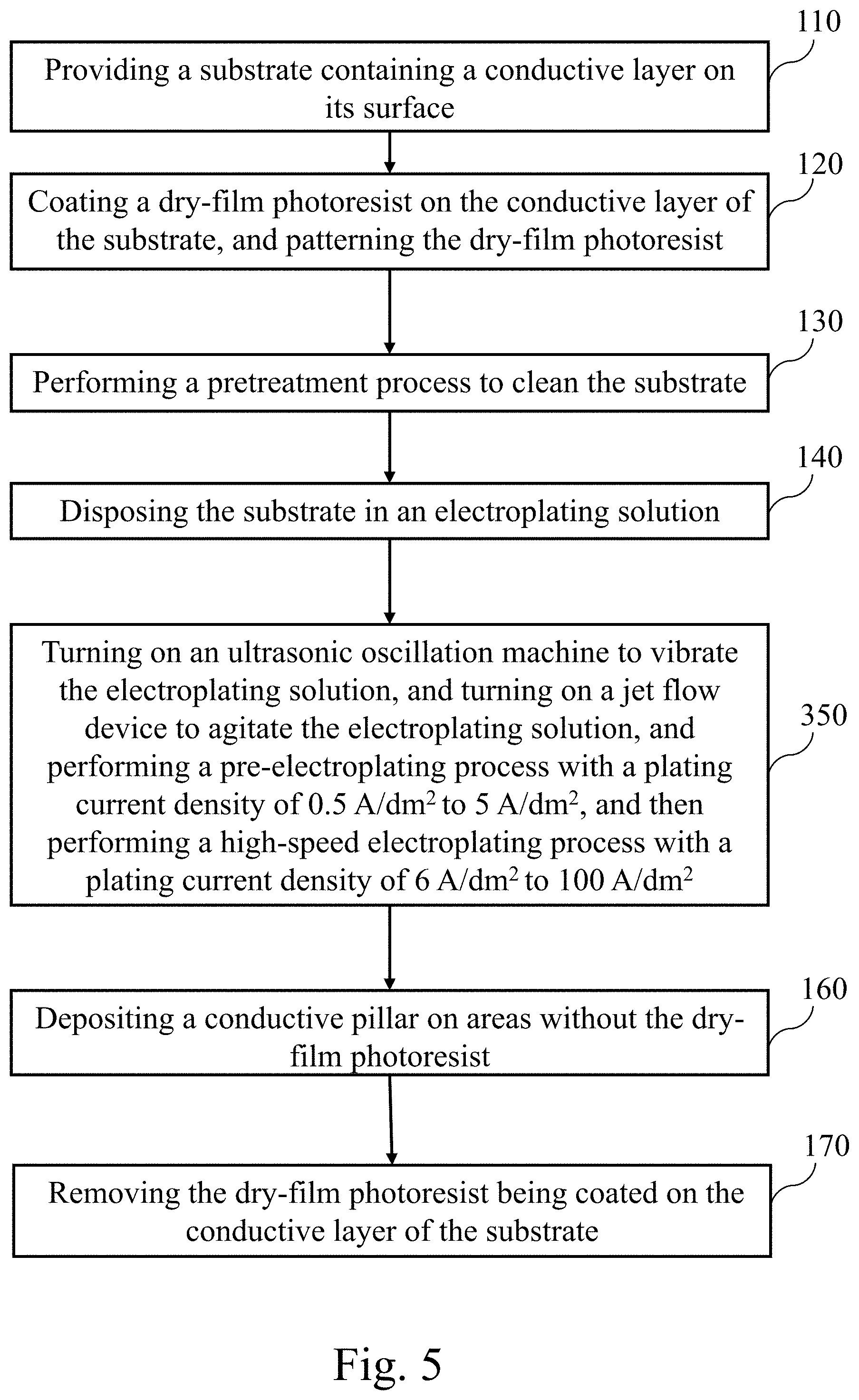
[0051] Please refer to FIG. 5, which is a flowchart showing steps for operating a high-speed electroplating method according to the second embodiment of the present invention, the high-speed electroplating method includes the following steps: providing a substrate containing a conductive layer on its surface (step 110); coating a dry-film photoresist on the conductive layer of the substrate, and patterning the dry-film photoresist (step 120); performing a pretreatment process to clean the substrate (step 130); disposing the substrate in an electroplating solution (step 140); turning on an ultrasonic oscillation machine to vibrate the electroplating solution, and turning on a jet flow device to agitate the electroplating solution, and performing a pre-electroplating process with a plating current density of 0.5 A/dm.sup.2 to 5 A/dm.sup.2, and then performing a high-speed electroplating process with a plating current density of 6 A/dm.sup.2 to 100 A/dm.sup.2 (step 350); depositing a conductive pillar on areas without the dry-film photoresist (step 160); and removing the dry-film photoresist being coated on the conductive layer of the substrate (step 170).
[0052] In other words, the difference between this embodiment and the first embodiment is that the high-speed electroplating method of this embodiment may further include the step of: turning on the jet flow device 40 to agitate the electroplating solution 30 (as shown in FIG. 6, which is a schematic drawing of an embodiment of step 140 and step 350 of FIG. 5) to improve the fluidity of the electroplating solution 30 and enhance mixing effect. The jet flow rate of the jet flow device 40 may be, but not limited to, less than or equal to 10 liters per minute.
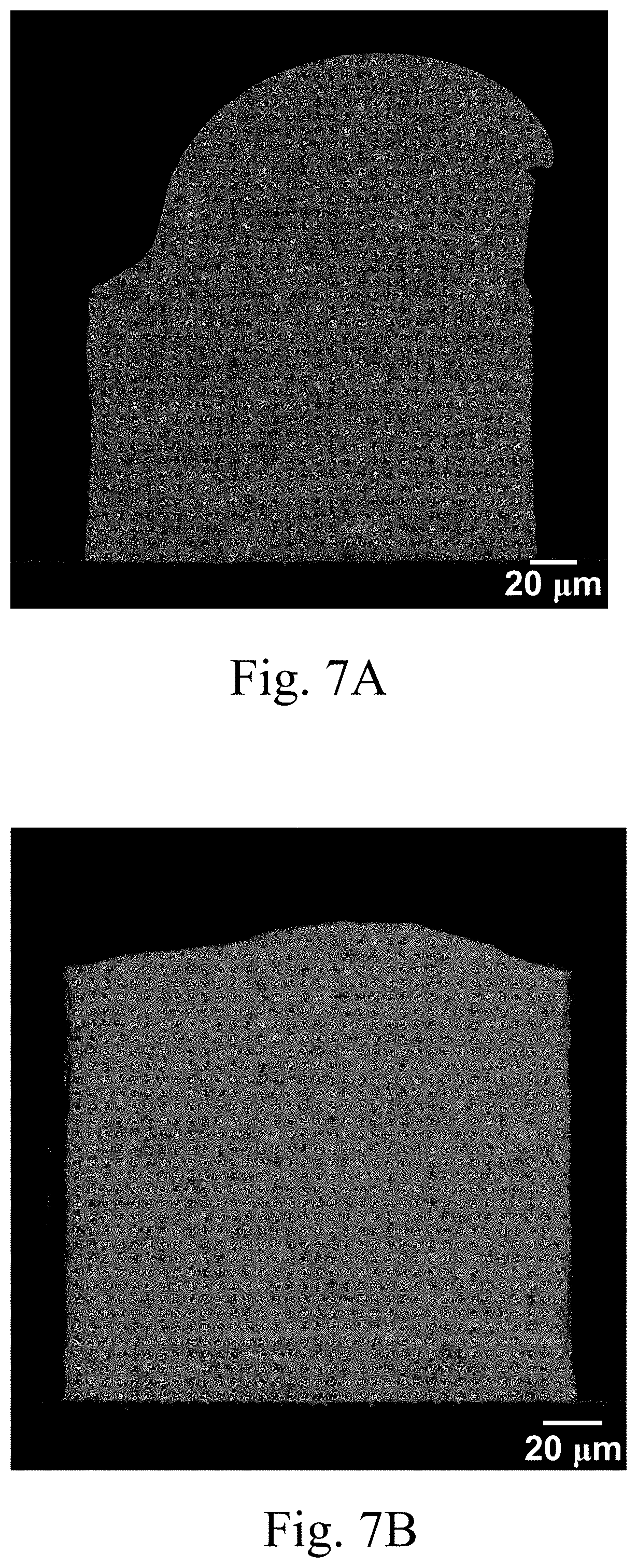
[0053] Please refer to FIG. 7A and FIG. 7B, wherein FIG. 7A is a scanning electron microscopy image showing the cross-sectional view of an embodiment of a copper pillar deposited via the high-speed electroplating method of FIG. 2, and FIG. 7B is a scanning electron microscopy image showing the cross-sectional view of an embodiment of a copper pillar deposited via the high-speed electroplating method of FIG. 5.
[0054] In FIG. 7A, it may be known that the copper pillar deposited via the high-speed electroplating method of FIG. 2 has relatively uniform grain sizes, which solves the problem that the copper pillar deposited via the conventional high-speed electroplating has non-uniform grain sizes and solves the problem of smaller grains in the upper region. Due to the cavitation of the ultrasonic waves, the electroplating solution may be more fully entered into the hole (that is, the groove formed by the conductive layer and the patterned dry-film photoresist), and the copper ions and additives may be immediately replenished to enhance the mass transfer in the hole. Thus, the copper pillar deposited via the high-speed electroplating method of FIG. 2 has relatively uniform grain sizes. In FIG. 7B, it may be known that the copper pillar deposited via the high-speed electroplating method of FIG. 5 not only has relatively uniform grain sizes but also has no necking which the copper pillar deposited via the high-speed electroplating method of FIG. 2 has, thereby improving the mechanical properties of the overall copper pillar.
[0055] In addition, a series of indentation tests is performed on the copper pillar deposited via the high-speed electroplating method of FIG. 5 (as shown in FIG. 7B) and the copper pillar of FIG. 1 deposited via the conventional high-speed electroplating by a nanoindenter. The hardness of the copper pillar deposited via the high-speed electroplating method of FIG. 5 may be approximately 2.0 GPa to 2.2 GPa, the Young's modulus of the copper pillar deposited via the high-speed electroplating method of FIG. 5 may be approximately 98.9 GPa to 105.6 GPa, and the stiffness of the copper pillar deposited via the high-speed electroplating method of FIG. 5 may be approximately 2.48.times.10.sup.5 N/m to 2.61.times.10.sup.5 N/m. However, the hardness of the copper pillar deposited via conventional high-speed electroplating may be approximately 1.6 GPa to 1.7 GPa, the Young's modulus of the copper pillar deposited via conventional high-speed electroplating may be approximately 91.8 GPa to 104.6 GPa, and the stiffness of the copper pillar deposited via conventional high-speed electroplating may be approximately 2.16.times.10.sup.5 N/m to 2.57.times.10.sup.5 N/m. Therefore, it is known that the mechanical properties of the copper pillar deposited via the high-speed plating method of FIG. 5 are higher than those of copper pillar deposited via conventional high-speed electroplating.
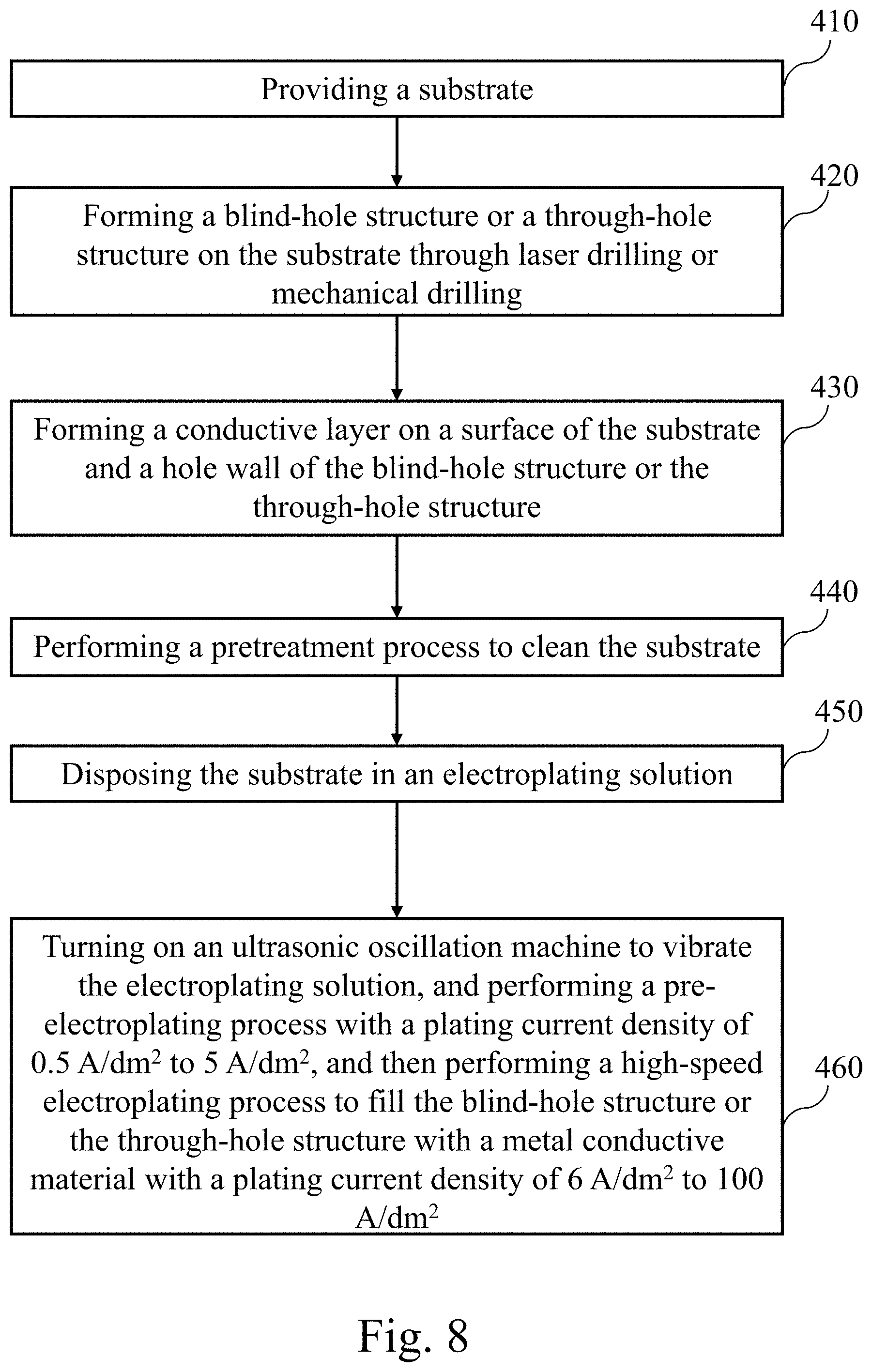
[0056] The high-speed electroplating method of the present invention may be used to form the above-mentioned conductive pillars, and further used to fill the blind-hole structure or the through-hole structure. For details, please refer to FIG. 8 to FIG. 10B, wherein FIG. 8 is a flowchart showing steps for operating a high-speed electroplating method according to the third embodiment of the present invention, FIG. 9A is a schematic drawing of an embodiment of a blind-hole structure of step 420 of FIG. 8, FIG. 9B is a schematic drawing of an embodiment of a through-hole structure of step 420 of FIG. 8, FIG. 10A is a schematic drawing of an embodiment of a blind-hole filling via the blind-hole structure of step 460 of FIG. 8, and FIG. 10B is a schematic drawing of an embodiment of a through-hole filling via the through-hole structure of step 460 of FIG. 8. In the embodiment, the high-speed electroplating method includes the following steps: providing a substrate (step 410); forming a blind-hole structure or a through-hole structure on the substrate through laser drilling or mechanical drilling (step 420); forming a conductive layer on a surface of the substrate and a hole wall of the blind-hole structure or the through-hole structure (step 430); performing a pretreatment process to clean the substrate (step 440); disposing the substrate in an electroplating solution (step 450); and turning on an ultrasonic oscillation machine to vibrate the electroplating solution, and performing a pre-electroplating process with a plating current density of 0.5 A/dm.sup.2 to 5 A/dm.sup.2, and then performing a high-speed electroplating process to fill the blind-hole structure or the through-hole structure with a metal conductive material with a plating current density of 6 A/dm.sup.2 to 100 A/dm.sup.2 (step 460).
[0057] In step 410, the thickness D of the substrate 300 may be, but not limited to, 0.2 mm to 3 mm, and the substrate 300 may be the BT substrate, the FR4 substrate, the copper substrate or the ABF substrate, and the material of the substrate 300 may be, but not limited to, selected from the group consisting of glass fiber, epoxy resin, PPO, PI, and PP. In this embodiment, the substrate 300 may be, but not limited to, a printed circuit board.
[0058] In step 420, the blind-hole structures 70 (as shown in FIG. 9A) or the through-hole structures 80 (such as FIG. 9B) are formed on the substrate 300 through a laser drilling process or a mechanical drilling process. The number and location of the blind-hole structures 70 or the through-hole structures 80 may be adjusted according to actual requirements. When the blind-hole structure 70 is a circular blind hole (that is, its top view is a circle), the diameter of the circle may be 50 .mu.m to 200 .mu.m, and the AR value (i.e., the aspect ratio, the ratio of the thickness of the substrate 300 to the diameter of the circle) may be 0.5 to 4.0. When the through-hole structure 80 is a circular through hole (that is, its top view is a circle), the diameter of the circle may be 50 .mu.m to 200 .mu.m, and the AR value may be 1.0 to 20. In addition, the substrate 300 may have a bottom copper layer 72 for conducting the blind-hole structures 70 respectively, and the bottom copper layer 72 may be formed by a lamination process or an electroless plating process.
[0059] In step 430, since the substrate 300 is a non-conductor, it is required to perform an electroless plating process, a physical vapor deposition (PVD) process or a chemical vapor deposition (CVD) process to make the surface of the substrate 300 and the hole wall of the blind-hole structures 70 or the through-hole structures 80 with the conductive layer 85 to facilitate subsequent electroplating for blind-hole/through-hole fillings. The material of the conductive layer 85 may be selected from the group consisting of silver, gold, nickel, cobalt, palladium and copper. The thickness of the conductive layer 85 may be, but not limited to, 1 .mu.m.
[0060] In step 440, the pretreatment process may include: sequentially cleaning the surface of the substrate 300 and the hole wall of the blind-hole structures 70 or the hole wall of the through-hole structures 80 with water, a detergent and pickle liquor. More specifically, the pretreatment process may clean the stains on the conductive layer 85 and remove the oxide layer on the surface thereof, and prevent bubbles from being left on the conductive layer 85. Water may be, but not limited to, deionized water. It should be noted that when the pickle liquor used for pickling and cleaning does not contain metallic ions of the electroplating solution, the conductive layer 85 of the substrate 300 may be washed again with water to avoid affecting the quality of the subsequent electroplating metal, and then the procedure of the subsequent steps 450 to 460 is performed.
[0061] After step 410 to step 440 are performed, the substrate 300 is disposed in the electroplating solution (i.e., step 450), and the ultrasonic oscillating device is turned on to vibrate the electroplating solution, and the power supply device is used to perform the pre-electroplating process with the plating current density of 0.5 A/dm.sup.2 to 5 A/dm.sup.2, and then perform the high-speed electroplating process to fill the blind-hole structures 70 or the through-hole structures 80 with a conductive material with the plating current density of 6 A/dm.sup.2 to 100 A/dm.sup.2 (i.e., step 460). When step 450 is performed, the substrate 300 is disposed at the position of the cathode, and the position of the anode may be configured with a soluble anode, which is used to supplement the consumption of metallic ions of the electroplating solution, or an insoluble anode, such as a titanium net and an iridium/tantalum oxide composite anode. In the embodiment, the anode may be, but not limited to, an iridium/tantalum oxide composite insoluble anode, the metallic ions in the electroplating solution 30 may be selected from the group consisting of silver ions, gold ions, nickel ions, cobalt ions, palladium ions and copper ions, and may be adjusted according to the material of the blind-holes/through-holes that are expected to be deposited. During the high-speed electroplating process with ultrasonic waves (i.e., step 460), the power supply device may be used to perform the pre-electroplating process with the plating current density of 0.5 A/dm.sup.2 to 5 A/dm.sup.2, and then increase the plating current density (i.e., the plating current density is 6 A/dm.sup.2 to 100 A/dm.sup.2) to perform the high-speed electroplating, wherein the times for the pre-electroplating process and perform the high-speed electroplating may be adjusted by actual requirements.
[0062] Due to the cavitation effect of the ultrasonic waves, the electroplating solution may be more fully entered into the blind-hole structure 70 or the through-hole structure 80, and the metallic ions and additives are immediately replenished, so that the blind-hole structure 70 or the through-hole structure 80 is filled with metal conductive material corresponding to the metallic ions, thereby depositing the blind-hole 75 (as shown in FIG. 10A) or the through-hole 82 (as shown in FIG. 10B), and avoiding appearance and structural defects (e.g., void formation and non-uniform grain distribution).
[0063] In addition, please refer to FIG. 11, which is a flowchart showing steps for operating a high-speed electroplating method according to the fourth embodiment of the present invention. The high-speed electroplating method may include the following steps: providing a substrate (step 410); forming a blind-hole structure or a through-hole structure on the substrate through laser drilling or mechanical drilling (step 420); forming a conductive layer on a surface of the substrate and a hole wall of the blind-hole structure or the through-hole structure (step 430); performing a pretreatment process to clean the substrate (step 440); disposing the substrate in an electroplating solution (step 450); and turning on an ultrasonic oscillation machine to vibrate the electroplating solution, and turning on a jet flow device to agitate the electroplating solution, and performing a pre-electroplating process with a plating current density of 0.5 A/dm.sup.2 to 5 A/dm.sup.2, and then performing a high-speed electroplating process to fill the blind-hole structure or the through-hole structure with a metal conductive material with a plating current density of 6 A/dm.sup.2 to 100 A/dm.sup.2 (step 560).
[0064] In other words, the difference between this embodiment and the third embodiment is that the high-speed electroplating method of this embodiment may further include the step of: turning on the jet flow device to agitate the electroplating solution to improve the fluidity of the electroplating solution and enhance mixing effect. The jet flow rate of the jet flow device may be, but not limited to, less than or equal to 10 liters per minute.
[0065] The high-speed electroplating method of the present invention may be used to deposit the above-mentioned conductive pillars and blind-holes/through-holes, and further used to metallize a gap (which may be applied to the three-dimensional (3D) integrated circuit (IC) packaging technology or the 3D electronic assembly). The technology of metallization of the gap may be used to directly remove the solder, and solve the damage problem caused by solder shrinkage or aging, and also avoid the formation of the brittle intermetallic compound joint (IMC joint) and the formation of microvoids in the micro joint. For details, please refer to FIGS. 12 to 13B, wherein FIG. 12 is a flowchart showing steps for operating a high-speed electroplating method according to the fifth embodiment of the present invention, FIG. 13A is a schematic drawing of an embodiment of a component containing a gap between two adjacent metal parts of step 610 of FIG. 12, and FIG. 13B is a schematic drawing of an embodiment of metallization of the gap of step 640 of FIG. 12. In this embodiment, the high speed electroplating method includes the following steps: providing a component containing a gap between two adjacent metal parts (step 610); performing a pretreatment process to clean the component (step 620); disposing the component in an electroplating solution (step 630); and turning on an ultrasonic oscillation machine to vibrate the electroplating solution, and performing a pre-electroplating process with a plating current density of 0.5 A/dm.sup.2 to 5 A/dm.sup.2, and then performing a high-speed electroplating process to fill the gap with a plating current density of 6 A/dm.sup.2 to 100 A/dm.sup.2 to metallize the gap (step 640).
[0066] In step 610, the component 400 has two or more metal parts 76, and the gap 90 is between two adjacent metal parts 76. The spacing of the gap 90 maybe, but not limited to, 10 .mu.m to 100 .mu.m. The material of the metal parts 76 may be selected from the group consisting of silver, gold, nickel, cobalt, palladium and copper, and the shape of the metal parts 76 may be circular or square. When the metal parts 76 are round metal parts (i.e., the top view is circular), the diameter may be 10 .mu.m to 200 .mu.m; when the metal parts 76 are square metal parts (that is, the top view thereof is square), the length and/or width may be 10 .mu.m to 200 .mu.m.
[0067] In step 620, the pretreatment process may include the step of: sequentially cleaning the component 400 with water, a detergent and pickle liquor. More specifically, the pretreatment process may clean the stains on the gap 90, remove the oxide layer on the surface thereof, and prevent bubbles from being left on the gap 90. Water may be, but not limited to, deionized water. It should be noted that, when the pickle liquor used for pickling and cleaning does not contain metallic ions of the electroplating solution, the gap 90 may be washed again with water to avoid affecting the quality of the subsequent electroplating metal, and then the procedure of the subsequent steps 630 to 640 is performed.
[0068] After step 610 to step 620 are performed, the component 400 is disposed in the electroplating solution (i.e., step 630), and the ultrasonic oscillating device is turned on to vibrate the electroplating solution, and the power supply device is used to perform the pre-electroplating process with the plating current density of 0.5 A/dm.sup.2 to 5 A/dm.sup.2, and then perform the high-speed electroplating process to fill the gap 90 with the plating current density of 6 A/dm.sup.2 to 100 A/dm.sup.2 to metallize the gap 90 (i.e., step 640). When step 630 is performed, the component 400 is disposed at the position of the cathode, and the position of the anode may be configured with a soluble anode, which is used to supplement the consumption of metallic ions of the electroplating solution, or an insoluble anode, such as a titanium net and an iridium/tantalum oxide composite anode. In the embodiment, the anode may be, but not limited to, an iridium/tantalum oxide composite insoluble anode, the metallic ions in the electroplating solution 30 may be selected from the group consisting of silver ions, gold ions, nickel ions, cobalt ions, palladium ions and copper ions, and may be adjusted according to actual requirements. During the high-speed electroplating process with ultrasonic waves (i.e., step 640), the power supply device may be used to perform the pre-electroplating process with the plating current density of 0.5 A/dm.sup.2 to 5 A/dm.sup.2, and then increase the plating current density (i.e., the plating current density is 6 A/dm.sup.2 to 100 A/dm.sup.2) to perform the high-speed electroplating, wherein the times for the pre-electroplating process and perform the high-speed electroplating may be adjusted by actual requirements.
[0069] Due to the cavitation effect of the ultrasonic waves, the electroplating solution may be more fully entered into the gap 90, and the metallic ions and additives are instantly replenished, so that the gap 90 is filled with metal conductive material corresponding to the metallic ions, thereby metallizing the gap 90 (as shown in FIG. 13B), and avoiding appearance and structural defects (e.g., void formation and non-uniform grain distribution).
[0070] In addition, please refer to FIG. 14, which is a flowchart showing steps for operating a high-speed electroplating method according to the sixth embodiment of the present invention. The high-speed electroplating method may include the following steps: providing a component containing a gap between two adjacent metal parts (step 610); performing a pretreatment process to clean the component (step 620); disposing the component in an electroplating solution (step 630); and turning on an ultrasonic oscillating device to vibrate the electroplating solution, and turning on a jet flow device to agitate the electroplating solution, and performing a pre-electroplating process with a plating current density of 0.5 A/dm.sup.2 to 5 A/dm.sup.2, and then performing a high-speed electroplating process to fill the gap with a plating current density of 6 A/dm.sup.2 to 100 A/dm.sup.2 to metallize the gap (step 740).
[0071] In other words, the difference between this embodiment and the fifth embodiment is that the high-speed electroplating method of this embodiment may further include the step of: turning on the jet flow device to agitate the electroplating solution to improve the fluidity of the electroplating solution and enhance mixing effect. The jet flow rate of the jet flow device may be, but not limited to, less than or equal to 10 liters per minute.
[0072] As described above, and the difference between the conventional technology and the present invention is that performing high plating current density electroplating by disposing a substrate or a component in an electroplating solution vibrated by ultrasonic waves, thereby solving the problem of microstructure inhomogeneity deposited via conventional high-speed electroplating, and providing metal depositions with uniform microstructures.
[0073] Although the invention has been described with reference to specific embodiments, this description is not meant to be construed in a limiting sense. Various modifications of the disclosed embodiments, as well as alternative embodiments, will be apparent to persons skilled in the art. It is, therefore, contemplated that the appended claims will cover all modifications that fall within the true scope of the invention.
* * * * *
D00000
D00001
D00002
D00003
D00004
D00005
D00006
D00007
D00008
D00009
D00010
D00011
D00012
D00013

D00014
D00015

D00016

XML
uspto.report is an independent third-party trademark research tool that is not affiliated, endorsed, or sponsored by the United States Patent and Trademark Office (USPTO) or any other governmental organization. The information provided by uspto.report is based on publicly available data at the time of writing and is intended for informational purposes only.
While we strive to provide accurate and up-to-date information, we do not guarantee the accuracy, completeness, reliability, or suitability of the information displayed on this site. The use of this site is at your own risk. Any reliance you place on such information is therefore strictly at your own risk.
All official trademark data, including owner information, should be verified by visiting the official USPTO website at www.uspto.gov. This site is not intended to replace professional legal advice and should not be used as a substitute for consulting with a legal professional who is knowledgeable about trademark law.