Memory Circuit And Formation Method Thereof
Tsai; Chun-Yang ; et al.
U.S. patent application number 16/583097 was filed with the patent office on 2020-01-23 for memory circuit and formation method thereof. The applicant listed for this patent is Taiwan Semiconductor Manufacturing Co., Ltd.. Invention is credited to Kuo-Ching Huang, Tong-Chern Ong, Chun-Yang Tsai.
| Application Number | 20200027922 16/583097 |
| Document ID | / |
| Family ID | 65234823 |
| Filed Date | 2020-01-23 |


View All Diagrams
| United States Patent Application | 20200027922 |
| Kind Code | A1 |
| Tsai; Chun-Yang ; et al. | January 23, 2020 |
MEMORY CIRCUIT AND FORMATION METHOD THEREOF
Abstract
The present disclosure, in some embodiments, relates to an integrated chip. The integrated chip includes a control device arranged within a substrate and having a terminal. A first memory device is coupled between the terminal of the control device and a first bit-line. A second memory device is coupled between the terminal of the control device and a second bit-line.
| Inventors: | Tsai; Chun-Yang; (Hsinchu City, TW) ; Huang; Kuo-Ching; (Hsinchu City, TW) ; Ong; Tong-Chern; (Taipei, TW) | ||||||||||
| Applicant: |
|
||||||||||
|---|---|---|---|---|---|---|---|---|---|---|---|
| Family ID: | 65234823 | ||||||||||
| Appl. No.: | 16/583097 | ||||||||||
| Filed: | September 25, 2019 |
Related U.S. Patent Documents
| Application Number | Filing Date | Patent Number | ||
|---|---|---|---|---|
| 15678557 | Aug 16, 2017 | 10461126 | ||
| 16583097 | ||||
| Current U.S. Class: | 1/1 |
| Current CPC Class: | G11C 11/1659 20130101; G11C 2013/0073 20130101; G11C 2013/0088 20130101; H01L 27/228 20130101; G11C 13/0069 20130101; G11C 2013/0071 20130101; G11C 2013/0042 20130101; G11C 2213/82 20130101; G11C 2213/78 20130101; H01L 45/1253 20130101; G11C 11/1673 20130101; G11C 11/1675 20130101; G11C 13/004 20130101; G11C 2213/71 20130101; G11C 2213/79 20130101; H01L 27/2436 20130101; G11C 13/003 20130101 |
| International Class: | H01L 27/24 20060101 H01L027/24; G11C 11/16 20060101 G11C011/16; G11C 13/00 20060101 G11C013/00; H01L 45/00 20060101 H01L045/00 |
Claims
1. An integrated chip, comprising: a control device arranged within a substrate and having a terminal; a first memory device coupled between the terminal of the control device and a first bit-line; and a second memory device coupled between the terminal of the control device and a second bit-line.
2. The integrated chip of claim 1, wherein the control device is a transistor having a gate structure laterally disposed between a source region and a drain region; and wherein the first memory device and the second memory device are coupled to the drain region.
3. The integrated chip of claim 1, wherein the first memory device comprises a first data storage layer over a first lower electrode and a first upper electrode over the first data storage layer, the first upper electrode coupled between the first data storage layer and the terminal; and wherein the second memory device comprises a second data storage layer over a second lower electrode and a second upper electrode over the second data storage layer, the second lower electrode coupled between the second data storage layer and the terminal.
4. The integrated chip of claim 1, further comprising: a plurality of interconnect layers disposed within a dielectric structure over the substrate and electrically coupling the terminal to the first memory device and the second memory device, wherein one of the plurality of interconnect layers is disposed directly between the first memory device and the second memory device.
5. The integrated chip of claim 1, further comprising: an interconnect wire disposed within a dielectric structure over the substrate and coupled between the terminal and the first memory device and between the terminal and the second memory device.
6. The integrated chip of claim 1, wherein the first memory device and the second memory device are configured to store complementary data states upon application of a same bias voltage at the terminal.
7. The integrated chip of claim 1, wherein the terminal is coupled to an upper surface of the first memory device and a lower surface of the second memory device.
8. The integrated chip of claim 7, further comprising: a sense amplifier having a first input selectively coupled to a lower surface of the first memory device and a second input selectively coupled to an upper surface of the second memory device.
9. The integrated chip of claim 1, further comprising: one or more isolation structures disposed within the substrate and laterally surrounding the control device, wherein the first memory device and the second memory device are laterally between opposing outermost sidewalls of the one or more isolation structures.
10. A memory circuit, comprising: a first memory device operably coupled between a source-line and a first bit-line; a second memory device operably coupled between the source-line and a second bit-line; and a sense amplifier operably coupled to the first bit-line and to the second bit-line.
11. The memory circuit of claim 10, wherein the sense amplifier has a first input operably coupled to the first bit-line and a second input operably coupled to the second bit-line.
12. The memory circuit of claim 10, wherein the first memory device comprises a first upper electrode disposed over a first lower electrode, the first lower electrode between the first bit-line and the first upper electrode; and wherein the second memory device comprises a second upper electrode disposed over a second lower electrode, the second upper electrode between the second bit-line and the second lower electrode.
13. The memory circuit of claim 10, further comprising: an access device coupled between the source-line and an interconnect structure coupled to both the first memory device and the second memory device.
14. The memory circuit of claim 10, further comprising: an access device having a first terminal coupled to the source-line and a second terminal between the first terminal and both the first memory device and the second memory device.
15. The memory circuit of claim 10, wherein the first memory device comprises a first capping layer coupled between the source-line and a first high k-dielectric data storage layer; and wherein the second memory device comprises a second high k-dielectric data storage layer coupled between the source-line and a second capping layer.
16. A memory circuit, comprising: a first memory device having a first terminal and a second terminal, the first terminal operably coupled to a source-line; a second memory device having a third terminal and a fourth terminal, the third terminal operably coupled to the source-line; and a sense amplifier having a first input coupled to the second terminal and a second input coupled to the fourth terminal.
17. The memory circuit of claim 16, further comprising: an access device having an input terminal coupled to the source-line and an output terminal coupled to both the first terminal and the second terminal.
18. The memory circuit of claim 16, further comprising: a dielectric structure disposed over a substrate and surrounding the first memory device and the second memory device, wherein a line that is perpendicular to an upper surface of the substrate vertically extends through the first memory device and the second memory device.
19. The memory circuit of claim 16, further comprising: a dielectric structure disposed over a substrate and surrounding the first memory device and the second memory device, wherein a line that is parallel to an upper surface of the substrate laterally extends through the first memory device and the second memory device.
20. The memory circuit of claim 16, wherein the first memory device and the second memory device respectively comprise a resistive random access memory device, a phase change memory device, a magneto-resistive memory device, or a ferroelectric random access memory device.
Description
REFERENCE TO RELATED APPLICATION
[0001] This application is a Continuation of U.S. application Ser. No. 15/678,557, filed on Aug. 16, 2017, the contents of which are hereby incorporated by reference in their entirety.
BACKGROUND
[0002] Many modern day electronic devices contain electronic memory configured to store data. Electronic memory may be volatile memory or non-volatile memory. Volatile memory stores data when it is powered, while non-volatile memory (NVM) is able to store data when power is removed. Unlike conventional NVM devices (e.g., flash, EEPROM, etc.), many promising candidates for a next generation NVM technology use memory cells that are located within a back-end-of-the-line (BEOL) of an integrated chip (e.g., located between metal interconnect layers overlying a semiconductor substrate).
BRIEF DESCRIPTION OF THE DRAWINGS
[0003] Aspects of the present disclosure are best understood from the following detailed description when read with the accompanying figures. It is noted that, in accordance with the standard practice in the industry, various features are not drawn to scale. In fact, the dimensions of the various features may be arbitrarily increased or reduced for clarity of discussion.
[0004] FIG. 1 illustrates a schematic diagram of some embodiments of a memory circuit having a shared control device configured to provide access to target and complementary memory devices.
[0005] FIG. 2 illustrates a cross-sectional view of some embodiments of a memory circuit having a shared control device configured to provide access to target and complementary memory devices.
[0006] FIGS. 3A-3D illustrate some embodiments of schematic diagrams showing operation of a disclosed memory circuit.
[0007] FIG. 4 illustrates a schematic diagram of some embodiments of a memory array having shared transistors for access to target and complementary memory devices.
[0008] FIG. 5 illustrates a cross-sectional view of some embodiments of an integrated chip having a shared transistor for access to target and complementary RRAM devices.
[0009] FIG. 6 illustrates a cross-sectional view of some alternative embodiments of an integrated chip having a shared transistor for access to target and complementary RRAM devices.
[0010] FIG. 7 illustrates a table showing some embodiments of operating conditions of a RRAM circuit having a shared transistor for access to target and complementary RRAM devices.
[0011] FIGS. 8A-8C illustrate flow diagrams of some embodiments of methods of operating a RRAM circuit having a shared transistor for access to target and complementary RRAM devices.
[0012] FIGS. 9-13 illustrate cross-sectional views of some embodiments of a method of forming an integrated chip comprising a memory circuit having a shared control device configured to provide access to target and complementary memory devices.
[0013] FIGS. 14-17 illustrate cross-sectional views of some alternative embodiments of a method of forming an integrated chip comprising a memory circuit having a shared control device configured to provide access to target and complementary memory devices.
[0014] FIG. 18 illustrates a flow diagram of some embodiments of a method of forming an integrated chip comprising a memory circuit having a shared control device configured to provide access to target and complementary memory devices.
DETAILED DESCRIPTION
[0015] The following disclosure provides many different embodiments, or examples, for implementing different features of the provided subject matter. Specific examples of components and arrangements are described below to simplify the present disclosure. These are, of course, merely examples and are not intended to be limiting. For example, the formation of a first feature over or on a second feature in the description that follows may include embodiments in which the first and second features are formed in direct contact, and may also include embodiments in which additional features may be formed between the first and second features, such that the first and second features may not be in direct contact. In addition, the present disclosure may repeat reference numerals and/or letters in the various examples. This repetition is for the purpose of simplicity and clarity and does not in itself dictate a relationship between the various embodiments and/or configurations discussed.
[0016] Further, spatially relative terms, such as "beneath," "below," "lower," "above," "upper" and the like, may be used herein for ease of description to describe one element or feature's relationship to another element(s) or feature(s) as illustrated in the figures. The spatially relative terms are intended to encompass different orientations of the device in use or operation in addition to the orientation depicted in the figures. The apparatus may be otherwise oriented (rotated 90 degrees or at other orientations) and the spatially relative descriptors used herein may likewise be interpreted accordingly.
[0017] In many modern day memory circuits, differential sensing is used to read data from a memory circuit. Differential sensing allows for a small signal to generate a strong output state. Differential sensing uses two data lines for each bit read from a memory cell. The first data line transits a first signal (e.g., a low signal) and the second data line transits a complementary second signal (e.g., a high signal). A difference between the first and second signals is determined by a sensing amplifier and a data state of "1" or "0" is determined from the difference. Differential sensing offers a number of advantages over single line sensing (e.g., sensing against a reference voltage), such as more accurate reading due to a greater tolerance to noise.
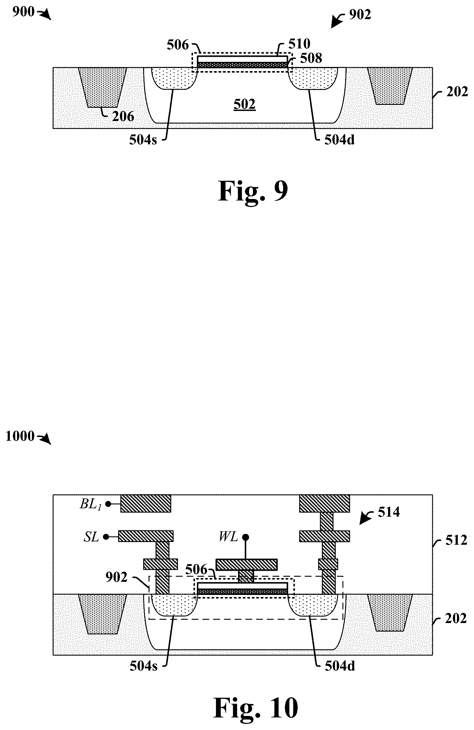
[0018] However, memory cells that use differential sensing generally have a larger cell size since the memory cells use both a target device and a complementary device to store a data state. The larger cell size causes memory arrays to consume a larger silicon area, thereby increasing an overall cost of an integrated chip. Furthermore, during operation of a memory array that uses differential sensing, data has to be written to both a target device and a complementary device to store a data bit, thereby driving a larger write time than single ended sensing schemes.
[0019] The present disclosure relates to a memory circuit having a shared control device for access to both target and complementary memory devices of a memory array configured to operate using differential sensing, and an associated method of formation. In some embodiments, the memory circuit has a control device arranged within a substrate. The control device has a first terminal coupled to a source-line, a second terminal coupled to a word-line, and a third terminal. A first memory device is arranged over the substrate and has a first lower electrode separated from a first upper electrode by a first data storage layer. The first upper electrode is coupled to the third terminal and the first lower electrode is coupled to a first bit-line. A second memory device is arranged over the substrate and has a second lower electrode separated from a second upper electrode by a second data storage layer. The second upper electrode is coupled to the second bit-line and the second lower electrode is coupled to the third terminal. By connecting the upper electrode of the first memory device and the lower electrode of the second memory device to a same control device, data can be concurrently written to both the first (e.g., target) and second (e.g., complementary) memory devices using a memory cell with a relatively small footprint.
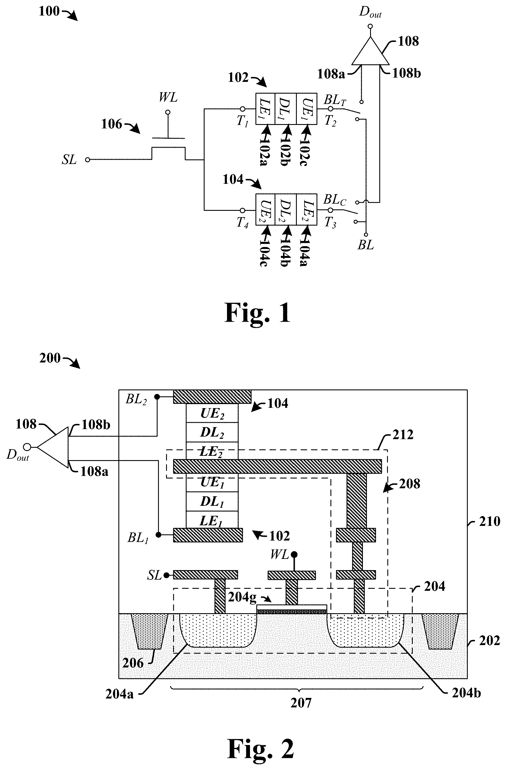
[0020] FIG. 1 illustrates a schematic diagram of some embodiments of a memory circuit 100 having a shared control device configured to provide access to both target and complementary memory devices.
[0021] The memory circuit 100 comprises a target memory device 102 and a complementary memory device 104 coupled between a shared source-line SL and parallel bit-lines, BL.sub.T and BL.sub.C. The target memory device 102 has a first lower electrode 102a coupled to a first terminal T.sub.1 and a first upper electrode 102c coupled to a second terminal T.sub.2. The first lower electrode 102a is separated from the first upper electrode 102c by way of a first data storage layer 102b. The complementary memory device 104 has a second lower electrode 104a coupled to a third terminal T.sub.3 and a second upper electrode 104c coupled to a fourth terminal T.sub.4. The second lower electrode 104a is separated from the second upper electrode 104c by way of a second data storage layer 104b.
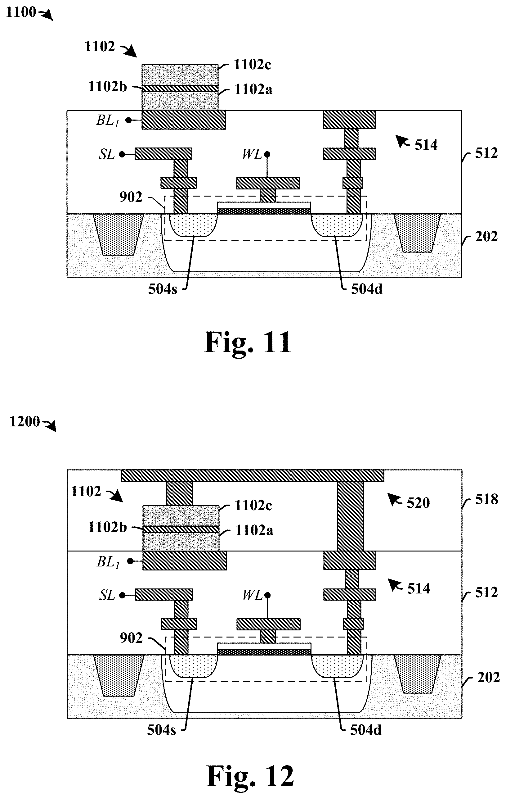
[0022] The target memory device 102 and the complementary memory device 104 are coupled to the shared source-line SL and to the bit-lines, BL.sub.T and BL.sub.C, in configurations that are inverted with respect to one another. For example, the first terminal T.sub.1 and the fourth terminal T.sub.4 are coupled to the shared source-line SL by way of a shared control device 106, so that the first lower electrode 102a and the second upper electrode 104c are coupled to the shared source-line SL. The second terminal T.sub.2 and the third terminal T.sub.3 are respectively coupled to the bit-lines, BL.sub.T and BL.sub.C, so that the first upper electrode 102c and the second lower electrode 104a may be selectively coupled to a first input 108a and a second input 108b of a sense amplifier 108 concurrently.
[0023] Coupling the target memory device 102 and the complementary memory device 104 to the shared source-line SL and the bit-lines, BL.sub.T and BL.sub.C, in inverted configurations will result in bias voltages of opposite polarities across the target memory device 102 and the complementary memory device 104. For example, during a write operation, the inverted configuration allows for a first potential difference to be applied between the first lower electrode 102a and the first upper electrode 102c of the target memory device 102 and a second potential difference having an opposite sign as the first potential difference to be applied between the second lower electrode 104a and the second upper electrode 104c of the complementary memory device 104. The opposite potential differences allow for different data states to be concurrently written in parallel to the target memory device 102 and the complementary memory device 104 using the shared control device 106, thereby providing the memory circuit 100 with a small size and fast write time.
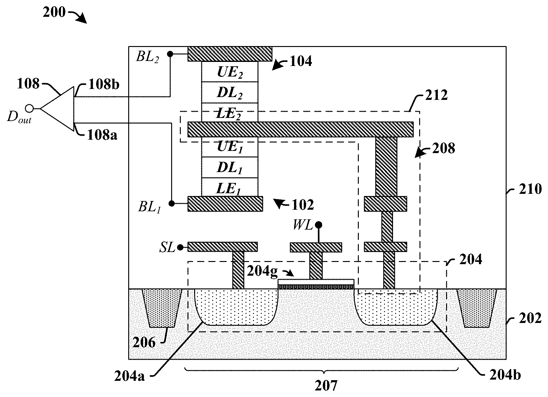
[0024] FIG. 2 illustrates a cross-sectional view of some embodiments of a memory circuit 200 having a shared control device configured to provide access to both target and complementary memory devices.
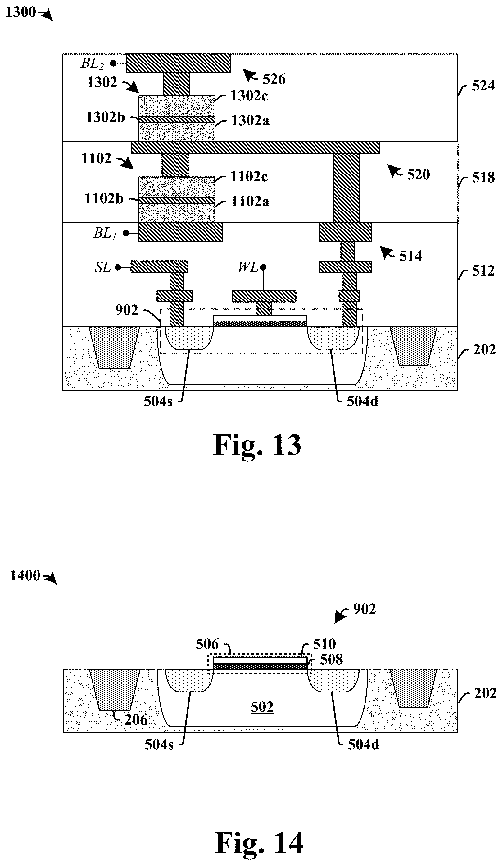
[0025] The memory circuit 200 comprises a shared control device 204 arranged within a substrate 202. In various embodiments, the shared control device 204 may comprise a MOSFET, a bi-polar junction transistor (BJT), a high electron mobility transistor (HEMT), or a similar device. The shared control device 204 has a first terminal coupled to a source-line SL, a second terminal coupled to a word-line WL, and a third terminal. In some embodiments, wherein the shared control device 204 comprises a MOSFET, the first terminal may comprise a first source/drain region 204a, the second terminal may comprise a gate structure 204g, and the third terminal may comprise a second source/drain region 204b. In some embodiments, the shared control device 204 may be arranged within a memory cell region 207 disposed between isolation regions 206 (e.g., shallow trench isolation regions) within the substrate 202.
[0026] A dielectric structure 210 is arranged over the substrate 202. A plurality of conductive interconnect layers 208 are surrounded by the dielectric structure 210. The plurality of conductive interconnect layers 208 couple the third terminal of the shared control device 204 to a target memory device 102 and to a complementary memory device 104 within the dielectric structure 210. In some embodiments, the target memory device 102 and the complementary memory device 104 are arranged directly above the memory cell region 207, thereby providing the memory cell with a small footprint. In various embodiments, the target memory device 102 and the complementary memory device 104 may comprise RRAM (resistive random access memory) devices, PCRAM (phase change random access memory) devices, FRAM (ferroelectric random access memory) devices, MRAM (magneto-resistive random access memory) devices, CBRAM (conductive bridging random access memory) devices, or carbon nano-tube (CNT) memory devices, or the like.
[0027] The target memory device 102 comprises a first upper electrode UE.sub.1 coupled to the third terminal by way of a first conductive path comprising the plurality of conductive interconnect layers 208, a first lower electrode LE.sub.1 coupled to a first bit-line BL.sub.1, and a first data storage layer DL.sub.1 arranged between the first upper electrode UE.sub.1 and the first lower electrode LE.sub.1. The first bit-line BL.sub.1 is configured to be selectively coupled to a first input 108a of a sense amplifier 108. The complementary memory device 104 comprises a second lower electrode LE.sub.2 coupled to the third terminal by way of a second conductive path comprising the plurality of conductive interconnect layers, a second upper electrode UE.sub.1 coupled to a second bit-line BL.sub.2, and a second data storage layer DL.sub.2 arranged between the second upper electrode UE.sub.2 and the second lower electrode LE.sub.2. The second bit-line BL.sub.2 is configured to be selectively coupled to a second input 108b of the sense amplifier 108.
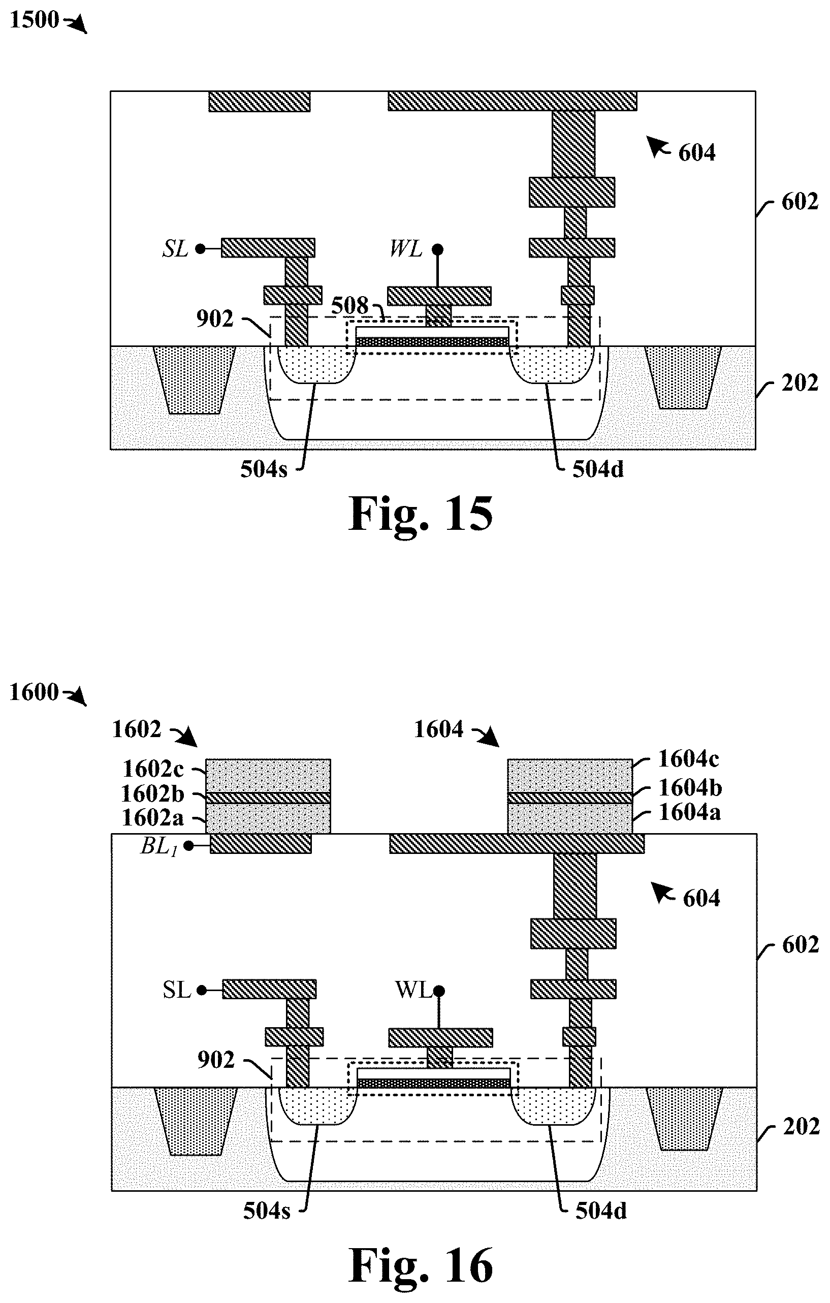
[0028] In some embodiments, the first conductive path and the second conductive path may comprise a same path 212. In other embodiments, the first conductive path may be a subset of the second conductive path. The first and second conductive paths may comprise a conductive wire (extending parallel to an upper surface of the substrate 202) and a conductive via (extending perpendicular to the upper surface of the substrate 202).
[0029] FIGS. 3A-3D illustrate some embodiments of schematic diagrams showing operation of a disclosed memory circuit.
[0030] FIG. 3A illustrates a schematic diagram 300 of an example of a first write operation to write a high data state to a target memory device 102 and a low data state to a complementary memory device 104.
[0031] The first write operation is performed by applying a first non-zero word-line voltage V.sub.WL1 to the word-line WL, a first non-zero bit-line voltage V.sub.BL1 to the bit-line BL, and a substantially zero source-line voltage V.sub.SL0 to the source-line SL. The first non-zero word-line voltage V.sub.WL1 turns on the control device 106 to form a conductive path between the source-line SL and the target memory device 102 and between the source-line SL and the complementary memory device 104.
[0032] The first non-zero bit-line voltage V.sub.BL1 and the substantially zero source-line voltage V.sub.SL0 form a first potential difference between a lower electrode LE.sub.1 and an upper electrode UE.sub.1 of the target memory device 102. The first potential difference causes a high data state (e.g., a `1`) to be written to the target memory device 102. The first non-zero bit-line voltage V.sub.BL1 and the substantially zero source-line voltage V.sub.SL0 also form a second potential difference between a lower electrode LE.sub.2 and an upper electrode UE.sub.2 of the complementary memory device 104, which has an opposite sign as the first potential difference. The second potential difference causes a low data state (e.g., a `0`) to be written to the complementary memory device 104.
[0033] FIG. 3B illustrates a schematic diagram 302 of an example of a second write operation to write a low data state to a target memory device 102 and a high data state to a complementary memory device 104.
[0034] The second write operation is performed by applying a second non-zero word-line voltage V.sub.WL2 to the word-line WL, a substantially zero bit-line voltage V.sub.BL0 to the bit-line BL, and a first non-zero source-line voltage V.sub.SL1 to the source-line SL. The second non-zero word-line voltage V.sub.WL2 turns on the control device 106 to form a conductive path between the source-line SL and the target memory device 102 and between the source-line SL and the complementary memory device 104.
[0035] The substantially zero bit-line voltage V.sub.BL0 and the first non-zero source-line voltage V.sub.SL1 form a first potential different between the lower electrode LE.sub.1 and the upper electrode UE.sub.1 of the target memory device 102. The first potential difference writes a low data state (e.g., a `0`) to the target memory device 102. The substantially zero bit-line voltage V.sub.BL0 and the first non-zero source-line V.sub.SL1 voltage also form a second potential different between the lower electrode LE.sub.2 and the upper electrode UE.sub.2 of the complementary memory device 104, which has an opposite sign as the first potential difference. The second potential difference causes a high data state (e.g., a `1`) to be written to the complementary memory device 104.
[0036] FIGS. 3C-3D illustrate schematic diagrams, 304 and 306, of exemplary read operations to read a data state from a target memory device. It will be appreciated that in the read operations shown in FIGS. 3C-3D, the described bias conditions allow for data to be read from the target memory device 102 along the bit-lines. However, in some alternative embodiments, data may be read from the target memory device along the source-lines. In such embodiments, a non-zero bias voltage is applied to the source-line SL.
[0037] In some embodiments, a read operation may be performed by applying a third non-zero word-line voltage V.sub.WL3 to the word-line WL and a second non-zero bit-line voltage V.sub.BL2 to the bit-line BL. The second non-zero word-line voltage V.sub.WL2 turns on the control device 106 to form a conductive path between the source-line SL and the target memory device 102 and between the source-line SL and the complementary memory device 104.
[0038] As shown in schematic diagram 304 of FIG. 3C, if the target memory device 102 is storing a high data state, the charges stored in the target memory device 102 will cause a first current I.sub.T to be provided to a first input 108a of a sense amplifier 108 by way of a target bit-line BL.sub.T, and a second current I.sub.C<I.sub.T to be provided to a second input 108b of the sense amplifier 108 by way of a complementary bit-line BL.sub.C. The sense amplifier 108 is configured to compare the first current I.sub.T to the second current I.sub.C and based upon the comparison to output a signal corresponding to a high data state (e.g., a `1`).
[0039] As shown in schematic diagram 306 of FIG. 3D, if the target memory device 102 is storing a low data state, the charges stored in the target memory device 102 will cause a first current I.sub.T to be provided to the first input 108a of the sense amplifier 108 by way of the target bit-line BL.sub.T, and a second current I.sub.C>I.sub.T to be provided to the second input 108b of the sense amplifier 108 by way of the complementary bit-line BL.sub.C. The sense amplifier 108 is configured to compare the first current I.sub.T to the second current I.sub.C and based upon the comparison to output a signal corresponding to a low data state (e.g., a `0`).
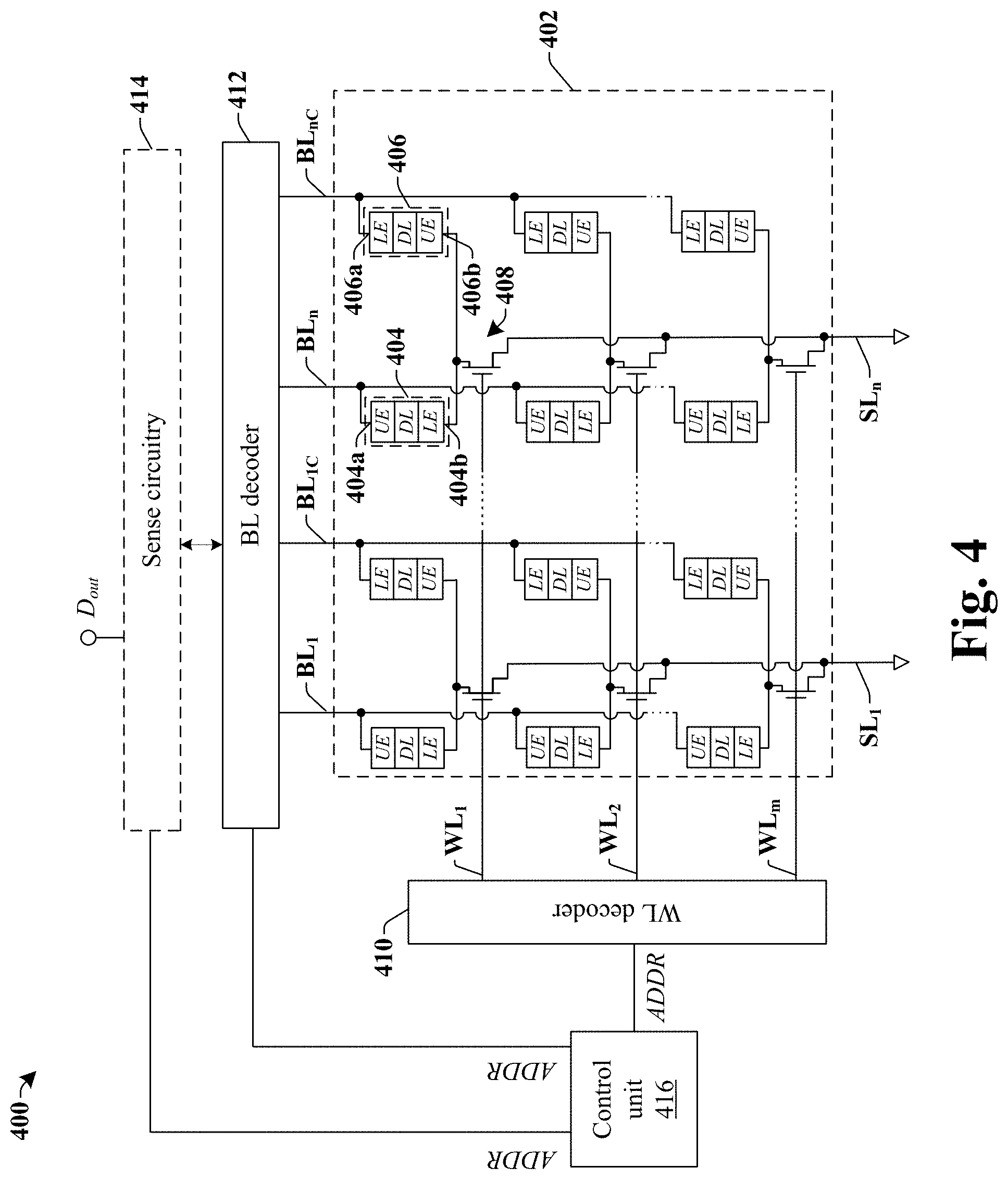
[0040] FIG. 4 illustrates a schematic diagram of some embodiments of a memory circuit 400 having shared transistors configured to provide access to target and complementary memory devices.
[0041] The memory circuit 400 comprises a memory array 402 having a plurality of target memory devices 404 (e.g., corresponding to target memory devices 102) and a plurality of complementary memory devices 406 (e.g., corresponding to complementary memory devices 104). The target memory devices 404 and the complementary memory devices 406 are arranged within the memory array 402 in rows and/or columns. Target memory devices 404 and complementary memory devices 406 within a row are operably coupled to a word-line WL.sub.1-WL.sub.m. Target memory devices 404 within a column are operably coupled to a bit-line BL.sub.1-BL.sub.n and a source-line SL.sub.1-SL.sub.n, while complementary memory devices 406 within a column are operably coupled to a complementary bit-line BL.sub.1C-BL.sub.nC and a source-line SL.sub.1-SL.sub.n.
[0042] Access transistors 408 are coupled to the target memory devices 404 and to the complementary memory devices 406. In some embodiments, the target memory devices 404 have a first terminal 404a coupling an upper electrode to a bit-line BL.sub.1-BL.sub.n and a second terminal 404b coupling a lower electrode to a first terminal of the access transistor 408. The complementary memory devices 406 also have a first terminal 406a coupling a lower electrode to a complementary bit-line BL.sub.1C-BL.sub.nC and a second terminal coupling an upper electrode to the first terminal of the access transistor 408. The access transistor 408 further has a gate coupled to a word-line WL.sub.1-WL.sub.m and a source coupled to a source-line SL.sub.1-SL.sub.n.
[0043] The memory array 402 is coupled to support circuitry that is configured to read data from and/or write data to the target memory devices 404 and to the complementary memory devices 406. In some embodiments, the support circuitry comprises a word-line decoder 410, a bit-line decoder 412, sensing circuitry 414 comprising one or more sense amplifiers, and a control unit 416. The word-line decoder 410 is configured to selectively apply a signal (e.g., a current and/or voltage) to one of the word-lines WL.sub.1-WL.sub.2, and the bit-line decoder 412 is configured to selectively apply a signal to one of the plurality of bit-lines BL.sub.1-BL.sub.2 based upon an address ADDR received from the control unit 416. By selectively applying signals to the word-lines WL.sub.1-WL.sub.2, the bit-lines BL.sub.1-BL.sub.2, the support circuitry is able to perform forming, set, reset, and read operations on selected ones of the target memory devices 404 and/or the complementary memory devices 406, as described above.
[0044] FIGS. 5-6 illustrate cross-sectional views of some embodiments of memory circuits having a target RRAM device (e.g., corresponding to 102) and a complementary RRAM device (e.g., corresponding to 104) coupled to a shared access transistor (e.g., corresponding to 204). It will be appreciated that the RRAM circuits, 500 and 600, shown in FIGS. 5-6 are non-limiting examples of RRAM circuits that have a shared access transistor, and that in other embodiments RRAM circuits may have different architectures while still having a shared access transistor.
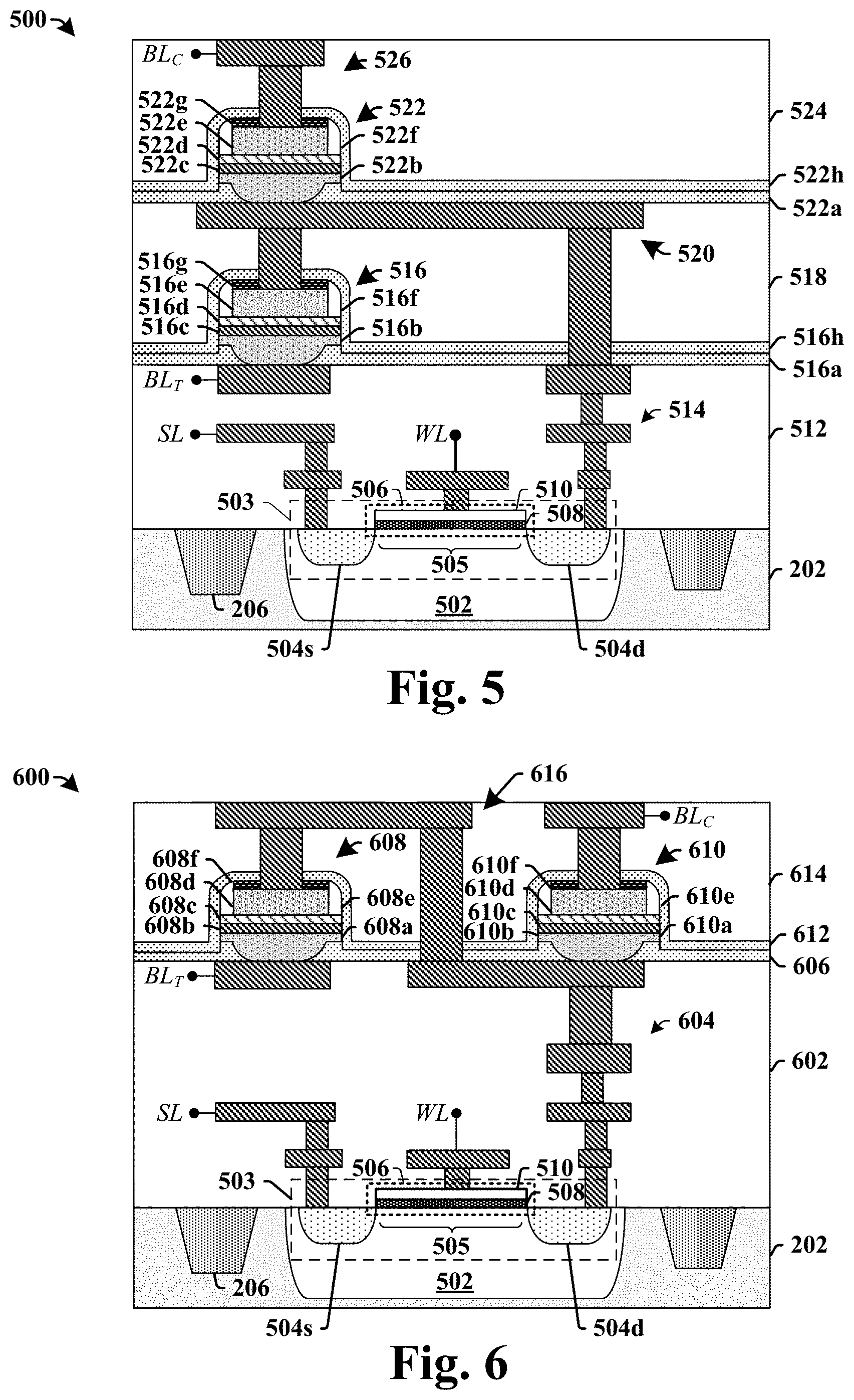
[0045] FIG. 5 illustrates a cross-sectional view of some embodiments of an RRAM circuit 500 having a shared transistor for access to target and complementary RRAM devices.
[0046] The RRAM circuit 500 comprises an access transistor 503 disposed within a substrate 202. In some embodiments, the access transistor 503 may be arranged within a well region 502. The access transistor 503 comprises a source region 504s, a drain region 504d separated from the source region 504s by a channel region 505, and a gate structure 506 arranged over the channel region 505. The gate structure 506 comprises a gate electrode 510 separated from the channel region 505 by a gate dielectric layer 508.
[0047] A first inter-level dielectric (ILD) structure 512 is arranged over the substrate 202. In some embodiments, the first ILD structure 512 may comprise one or more stacked dielectric layers (e.g., an oxide layer, a low-k dielectric layer, and/or an ultra low-k dielectric layer). The one or more stacked dielectric layers may be separated from one another by an etch stop layer (not shown). A first plurality of interconnect layers 514 (e.g., contact, wire, and via layers) are surrounded by the first ILD structure 512. In some embodiments, the first plurality of interconnect layers 514 may comprise copper, tungsten, and/or aluminum. The first plurality of interconnect layers 514 are configured to couple the source region 504s to a source-line SL and the gate electrode 510 to a word-line WL. In some embodiments, the source-line SL may be arranged on a second metal wire layer and the word-line WL may be arranged on the first metal wire layer.
[0048] A target RRAM device 516 is arranged within a second ILD structure 518 over the first ILD structure 512. The target RRAM device 516 comprises a lower electrode 516b, a data storage structure 516c having a variable resistance, and an upper electrode 516e. In some embodiments, the target RRAM device 516 may further comprise a lower insulating layer 516a surrounding a bottom part of the lower electrode 516b, a capping layer 516d between the data storage structure 516c and the upper electrode 516e, sidewall spacers 516f on opposing sides of the upper electrode 516e, a masking layer 516g over the upper electrode 516e, and/or an upper insulating layer 516h over the masking layer 516g. The lower electrode 516b is coupled to a target bit-line BL.sub.T by one or more of the first plurality of interconnect layers 514. In some embodiments, the target bit-line BL.sub.T may be arranged on a third metal wire layer. A second ILD structure 518 is disposed over target RRAM device 516, and a second plurality of interconnect layers 520 are arranged within the second ILD structure 518. The second plurality of interconnect layers 520 are configured to couple the upper electrode 516e of the target RRAM device 516 to the drain region 504d by way of the first plurality of interconnect layers 514.
[0049] In some embodiments, the lower electrode 516b and the upper electrode 516e may comprise a metal, such as tantalum (Ta) and/or titanium (Ti). In some embodiments, the data storage structure 516c may comprise a high-k dielectric material, such as titanium aluminum oxide, hafnium tantalum oxide, zirconium lanthanum oxide, or other suitable materials. In some embodiments, the capping layer 516d may comprise a metal (e.g., such as titanium (Ti), hafnium (Hf), platinum (Pt), aluminum (Al)) or a metal oxide (e.g., such as titanium oxide (TiO), hafnium oxide (HfO), zirconium oxide (ZrO), germanium oxide (GeO), cesium oxide (CeO)), or other suitable materials. In some embodiments, the masking layer 516g may comprise a silicon oxy-nitride (SiON) hard mask layer, a silicon dioxide (SiO.sub.2) hard mask layer, a PE-SiN hard mask, or other suitable materials.
[0050] A complementary RRAM device 522 is arranged within a third ILD structure 524 over the second ILD structure 518. The complementary RRAM device 522 comprises a lower electrode 522b, a data storage structure 522c arranged over the lower electrode 522b, and an upper electrode 522e arranged over the data storage structure 522c. In some embodiments, the complementary RRAM device 522 may also comprise a lower insulating layer 522a surrounding a bottom part of the lower electrode 522b, a capping layer 522d arranged between the data storage structure 522c and the upper electrode 522e, sidewall spacers 522f disposed on opposing sides of the upper electrode 522e, a masking layer 522g disposed over the upper electrode 522e, and/or an upper insulating layer 522h may be arranged over the masking layer 522g.
[0051] The second plurality of interconnect layers 520 are configured to couple the lower electrode 522b of the complementary RRAM device 522 to the drain region 504d by way of the first plurality of interconnect layers 514. In some embodiments, the second plurality of interconnect layers 520 may comprise a metal wire that extends between the upper electrode 516e and the lower electrode 522b. A third ILD structure 524 is arranged over the complementary RRAM device 522. The third ILD structure 524 surrounds a third plurality of interconnect layers 526 configured to couple the upper electrode 522e of a complementary bit-line BL.sub.C. In some embodiments, the third ILD structure 524 may comprise an ILD layer (e.g., having a single dielectric material) separated from the second ILD structure 518 by an etch stop layer. In some embodiments, the complementary bit-line BL.sub.C may be arranged on a fifth metal wire layer.
[0052] The target RRAM device 516 and the complementary RRAM device 522 are arranged at different heights with respect to the substrate 202. For example, the target RRAM device 516 has a bottommost surface that is closer to the substrate 202 than a bottommost surface of the complementary RRAM device 522. In some embodiments, the complementary RRAM device 522 may be arranged directly above the target RRAM device 516. In some embodiments, the complementary RRAM device 522 may be arranged directly above the access transistor 503. In some embodiments, the complementary RRAM device 522 and the target RRAM device 516 may be laterally offset from one another, but arranged above a memory cell region between isolation regions 206 within the substrate 202. Having the target RRAM device 516 and the complementary RRAM device 522 on different vertical positions allows for the memory cell to achieve a small footprint.
[0053] FIG. 6 illustrates a cross-sectional view of some alternative embodiments of a RRAM circuit 600 having a shared transistor for access to target and complementary RRAM cells.
[0054] The RRAM circuit 600 comprises an access transistor 503 arranged within a substrate 202 and having a source region 504s, a drain region 504d, and a gate structure 506. A first ILD structure 602 is arranged over the substrate 202. In some embodiments, a first plurality of interconnect layers 604 are surrounded by the first ILD structure 602. The first plurality of interconnect layers 604 are configured to couple the source region 504s to a source-line SL and the gate electrode 510 to a word-line WL.
[0055] A second ILD structure 614 is over the first ILD structure 602 and surrounds a target RRAM device 608, a complementary RRAM device 610, and a second plurality of interconnect layers 616. A horizontal plane extending parallel to a top surface of the substrate 202 extends through the target RRAM device 608 and the complementary RRAM device 610. In some embodiments, the second ILD structure 614 may comprise an ILD layer (e.g., having a single dielectric material) separated from the first ILD structure 602 by an etch stop layer.
[0056] The target RRAM device 608 comprises a lower electrode 608a, a data storage structure 608b having a variable resistance, and an upper electrode 608d arranged over the data storage structure 608b. In some embodiments, the target RRAM device 608 may further comprise a capping layer 608c arranged between the data storage structure 608b and the upper electrode 608d, sidewall spacers 608e disposed on opposing sides of the upper electrode 608d, and/or a masking layer 608f disposed over the upper electrode 608d. The lower electrode 608a is coupled to a target bit-line BL.sub.T by way of the first plurality of interconnect layers 604. The upper electrode 608d is coupled to the drain region 504d by way of the first plurality of interconnect layers 604 and the second plurality of interconnect layers 616.
[0057] The complementary RRAM device 610 comprises a lower electrode 610a, a data storage structure 610b arranged over the lower electrode 610a, and an upper electrode 610d arranged over the data storage structure 610b. In some embodiments, the complementary RRAM device 610 comprises may further comprise a capping layer 610c arranged between the data storage structure 610b and the upper electrode 610d, sidewall spacers 610e disposed on opposing sides of the upper electrode 610d, and/or a masking layer 610f disposed over the upper electrode 610d. In some embodiments, the target RRAM device 608 and the complementary RRAM device 610 are arranged over a lower insulating layer 606 and are covered by an upper insulating layer 612. The lower electrode 608a is coupled to the drain region 504d by way of the first plurality of interconnect layers 604. The upper electrode 608d is coupled to a complementary bit-line BL.sub.C by way of the second plurality of interconnect layers 616.
[0058] It will be appreciated that although RRAM circuits 500 and 600 are described as having complementary and target RRAM devices at certain locations, that in other embodiments the locations of the complementary and target RRAM devices may be switched. For example, in some embodiments, a target RRAM device may be above a complementary RRAM device.
[0059] FIG. 7 illustrates a table 700 showing some embodiments of operating conditions of an RRAM circuit having a shared transistor for access to target and complementary RRAM devices. The table 700 comprises a first column 702 describing exemplary bias conditions to set a target RRAM device to a high data state (e.g., corresponding to a logical `1`) and to reset a complimentary RRAM device to a low data state (e.g., corresponding to a logical `0`), a second column 704 describing exemplary bias conditions to reset a target RRAM device to a low data state and to set a complimentary RRAM device to a high data state, and a third column 706 describing exemplary bias conditions to read data from a target RRAM device.
[0060] FIGS. 8A-8C illustrate flow diagrams of some embodiments of methods of operating an RRAM circuit having a shared transistor for access to target and complementary memory devices. It will be appreciated that in some non-limiting embodiments, the methods of operating an RRAM circuit may be applied to the RRAM circuits, 500 and/or 600, of FIGS. 5-6.
[0061] FIG. 8A illustrates a flow diagram of some embodiments of a method 800 of writing a high data state to a RRAM memory cell within a memory circuit having a shared control device configured to provide access to target and complementary memory devices. Column 702 of table 700 illustrates some examples of bias conditions corresponding to acts 802-806 of method 800.
[0062] At 802, a non-zero word-line voltage is applied to a gate of an access transistor having a first source/drain terminal coupled to a lower electrode of a target device and an upper electrode of a complementary device.
[0063] At 804, a non-zero bit-line voltage is concurrently applied to an upper electrode of the target device and a lower electrode of the complementary device.
[0064] At 806, a substantially zero source-line voltage is applied to a second source/drain terminal of the access transistor. The substantially zero source-line voltage causes the lower electrode of the target device to be held at a low voltage potential, which drives the target device to a high data state. The substantially zero source-line voltage also causes the upper electrode of the complementary device to be held at a low voltage potential, which drives the complementary device to a low data state.
[0065] FIG. 8B illustrates a flow diagram of some embodiments of a method 808 of writing a low data state to a target memory device of a memory circuit having a shared control device for access to target and complementary memory devices. Column 704 of table 700 illustrates some examples of bias conditions corresponding to acts 810-814 of method 808.
[0066] At 810, a non-zero word-line voltage is applied to a gate of an access transistor having a first source/drain terminal coupled to a lower electrode of a target device and an upper electrode of a complementary device.
[0067] At 812, a substantially zero bit-line voltage is concurrently applied to an upper electrode of the target device and a lower electrode of the complementary device.
[0068] At 814, a non-zero source-line voltage is applied to a second source/drain terminal of the access transistor. The non-zero source-line voltage causes the lower electrode of the target device to be held at a high voltage potential, which drives the target device to a low data state. The non-zero source-line voltage also causes the upper electrode of the complementary device to be held at a high voltage potential, which drives the complementary device to a high data state.
[0069] FIG. 8C illustrates a flow diagram of some embodiments of a method 816 of reading a data state from a target memory device of a memory circuit having a shared control device for access to target and complementary memory devices. Column 706 of table 700 illustrates some examples of bias conditions corresponding to acts 818-822 of method 816.
[0070] At 818, a non-zero word-line voltage is applied to a gate of an access transistor having a first source/drain terminal coupled to a lower electrode of a target device and an upper electrode of a complementary device.
[0071] At 820, a non-zero bit-line voltage is concurrently applied to an upper electrode of the target device and a lower electrode of the complementary device.
[0072] At 822, a substantially zero source-line voltage is applied to a second source/drain terminal of the access transistor.
[0073] FIGS. 9-13 illustrate cross-sectional views 900-1300 of some embodiments of a method of forming an integrated chip comprising a memory circuit having a shared transistor for access to both target and complementary devices. Although FIGS. 9-13 are described in relation to a method, it will be appreciated that the structures disclosed in FIGS. 9-13 are not limited to such a method, but instead may stand alone as structures independent of the method.
[0074] As shown in cross-sectional view 900 of FIG. 9, a control device 902 is formed within a substrate 202. In some embodiments, the control device 902 may comprise a transistor device. For example, in various embodiments, the control device 902 may comprise a MOSFET, a bi-polar junction transistor (BJT), a high electron mobility transistor (HEMT), or a similar device. In various embodiments, the substrate 202 may be any type of semiconductor body (e.g., silicon, SiGe, SOI, etc.), such as a semiconductor wafer and/or one or more die on a wafer, as well as any other type of semiconductor and/or epitaxial layers, associated therewith.
[0075] In some embodiments, the control device 902 may comprise a transistor formed by depositing a gate dielectric film and a gate electrode film over the substrate 202. The gate dielectric film and the gate electrode film are subsequently patterned to form a gate dielectric layer 508 and a gate electrode 510. The substrate may be subsequently implanted to form a source region 504s and a drain region 504d within the substrate 202 on opposing sides of the gate structure 506.
[0076] As shown in cross-sectional view 1000 of FIG. 10, a first plurality of interconnect layers 514 are formed within a first ILD structure 512 over the substrate 202. The first plurality of interconnect layers 514 couple the source region to a source-line SL and the gate structure 506 to a word-line WL. The first plurality of interconnect layers 514 may be formed by repeatedly depositing an ILD layer over the substrate, selectively etching the ILD layer (e.g., an oxide, a low-k dielectric, or an ultra low-k dielectric) to define a via hole and/or a trench within the ILD layer, forming a conductive material (e.g., copper, aluminum, etc.) within the via hole and/or a trench to fill the opening, and performing a planarization process (e.g., a chemical mechanical planarization process).
[0077] As shown in cross-sectional view 1100 of FIG. 11, a first memory device 1102 is formed over the first ILD structure 512. The first memory device 1102 comprises a first lower electrode 1102a separated from a first upper electrode 1102c by way of a first data storage layer 1102b. In various embodiments, the first memory device 1102 may comprise an RRAM device, a PCRAM device, an MRAM device, a DRAM device, a CBRAM device, or a CNT device, or the like. The first lower electrode 1102a is coupled to a first bit-line BL.sub.1 within the first plurality of interconnect layers 514.
[0078] In some embodiments, the first memory device 1102 may be formed by depositing a lower electrode film over the first ILD structure 512, forming a data storage element over the lower electrode film, and forming an upper electrode film over the data storage element. In some embodiments, the lower and upper electrode films may comprise a conductive materials formed by way of a deposition technique (e.g., physical vapor deposition (PVD), chemical vapor deposition (CVD), PE-CVD, atomic layer deposition (ALD), sputtering, etc.) and the data storage element may comprise a dielectric material formed by way of a deposition technique. For example, the lower and upper electrode films may comprise a metal or metal alloy comprising titanium (Ti) and/or tantalum (Ta), while the data storage element may comprise a high-k dielectric material (e.g., hafnium oxide). One or more patterning processes are performed on the upper electrode film to define the first upper electrode 1102c, the data storage element to define the first data storage layer 1102b, and the lower electrode film to define the first lower electrode 1102a. In some embodiments, the one or more patterning processes may use a dry etchant having an etching chemistry comprising a fluorine species (e.g., CF.sub.4, CHF.sub.3, C.sub.4F.sub.8, etc.) or a wet etchant comprising hydrofluoric acid (HF).
[0079] As shown in cross-sectional view 1200 of FIG. 12, a second ILD structure 518 is formed over the first memory device 1102. The second ILD structure 518 may be formed by one or more deposition processes (e.g., PVD, CVD, PE-CVD, etc.). A second plurality of interconnect layers 520 are formed within the second ILD structure 518. The second plurality of interconnect layers 520 couple the first upper electrode 1102c to the drain region 504d by way of the first plurality of interconnect layers 514. In some embodiments, the second plurality of interconnect layers 520 may be formed by selectively etching the second ILD structure 518 to form openings within the second ILD structure 518. A conductive material (e.g., copper and/or aluminum) is then deposited within the openings.
[0080] As shown in cross-sectional view 1300 of FIG. 13, a second memory device 1302 is formed over the second ILD structure 518. The second memory device 1302 comprises a second lower electrode 1302a separated from a second upper electrode 1302c by way of a second data storage layer 1302b. The second lower electrode 1302a may be coupled to the drain region 504d by way of the first plurality of interconnect layers 514 and the second plurality of interconnect layers 520. In some embodiments, the second memory device 1302 may be formed by a process similar to the process used to form the first memory device 1102.
[0081] A third ILD structure 524 is formed over the second memory device 1302, and a third plurality of interconnect layers 526 is subsequently formed within the third ILD structure 524. The second upper electrode 1302c is coupled to a second bit-line BL.sub.2 within the third plurality of interconnect layers 526.
[0082] FIGS. 14-17 illustrate cross-sectional views 1400-1700 of some alternative embodiments of a method of forming an integrated chip comprising a memory circuit having a shared transistor for access to target and complementary devices. Although FIGS. 14-17 are described in relation to a method, it will be appreciated that the structures disclosed in FIGS. 14-17 are not limited to such a method, but instead may stand alone as structures independent of the method.
[0083] As shown in cross-sectional view 1400 of FIG. 14, a control device 902 is formed within a substrate 202. In various embodiments, the control device 902 may comprise a transistor device, such as a MOSFET, a BJT, a HEMT, or a similar device.
[0084] As shown in cross-sectional view 1500 of FIG. 15, a first plurality of interconnect layers 604 are formed within a first ILD structure 602 over the substrate 202. The first plurality of interconnect layers 604 are configured to couple a source region 504s of the control device 902 to a source-line SL and a drain region 504d of the control device 902 to a word-line WL.
[0085] As shown in cross-sectional view 1600 of FIG. 16, a first memory device 1602 and a second memory device 1604 are formed over a first ILD structure 602. The first memory device 1602 comprises a first lower electrode 1602a separated from a first upper electrode 1602c by way of a first data storage layer 1602b. The second memory device 1604 comprises a second lower electrode 1604a separated from a second upper electrode 1604c by way of a second data storage layer 1604b. The first plurality of interconnect layers 604 are configured to couple the first lower electrode 1602a to a first bit-line BL.sub.1 and the second lower electrode to source region of the control device 902.
[0086] As shown in cross-sectional view 1700 of FIG. 17, a second ILD structure 614 is formed over the first memory device 1602 and the second memory device 1604. The second ILD structure 614 may be formed by a deposition process (e.g., PVD, CVD, PE-CVD, etc.) to cover the first memory device 1602 and the second memory device 1604. A second plurality of interconnect layers 616 are formed within the second ILD structure 614. The second plurality of interconnect layers 616 are configured to couple the first upper electrode 1602c to the source region of the control device 902 and to further couple the second upper electrode 1604c to a second bit-line BL.sub.2.
[0087] FIG. 18 illustrates a flow diagram of some embodiments of a method 1800 of forming an integrated chip comprising an RRAM device having a multi-layer data storage structure.
[0088] While method 1800 is illustrated and described below as a series of acts or events, it will be appreciated that the illustrated ordering of such acts or events are not to be interpreted in a limiting sense. For example, some acts may occur in different orders and/or concurrently with other acts or events apart from those illustrated and/or described herein. In addition, not all illustrated acts may be required to implement one or more aspects or embodiments of the description herein. Further, one or more of the acts depicted herein may be carried out in one or more separate acts and/or phases.
[0089] At 1802, a control device is formed within a substrate. The control device comprises a first terminal, a second terminal, and a third terminal. In some embodiments, the first terminal may comprise a source region, the second terminal may comprise a gate structure, and the third terminal may comprise a drain region. FIG. 9 illustrates a cross-sectional view 900 of some embodiments corresponding to act 1802. FIG. 14 illustrates a cross-sectional view 1400 of some alternative embodiments corresponding to act 1802.
[0090] At 1804, a first plurality of interconnect layers are formed within a first ILD structure over the substrate. The first plurality of interconnect layers couple the first terminal to a source-line and the second terminal to a word-line. FIG. 10 illustrates a cross-sectional view 1000 of some embodiments corresponding to act 1804. FIG. 15 illustrates a cross-sectional view 1500 of some alternative embodiments corresponding to act 1804.
[0091] At 1806, a first memory device is formed. The first memory device has a first lower electrode coupled to a first bit-line and a first upper electrode coupled to the third terminal by way of a first conductive path comprising the first plurality of interconnect layers. FIG. 12 illustrates a cross-sectional view 1200 of some embodiments corresponding to act 1806. FIG. 16 illustrates a cross-sectional view 1600 of some embodiments corresponding to act 1806.
[0092] At 1808, a second memory element is formed. The second memory device has a second lower electrode coupled to the third terminal by way of a second conductive path comprising the first plurality of interconnect layers and a second upper electrode coupled to the second bit-line. FIG. 13 illustrate a cross-sectional view 1300 of some embodiments corresponding to act 1808. FIGS. 16-17 illustrate cross-sectional views 1600-1700 of some embodiments corresponding to act 1808.
[0093] Therefore, the present disclosure in various embodiments relates to a memory circuit having a shared control device for access to both target and complementary memory devices of a memory array configured to operate using differential sensing.
[0094] In some embodiments, the present disclosure relates to a memory circuit. The memory circuit includes a control device arranged within a substrate and having a first terminal coupled to a source-line, a second terminal coupled to a word-line, and a third terminal; a first memory device having a first lower electrode separated from a first upper electrode by a first data storage layer, the first upper electrode is coupled to the third terminal and the first lower electrode is coupled to a first bit-line; and a second memory device having a second lower electrode separated from a second upper electrode by a second data storage layer, the second upper electrode is coupled to a second bit-line and the second lower electrode is coupled to the third terminal. In some embodiments, the control device comprises a transistor device having a source region coupled to the source-line, a gate structure coupled to the word-line, and a drain region coupled to the first upper electrode and the second lower electrode. In some embodiments, the first memory device and the second memory device are resistive random access memory (RRAM) devices. In some embodiments, the circuit further includes a first inter-level dielectric (ILD) structure between the first memory device and the substrate; a second ILD structure over the first ILD structure and surrounding the first memory device; and a third ILD structure over the second ILD structure and surrounding the second memory device. In some embodiments, the circuit further includes a first plurality of interconnect layers arranged within the first ILD structure and a second plurality of interconnect layers arranged within the second ILD structure, the second plurality of interconnect layers comprise a metal wire extending between the first upper electrode and the second lower electrode and coupled to the second terminal by way of the first plurality of interconnect layers. In some embodiments, the second memory device is arranged directly above the first memory device. In some embodiments, the second ILD structure is separated from the third ILD structure by an etch stop layer. In some embodiments, the first memory device has a bottommost surface that is closer to the substrate than a bottommost surface of the second memory device. In some embodiments, a horizontal plane extending parallel to an upper surface of the substrate extends through the first memory device and the second memory device. In some embodiments, the first bit-line is selectively configured to be coupled to a first input of a sense amplifier concurrent to the second bit-line being coupled to a second input of the sense amplifier. In some embodiments, the first memory device is configured to concurrently store a data state that is different than the second memory device.
[0095] In other embodiments, the present disclosure relates to a memory circuit. The memory circuit includes a control device arranged within a substrate; a first memory device arranged within a dielectric structure over the substrate and having a first lower electrode separated from a first upper electrode by a first data storage layer; a plurality of interconnect layers surrounded by the dielectric structure and configured to couple the first upper electrode to the control device and the first lower electrode to a first bit-line; and a second memory device arranged within the dielectric structure and having a second lower electrode separated from a second upper electrode by a second data storage layer, the plurality of interconnect layers are configured to couple the second upper electrode to a second bit-line and the second lower electrode to the control device. In some embodiments, the plurality of interconnect layers comprise a conductive path that continuously extends between the first upper electrode and the second lower electrode. In some embodiments, the conductive path comprises a conductive wire and a conductive via. In some embodiments, the control device has a first terminal coupled to a source-line, a second terminal coupled to a word-line, and a third terminal coupled to the first upper electrode and the second lower electrode. In some embodiments, the circuit further includes a first inter-level dielectric (ILD) structure over the substrate; a second ILD structure over the first ILD structure and surrounding the first memory device; and a third ILD structure over the second ILD structure and surrounding the second memory device. In some embodiments, the control device is arranged within a memory cell region surrounded by one or more isolation regions within the substrate; and the first memory device and the second memory device are arranged directly over the memory cell region.
[0096] In yet other embodiments, the present disclosure relates to a method of forming a memory circuit. The method includes forming a control device within a substrate; forming a first memory device having a first lower electrode coupled to a first bit-line and a first upper electrode coupled to the control device; and forming a second memory device having a second lower electrode coupled to the control device and a second upper electrode coupled to a second bit-line. In some embodiments, the first memory device has a bottommost surface that is closer to the substrate than a bottommost surface of the second memory device. In some embodiments, a horizontal plane extending parallel to an upper surface of the substrate extends through the first memory device and the second memory device.
[0097] In yet other embodiments, the present disclosure relates to a method of forming a memory circuit. The method includes forming a control device within a substrate; forming a first ILD structure over the substrate, the first ILD structure comprises a first plurality of interconnect layers; forming a first memory device over the first ILD structure, the first memory device has a first lower electrode coupled to a first bit-line and a first upper electrode coupled to the control device by way of a first conductive path comprising the first plurality of interconnect layers; and forming a second memory device over the first ILD structure, the second memory device has a second lower electrode coupled to the control device by way of a second conductive path comprising the first plurality of interconnect layers and a second upper electrode coupled to a second bit-line. In some embodiments, the method further includes forming a second ILD structure surrounding the first memory device and a second plurality of interconnect layers, the second plurality of interconnect layers couple the first upper electrode to the control device by way of the first plurality of interconnect layers. In some embodiments, the second plurality of interconnect layers comprise a metal wire extending between the first memory device and the second memory device. In some embodiments, the second ILD structure further surrounds the second memory device and couples the second upper electrode coupled to the second bit-line. In some embodiments, the method further includes forming a third ILD structure surrounding a third plurality of interconnect layers over the second memory device, the third plurality of interconnect layers couple the second upper electrode to the second bit-line. In some embodiments, the method further includes forming the first memory device concurrent to the second memory device, the first memory device and the second memory device are laterally adjacent to one another. In some embodiments, the method further includes forming the first memory device before forming the second memory device, the first memory device has a bottommost surface that is closer to the substrate than a bottommost surface of the second memory device.
[0098] In yet other embodiments, the present disclosure relates to a method of forming a memory circuit. The method includes forming an access transistor within a substrate, the access transistor has a source region, a drain region, and a gate structure; forming a first ILD structure over the substrate; forming a first memory device over the first ILD structure, the first memory device has a first lower electrode separated from a first upper electrode by a first data storage layer; forming a second memory device over the first ILD structure, the second memory device has a second lower electrode separated from a second upper electrode by a second data storage layer; and the first upper electrode and the second lower electrode are coupled to the drain region. In some embodiments, the method further includes forming a first plurality of interconnect layers within the first ILD structure; and forming a second plurality of interconnect layers within a second ILD structure over the first ILD structure, the first plurality of interconnect layers and the second plurality of interconnect layers couple the first upper electrode to the drain region. In some embodiments, the second ILD structure surrounds the first memory device. In some embodiments, the second lower electrode is coupled to the drain region by way of a conductive path comprising the first plurality of interconnect layers. In some embodiments, the method further includes forming a third ILD structure surrounding the second memory device, the first plurality of interconnect layers and the second plurality of interconnect layers couple the second lower electrode to the drain region. In some embodiments, the method further includes forming the first memory device concurrent to the second memory device. In some embodiments, the method further includes forming the first memory device before forming the second memory device.
[0099] In yet other embodiments, the present disclosure relates to a memory circuit. The memory circuit include an access transistor arranged within a substrate and having a first terminal coupled to a source-line, a second terminal coupled to a word-line, and a third terminal; a first memory device having a first lower electrode separated from a first upper electrode by a first data storage layer, the first lower electrode is configured to be selectively coupled to a first input terminal of a sense amplifier and the first upper electrode is coupled to the third terminal; and a second memory device having a second lower electrode separated from a second upper electrode by a second data storage layer, the second lower electrode is coupled to the third terminal and the second upper electrode is configured to be selectively coupled to a second input terminal of the sense amplifier concurrent to the first lower electrode being coupled to the first input terminal of the sense amplifier. In some embodiments, the first memory device and the second memory device are RRAM (resistive random access memory) devices, PCRAM (phase change random access memory) devices, FRAM (ferroelectric random access memory) devices, MRAM (magneto-resistive random access memory) devices, CBRAM (conductive bridging random access memory) devices, or carbon nano-tube (CNT) memory devices. In some embodiments, the first memory device and the second memory device are arranged within a dielectric structure over the substrate. In some embodiments, the access transistor comprises a source region corresponding to the first terminal, a gate structure corresponding to the second terminal, and a drain region corresponding to the third terminal. In some embodiments, the second memory device is vertically separated from the first memory device by an interconnect wire extending parallel to an upper surface of the substrate. In some embodiments, the second memory device and the first memory device vertically overlie the access transistor.
[0100] The foregoing outlines features of several embodiments so that those skilled in the art may better understand the aspects of the present disclosure. Those skilled in the art should appreciate that they may readily use the present disclosure as a basis for designing or modifying other processes and structures for carrying out the same purposes and/or achieving the same advantages of the embodiments introduced herein. For example, although the disclosure describes the oxygen barrier layer as being within a multi-layer upper electrode, it will be appreciated that the oxygen barrier layer is not limited to the upper electrode. Rather, the oxygen barrier layer may also or alternatively be present in a multi-layer lower electrode.
[0101] Those skilled in the art should also realize that such equivalent constructions do not depart from the spirit and scope of the present disclosure, and that they may make various changes, substitutions, and alterations herein without departing from the spirit and scope of the present disclosure.
* * * * *
D00000
D00001
D00002
D00003
D00004
D00005
D00006
D00007
D00008
D00009
D00010
D00011
XML
uspto.report is an independent third-party trademark research tool that is not affiliated, endorsed, or sponsored by the United States Patent and Trademark Office (USPTO) or any other governmental organization. The information provided by uspto.report is based on publicly available data at the time of writing and is intended for informational purposes only.
While we strive to provide accurate and up-to-date information, we do not guarantee the accuracy, completeness, reliability, or suitability of the information displayed on this site. The use of this site is at your own risk. Any reliance you place on such information is therefore strictly at your own risk.
All official trademark data, including owner information, should be verified by visiting the official USPTO website at www.uspto.gov. This site is not intended to replace professional legal advice and should not be used as a substitute for consulting with a legal professional who is knowledgeable about trademark law.