Conditional Execution Specification Of Instructions Using Conditional Extension Slots In The Same Execute Packet In A Vliw Proce
Anderson; Timothy David ; et al.
U.S. patent application number 16/558569 was filed with the patent office on 2019-12-26 for conditional execution specification of instructions using conditional extension slots in the same execute packet in a vliw proce. The applicant listed for this patent is TEXAS INSTRUMENTS INCORPORATED. Invention is credited to Timothy David Anderson, Duc Quang Bui, Joseph Raymond Michael Zbiciak.
| Application Number | 20190391812 16/558569 |
| Document ID | / |
| Family ID | 58558123 |
| Filed Date | 2019-12-26 |


| United States Patent Application | 20190391812 |
| Kind Code | A1 |
| Anderson; Timothy David ; et al. | December 26, 2019 |
CONDITIONAL EXECUTION SPECIFICATION OF INSTRUCTIONS USING CONDITIONAL EXTENSION SLOTS IN THE SAME EXECUTE PACKET IN A VLIW PROCESSOR
Abstract
In one embodiment, a system includes a memory and a processor core. The processor core includes functional units and an instruction decode unit configured to determine whether an execute packet of instructions received by the processing core includes a first instruction that is designated for execution by a first functional unit of the functional units and a second instruction that is a condition code extension instruction that includes a plurality of sets of condition code bits, wherein each set of condition code bits corresponds to a different one of the functional units, and wherein the sets of condition code bits include a first set of condition code bits that corresponds to the first functional unit. When the execute packet includes the first and second instructions, the first functional unit is configured to execute the first instruction conditionally based upon the first set of condition code bits in the second instruction.
| Inventors: | Anderson; Timothy David; (University Park, TX) ; Bui; Duc Quang; (Grand Prairie, TX) ; Zbiciak; Joseph Raymond Michael; (San Jose, CA) | ||||||||||
| Applicant: |
|
||||||||||
|---|---|---|---|---|---|---|---|---|---|---|---|
| Family ID: | 58558123 | ||||||||||
| Appl. No.: | 16/558569 | ||||||||||
| Filed: | September 3, 2019 |
Related U.S. Patent Documents
| Application Number | Filing Date | Patent Number | ||
|---|---|---|---|---|
| 14920298 | Oct 22, 2015 | 10402199 | ||
| 16558569 | ||||
| Current U.S. Class: | 1/1 |
| Current CPC Class: | G06F 9/30145 20130101; G06F 9/3802 20130101; G06F 9/3891 20130101; G06F 9/30072 20130101; G06F 9/30185 20130101; G06F 9/3013 20130101; G06F 9/3822 20130101; G06F 9/3853 20130101; G06F 9/30076 20130101 |
| International Class: | G06F 9/38 20060101 G06F009/38; G06F 9/30 20060101 G06F009/30 |
Claims
1. A system comprising: a memory; and a processor core including: a plurality of functional units; and an instruction decode unit configured to determine whether an execute packet of instructions received by the processing core includes: a first instruction that is designated for execution by a first functional unit of the plurality of functional units; and a second instruction that is a condition code extension instruction that includes a plurality of sets of condition code bits, wherein each set of condition code bits corresponds to a different one of the plurality of functional units, and wherein the sets of condition code bits include a first set of condition code bits that corresponds to the first functional unit; wherein, when the execute packet includes both the first instruction and the second instruction, the first functional unit is configured to execute the first instruction conditionally based upon the first set of condition code bits in the second instruction.
2. The system of claim 1, wherein the processing core is configured to execute the instructions of the execute packet in parallel using the plurality of functional units.
3. The system of claim 1, wherein, when the first instruction includes a set of condition code bits and the execute packet includes both the first instruction and the second instruction, the condition code bits of the first instruction are overridden by the first set of condition code bits of the second instruction.
4. The system of claim 1, wherein all the instructions in the execute packet have the same size.
5. The system of claim 4, wherein the size is 32 bits.
6. The system of claim 1, wherein the second instruction includes, in addition to the sets of condition code bits, a field containing a value to identify the second instruction as the condition code extension instruction.
7. The system of claim 1, wherein the first set of condition code bits includes: a first subset of bits to indicate a predicate register; a second subset of bits to indicate a condition.
8. The system of claim 7, wherein the condition indicated by the second subset of bits is whether the predicate register is equal to or not equal to zero.
9. The system of claim 8, wherein the processor includes a register file that includes a plurality of predicate registers, and wherein each of the plurality of predicate registers can be indicated by the first subset of bits using a respective coding.
10. The system of claim 9, wherein the first subset of bits is three bits.
11. The system of claim 10, wherein, in addition to each coding used to indicate a respective one of the plurality of predicate registers, the first subset of bits is configured to use an additional coding to indicate unconditional execution.
12. The system of claim 11, wherein the second subset of bits is a single bit.
13. The system of claim 1, further comprising a hierarchical memory system that includes a level one (L1) cache and a level two (L2) cache, wherein the memory is at least part of the L1 cache.
14. The system of claim 13, wherein the L1 cache includes an L1 data cache and an L1 instruction cache, and the memory is the L1 instruction cache.
15. The system of claim 1, wherein the processor core includes: an instruction fetch unit configured to fetch a plurality of instructions from the memory; and an instruction dispatch unit configured to determined which of the plurality of instructions are to be executed by the processor core in parallel and to group the instructions that are to be executed by the processor core in parallel into the execute packet.
16. The system of claim 1, wherein the processor core includes a digital signal processor DSP core.
17. A method comprising: receiving an execute packet of instructions; determine whether the instructions of the execute packet include a first instruction that is designated for execution by a first functional unit of a plurality of functional units of a processor and a second instruction that is a condition code extension instruction that includes a plurality of sets of condition code bits, wherein each set of condition code bits corresponds to a different one of the plurality of functional units, and wherein the sets of condition code bits include a first set of condition code bits that corresponds to the first functional unit; and using the first functional unit to execute the first instruction conditionally based upon the first set of condition code bits in the second instruction when the execute packet includes both the first instruction and the second instruction.
18. The method of claim 17, wherein the first and second instructions have the same size.
19. The method of claim 17, wherein the first and second instructions are separate instructions within the execute packet.
Description
CROSS-REFERENCE TO RELATED APPLICATION(S)
[0001] This application is a continuation of U.S. patent application Ser. No. 14/920,298 filed on Oct. 22, 2015, which is incorporated herein by reference.
TECHNICAL FIELD
[0002] The technical field of this invention is digital data processing and more specifically conditional instruction execution controlled by another instruction.
BACKGROUND
[0003] This invention deals with conditional instruction execution. Conditional instruction execution is typically accomplished by determining the status of a data register and executing or not executing the instruction depending upon this status. It is known in the art to use a zero/non-zero determination for this conditional execution.
[0004] Conditional instruction execution can be advantageously employed instead of conditional branching. In deeply pipelined data processors taking a conditional branch typically results in later fetched instructions in the pipeline being no longer on the instruction path through the program. In the prior art these later fetched instructions are flushed and new instructions on the branch instruction path are fetched. This results in a delay during which the instructions on the new branch instruction path catch up to the point where instructions were flushed. This delay is called a pipeline hit. The amount this slows the data processor operation is dependent upon the pipeline depth and the frequency of taken conditional braches.
[0005] Conditional instruction execution does not involve a pipeline hit. The program instruction path is unchanged and no instructions need to be flushed. A typical program data path using conditional branches selects an alternative data processing operation based upon the condition. Then the two branches merge for additional processing. This program data path can be easily implemented using conditional instruction execution. The alternate data processing operations are made conditional on the same condition in opposite senses. Based upon the condition, one data processing operation is executed and the other is not executed. This performs the desired alternative operation. If the alternate braches are short, ideally one instruction, then the conditional execution instruction path could be shorter than the conditional branch instruction data path. For data processors that can perform more than one instruction at a time, such as a very long instruction word (VLIW) processor or a super-scalar processor, the alternate data processing operations may be scheduled during the same instruction cycle. In this case condition instruction execution typically takes the same number of instruction cycles as a conditional branch instruction path when the branch is taken. Accordingly, conditional instruction execution may be advantageous over conditional branch operations in many instances.
SUMMARY
[0006] Employing conditional execution may be advantageous as noted above. However, there are problems with this technique. It is believe advantageous to have more than on register that can control conditional operation. The instruction includes bits that specify a particular register from among the registers available to control conditional execution. The more registers available to control conditional execution the more bits are needed within each instruction to specify the particular register. This reduces the number of bits available to specify other instruction operations, known as opcode space.
[0007] It is known in the art to employ a special auxiliary instruction for the conditional execution bits. This is advantageous in a VLIW processor where every slot in an execute packet may not be used. Accordingly, specification of conditional execution conditions need not require additional instruction cycles.
[0008] Yet another factor may create a problem. A VILW processor typically includes plural functional unit that may operate in parallel. The bits needed to specify conditional operation for all these functional units may exceed the instruction length. A fixed instruction length is believed advantageous for coding/decoding purposes. Thus extending the length of the conditional execution auxiliary instruction is not advantageous. One embodiment of this invention provides two such conditional execution auxiliary instructions directed to disparate subsets of the plural functional units. Depending on the conditional execution desired, only one of the two conditional execution auxiliary instructions may be required for a particular execute packet.
[0009] Another embodiment of this invention employs only one of two possible register files for the condition registers. In a VLIW processor it may be advantageous to split the functional units into separate sets with corresponding register files. This limits the number of functional units that may simultaneously access the register files. In the preferred embodiment of this invention the functional units are divided into a scalar set which access scalar registers and a vector set which access vector registers. The data registers storing the conditions for both scalar and vector instructions are in the scalar data register file.
BRIEF DESCRIPTION OF THE DRAWINGS
[0010] These and other aspects of this invention are illustrated in the drawings, in which:
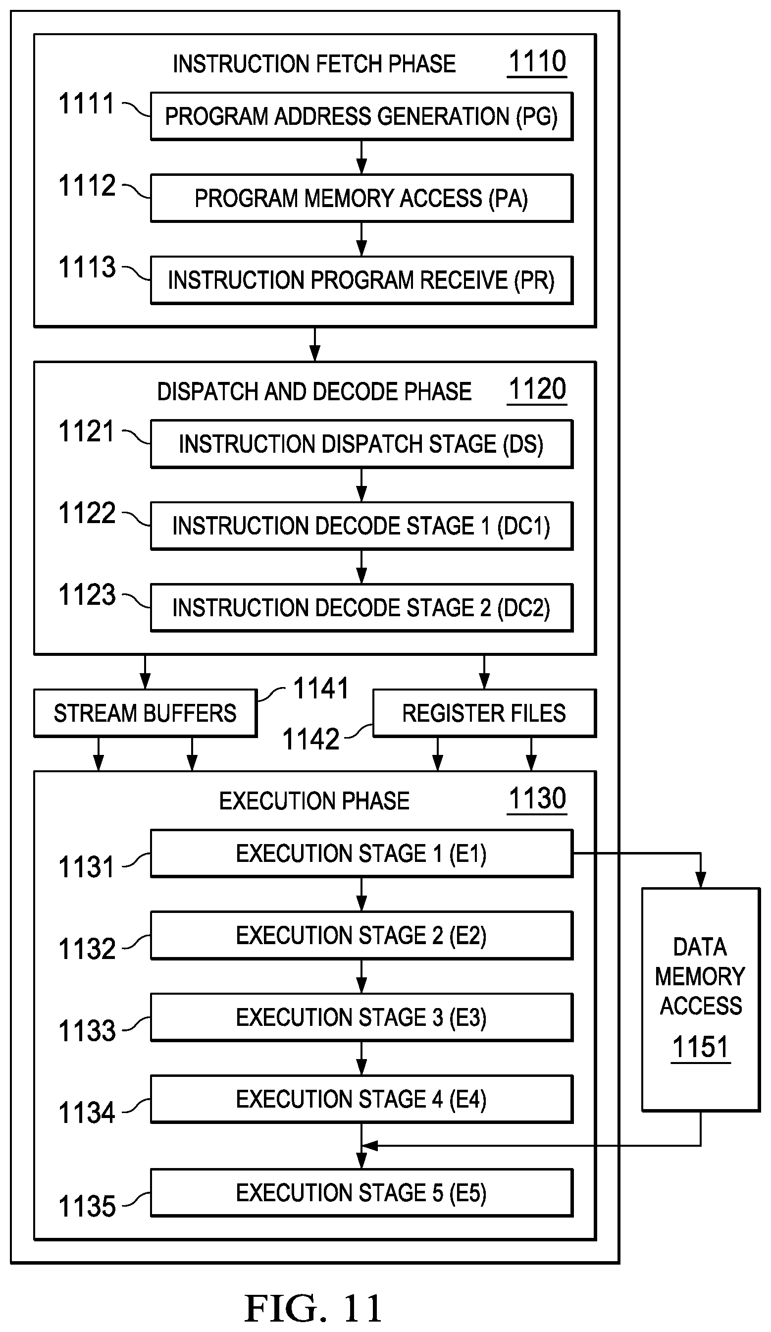
[0011] FIG. 1 illustrates a dual scalar/vector datapath processor according to one embodiment of this invention;
[0012] FIG. 2 illustrates the registers and functional units in the dual scalar/vector datapath processor illustrated in FIG. 1;
[0013] FIG. 3 illustrates a global scalar register file;
[0014] FIG. 4 illustrates a local scalar register file shared by arithmetic functional units;
[0015] FIG. 5 illustrates a local scalar register file shared by multiply functional units;
[0016] FIG. 6 illustrates a local scalar register file shared by the load/store units;
[0017] FIG. 7 illustrates a global vector register file;
[0018] FIG. 8 illustrates a predicate register file;
[0019] FIG. 9 illustrates a local vector register file shared by arithmetic functional units;
[0020] FIG. 10 illustrates a local vector register file shared by a multiply and correlation functional units;
[0021] FIG. 11 illustrates pipeline phases of a central processing unit according to an embodiment of this invention;
[0022] FIG. 12 illustrates sixteen instructions of a single fetch packet;
[0023] FIG. 13 illustrates an example of the instruction coding of instructions used by this invention;
[0024] FIG. 14 illustrates the bit coding of a condition code extension slot 0;
[0025] FIG. 15 illustrates the bit coding of a condition code extension slot 1;
[0026] FIG. 16 illustrates the bit coding of a constant extension slot 0;
[0027] FIG. 17 is a partial block diagram illustrating constant extension; and
[0028] FIG. 18 illustrates the carry control for SIMD operations according to this invention.
DETAILED DESCRIPTION
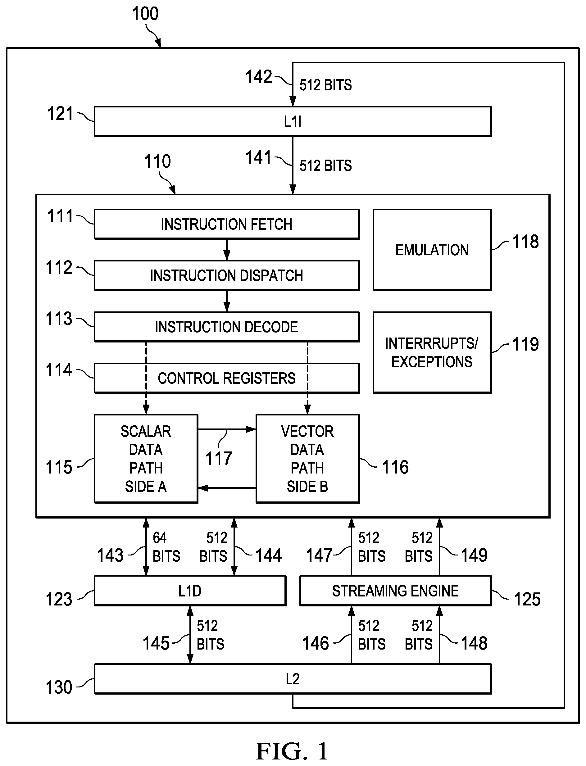
[0029] FIG. 1 illustrates a dual scalar/vector datapath processor according to a preferred embodiment of this invention. Processor 100 includes separate level one instruction cache (L1I) 121 and level one data cache (L1D) 123. Processor 100 includes a level two combined instruction/data cache (L2) 130 that holds both instructions and data. FIG. 1 illustrates connection between level one instruction cache 121 and level two combined instruction/data cache 130 (bus 142). FIG. 1 illustrates connection between level one data cache 123 and level two combined instruction/data cache 130 (bus 145). In the preferred embodiment of processor 100 level two combined instruction/data cache 130 stores both instructions to back up level one instruction cache 121 and data to back up level one data cache 123. In the preferred embodiment level two combined instruction/data cache 130 is further connected to higher level cache and/or main memory in a manner not illustrated in FIG. 1. In the preferred embodiment central processing unit core 110, level one instruction cache 121, level one data cache 123 and level two combined instruction/data cache 130 are formed on a single integrated circuit. This signal integrated circuit optionally includes other circuits.
[0030] Central processing unit core 110 fetches instructions from level one instruction cache 121 as controlled by instruction fetch unit 111. Instruction fetch unit 111 determines the next instructions to be executed and recalls a fetch packet sized set of such instructions. The nature and size of fetch packets are further detailed below. As known in the art, instructions are directly fetched from level one instruction cache 121 upon a cache hit (if these instructions are stored in level one instruction cache 121). Upon a cache miss (the specified instruction fetch packet is not stored in level one instruction cache 121), these instructions are sought in level two combined cache 130. In the preferred embodiment the size of a cache line in level one instruction cache 121 equals the size of a fetch packet. The memory locations of these instructions are either a hit in level two combined cache 130 or a miss. A hit is serviced from level two combined cache 130. A miss is serviced from a higher level of cache (not illustrated) or from main memory (not illustrated). As is known in the art, the requested instruction may be simultaneously supplied to both level one instruction cache 121 and central processing unit core 110 to speed use.
[0031] In the preferred embodiment of this invention, central processing unit core 110 includes plural functional units to perform instruction specified data processing tasks. Instruction dispatch unit 112 determines the target functional unit of each fetched instruction. In the preferred embodiment central processing unit 110 operates as a very long instruction word (VLIW) processor capable of operating on plural instructions in corresponding functional units simultaneously. Preferably a complier organizes instructions in execute packets that are executed together. Instruction dispatch unit 112 directs each instruction to its target functional unit. The functional unit assigned to an instruction is completely specified by the instruction produced by a compiler. The hardware of central processing unit core 110 has no part in this functional unit assignment. In the preferred embodiment instruction dispatch unit 112 may operate on plural instructions in parallel. The number of such parallel instructions is set by the size of the execute packet. This will be further detailed below.
[0032] One part of the dispatch task of instruction dispatch unit 112 is determining whether the instruction is to execute on a functional unit in scalar datapath side A 115 or vector datapath side B 116. An instruction bit within each instruction called the s bit determines which datapath the instruction controls. This will be further detailed below.
[0033] Instruction decode unit 113 decodes each instruction in a current execute packet. Decoding includes identification of the functional unit performing the instruction, identification of registers used to supply data for the corresponding data processing operation from among possible register files and identification of the register destination of the results of the corresponding data processing operation. As further explained below, instructions may include a constant field in place of one register number operand field. The result of this decoding is signals for control of the target functional unit to perform the data processing operation specified by the corresponding instruction on the specified data.
[0034] Central processing unit core 110 includes control registers 114. Control registers 114 store information for control of the functional units in scalar datapath side A 115 and vector datapath side B 116 in a manner not relevant to this invention. This information could be mode information or the like.
[0035] The decoded instructions from instruction decode 113 and information stored in control registers 114 are supplied to scalar datapath side A 115 and vector datapath side B 116. As a result functional units within scalar datapath side A 115 and vector datapath side B 116 perform instruction specified data processing operations upon instruction specified data and store the results in an instruction specified data register or registers. Each of scalar datapath side A 115 and vector datapath side B 116 include plural functional units that preferably operate in parallel. These will be further detailed below in conjunction with FIG. 2. There is a datapath 117 between scalar datapath side A 115 and vector datapath side B 116 permitting data exchange.
[0036] Central processing unit core 110 includes further non-instruction based modules. Emulation unit 118 permits determination of the machine state of central processing unit core 110 in response to instructions. This capability will typically be employed for algorithmic development. Interrupts/exceptions unit 119 enable central processing unit core 110 to be responsive to external, asynchronous events (interrupts) and to respond to attempts to perform improper operations (exceptions).
[0037] Central processing unit core 110 includes streaming engine 125. Streaming engine 125 supplies two data streams from predetermined addresses typically cached in level two combined cache 130 to register files of vector datapath side B. This provides controlled data movement from memory (as cached in level two combined cache 130) directly to register files. This is further detailed below.
[0038] FIG. 1 illustrates exemplary data widths of busses between various parts. Level one instruction cache 121 supplies instructions to instruction fetch unit 111 via bus 141. Bus 141 is preferably a 512-bit bus. Bus 141 is unidirectional from level one instruction cache 121 to central processing unit 110. Level two combined cache 130 supplies instructions to level one instruction cache 121 via bus 142. Bus 142 is preferably a 512-bit bus. Bus 142 is unidirectional from level two combined cache 130 to level one instruction cache 121.
[0039] Level one data cache 123 exchanges data with register files in scalar datapath side A 115 via bus 143. Bus 143 is preferably a 64-bit bus. Level one data cache 123 exchanges data with register files in vector datapath side B 116 via bus 144. Bus 144 is preferably a 512-bit bus. Busses 143 and 144 are illustrated as bidirectional supporting both central processing unit 110 data reads and data writes. Level one data cache 123 exchanges data with level two combined cache 130 via bus 145. Bus 145 is preferably a 512-bit bus. Bus 145 is illustrated as bidirectional supporting cache service for both central processing unit 110 data reads and data writes.
[0040] Level two combined cache 130 supplies data of a first data stream to streaming engine 125 via bus 146. Bus 146 is preferably a 512-bit bus. Streaming engine 125 supplies data of this first data stream to register files of vector datapath side B 116 via bus 147. Bus 147 is preferably a 512-bit bus. Level two combined cache 130 supplies data of a second data stream to streaming engine 125 via bus 148. Bus 148 is preferably a 512-bit bus. Streaming engine 125 supplies data of this second data stream to register files of vector datapath side B 116 via bus 149. Bus 149 is preferably a 512-bit bus. Busses 146, 147, 148 and 149 are illustrated as unidirectional from level two combined cache 130 to streaming engine 125 and to vector datapath side B 116 in accordance with the preferred embodiment of this invention.
[0041] In the preferred embodiment of this invention, both level one data cache 123 and level two combined cache 130 may be configured as selected amounts of cache or directly addressable memory in accordance with U.S. Pat. No. 6,606,686 entitled UNIFIED MEMORY SYSTEM ARCHITECTURE INCLUDING CACHE AND DIRECTLY ADDRESSABLE STATIC RANDOM ACCESS MEMORY.
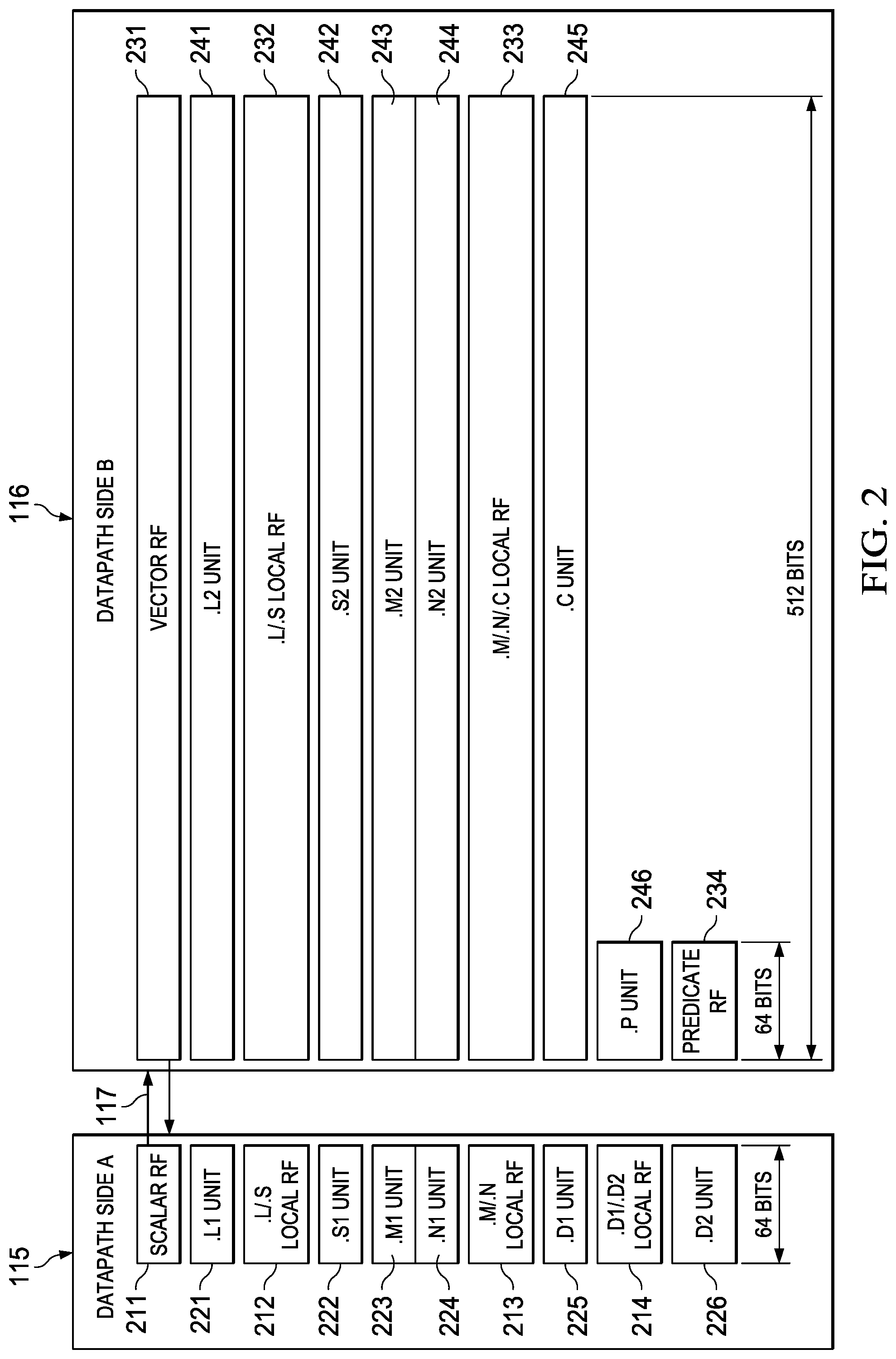
[0042] FIG. 2 illustrates further details of functional units and register files within scalar datapath side A 115 and vector datapath side B 116. Scalar datapath side A 115 includes global scalar register file 211, L1/S1 local register file 212, M1/N1 local register file 213 and D1/D2 local register file 214. Scalar datapath side A 115 includes L1 unit 221, S1 unit 222, M1 unit 223, N1 unit 224, D1 unit 225 and D2 unit 226. Vector datapath side B 116 includes global scalar register file 231, L2/S2 local register file 232, M2/N2/C local register file 233 and predicate register file 234. Vector datapath side B 116 includes L2 unit 241, S2 unit 242, M2 unit 243, N2 unit 244, C unit 245 and P unit 246. There are limitations upon which functional units may read from or write to which register files. These will be detailed below.
[0043] Scalar datapath side A 115 includes L1 unit 221. L1 unit 221 generally accepts two 64-bit operands and produces one 64-bit result. The two operands are each recalled from an instruction specified register in either global scalar register file 211 or L1/S1 local register file 212. L1 unit 221 preferably performs the following instruction selected operations: 64-bit add/subtract operations; 32-bit min/max operations; 8-bit Single Instruction Multiple Data (SIMD) instructions such as sum of absolute value, minimum and maximum determinations; circular min/max operations; and various move operations between register files. The result may be written into an instruction specified register of global scalar register file 211, L1/S1 local register file 212, M1/N1 local register file 213 or D1/D2 local register file 214.
[0044] Scalar datapath side A 115 includes S1 unit 222. S1 unit 222 generally accepts two 64-bit operands and produces one 64-bit result. The two operands are each recalled from an instruction specified register in either global scalar register file 211 or L1/S1 local register file 212. S1 unit 222 preferably performs the same type operations as L1 unit 221. There optionally may be slight variations between the data processing operations supported by L1 unit 221 and S1 unit 222. The result may be written into an instruction specified register of global scalar register file 211, L1/S1 local register file 212, M1/N1 local register file 213 or D1/D2 local register file 214.
[0045] Scalar datapath side A 115 includes M1 unit 223. M1 unit 223 generally accepts two 64-bit operands and produces one 64-bit result. The two operands are each recalled from an instruction specified register in either global scalar register file 211 or M1/N1 local register file 213. M1 unit 223 preferably performs the following instruction selected operations: 8-bit multiply operations; complex dot product operations; 32-bit bit count operations; complex conjugate multiply operations; and bit-wise Logical Operations, moves, adds and subtracts. The result may be written into an instruction specified register of global scalar register file 211, L1/S1 local register file 212, M1/N1 local register file 213 or D1/D2 local register file 214.
[0046] Scalar datapath side A 115 includes N1 unit 224. N1 unit 224 generally accepts two 64-bit operands and produces one 64-bit result. The two operands are each recalled from an instruction specified register in either global scalar register file 211 or M1/N1 local register file 213. N1 unit 224 preferably performs the same type operations as M1 unit 223. There may be certain double operations (called dual issued instructions) that employ both the M1 unit 223 and the N1 unit 224 together. The result may be written into an instruction specified register of global scalar register file 211, L1/S1 local register file 212, M1/N1 local register file 213 or D1/D2 local register file 214.
[0047] Scalar datapath side A 115 includes D1 unit 225 and D2 unit 226. D1 unit 225 and D2 unit 226 generally each accept two 64-bit operands and each produce one 64-bit result. D1 unit 225 and D2 unit 226 generally perform address calculations and corresponding load and store operations. D1 unit 225 is used for scalar loads and stores of 64 bits. D2 unit 226 is used for vector loads and stores of 512 bits. D1 unit 225 and D2 unit 226 preferably also perform: swapping, pack and unpack on the load and store data; 64-bit SIMD arithmetic operations; and 64-bit bit-wise logical operations. D1/D2 local register file 214 will generally store base and offset addresses used in address calculations for the corresponding loads and stores. The two operands are each recalled from an instruction specified register in either global scalar register file 211 or D1/D2 local register file 214. The calculated result may be written into an instruction specified register of global scalar register file 211, L1/S1 local register file 212, M1/N1 local register file 213 or D1/D2 local register file 214.
[0048] Vector datapath side B 116 includes L2 unit 241. L2 unit 241 generally accepts two 512-bit operands and produces one 512-bit result. The two operands are each recalled from an instruction specified register in either global vector register file 231, L2/S2 local register file 232 or predicate register file 234. L2 unit 241 preferably performs instruction similar to L1 unit 221 except on wider 512-bit data. The result may be written into an instruction specified register of global vector register file 231, L2/S2 local register file 222, M2/N2/C local register file 233 or predicate register file 234.
[0049] Vector datapath side B 116 includes S2 unit 242. S2 unit 242 generally accepts two 512-bit operands and produces one 512-bit result. The two operands are each recalled from an instruction specified register in either global vector register file 231, L2/S2 local register file 232 or predicate register file 234. S2 unit 242 preferably performs instructions similar to S1 unit 222 except on wider 512-bit data. The result may be written into an instruction specified register of global vector register file 231, L2/S2 local register file 232, M2/N2/C local register file 233 or predicate register file 234.
[0050] Vector datapath side B 116 includes M2 unit 243. M2 unit 243 generally accepts two 512-bit operands and produces one 512-bit result. The two operands are each recalled from an instruction specified register in either global vector register file 231 or M2/N2/C local register file 233. M2 unit 243 preferably performs instructions similar to M1 unit 223 except on wider 512-bit data. The result may be written into an instruction specified register of global vector register file 231, L2/S2 local register file 232 or M2/N2/C local register file 233.
[0051] Vector datapath side B 116 includes N2 unit 244. N2 unit 244 generally accepts two 512-bit operands and produces one 512-bit result. The two operands are each recalled from an instruction specified register in either global vector register file 231 or M2/N2/C local register file 233. N2 unit 244 preferably performs the same type operations as M2 unit 243. There may be certain double operations (called dual issued instructions) that employ both M2 unit 243 and the N2 unit 244 together. The result may be written into an instruction specified register of global vector register file 231, L2/S2 local register file 232 or M2/N2/C local register file 233.
[0052] Vector datapath side B 116 includes C unit 245. C unit 245 generally accepts two 512-bit operands and produces one 512-bit result. The two operands are each recalled from an instruction specified register in either global vector register file 231 or M2/N2/C local register file 233. C unit 245 preferably performs: "Rake" and "Search" instructions; up to 512 2-bit PN*8-bit multiplies I/Q complex multiplies per clock cycle; 8-bit and 16-bit Sum-of-Absolute-Difference (SAD) calculations, up to 512 SADs per clock cycle; horizontal add and horizontal min/max instructions; and vector permutes instructions. C unit 245 includes also contains 4 vector control registers (CUCR0 to CUCR3) used to control certain operations of C unit 245 instructions. Control registers CUCR0 to CUCR3 are used as operands in certain C unit 245 operations. Control registers CUCR0 to CUCR3 are preferably used: in control of a general permutation instruction (VPERM); and as masks for SIMD multiple DOT product operations (DOTPM) and SIMD multiple Sum-of-Absolute-Difference (SAD) operations. Control register CUCR0 is preferably used to store the polynomials for Galois Field Multiply operations (GFMPY). Control register CUCR1 is preferably used to store the Galois field polynomial generator function.
[0053] Vector datapath side B 116 includes P unit 246. P unit 246 performs basic logic operations on registers of local predicate register file 234. P unit 246 has direct access to read from and write to predication register file 234. These operations include AND, ANDN, OR, XOR, NOR, BITR, NEG, SET, BITCNT, RMBD, BIT Decimate and Expand. A commonly expected use of P unit 246 includes manipulation of the SIMD vector comparison results for use in control of a further SIMD vector operation.
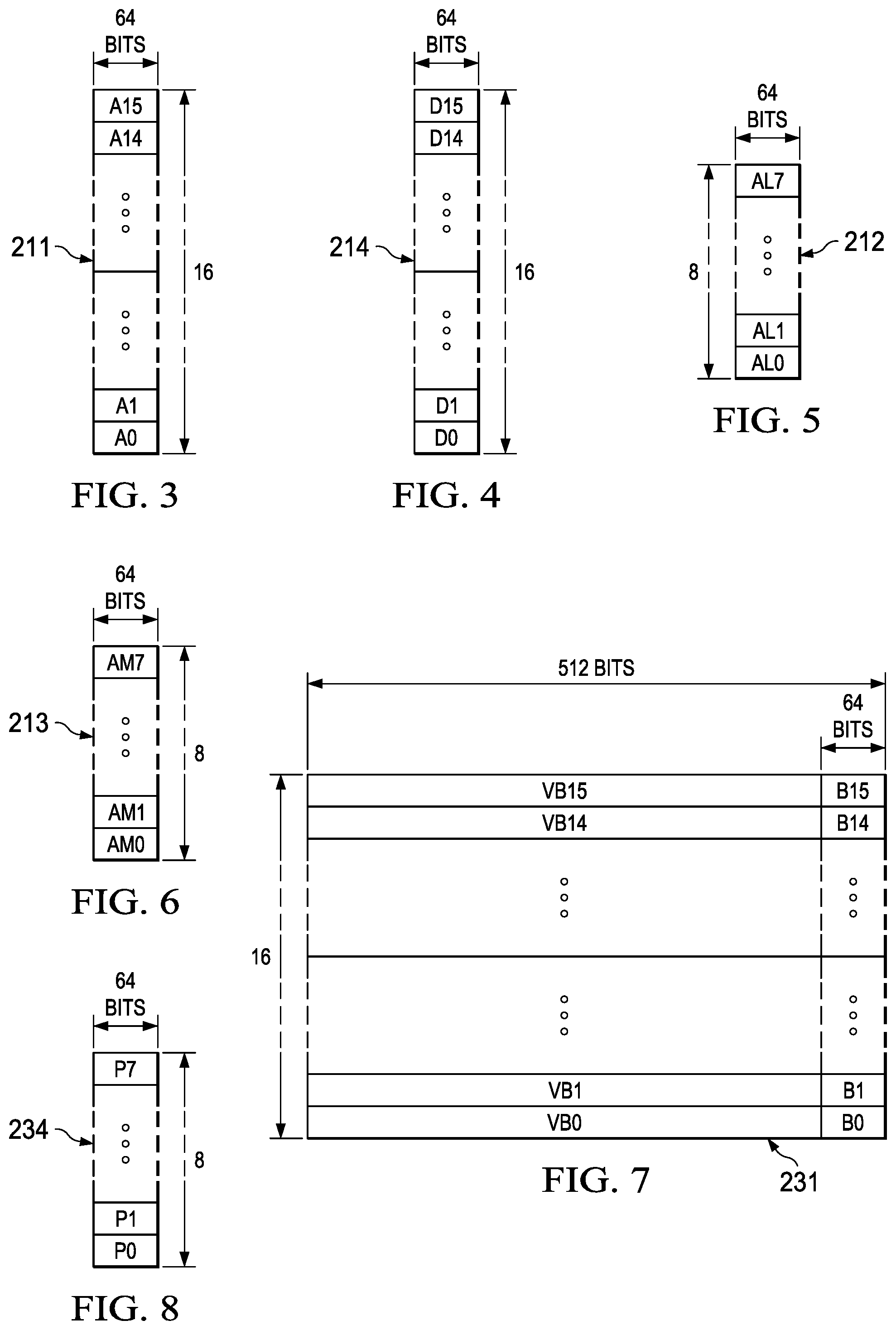
[0054] FIG. 3 illustrates global scalar register file 211. There are 16 independent 64-bit wide scalar registers designated A0 to A15. Each register of global scalar register file 211 can be read from or written to as 64-bits of scalar data. All scalar datapath side A 115 functional units (L1 unit 221, S1 unit 222, M1 unit 223, N1 unit 224, D1 unit 225 and D2 unit 226) can read or write to global scalar register file 211. Global scalar register file 211 may be read as 32-bits or as 64-bits and may only be written to as 64-bits. The instruction executing determines the read data size. Vector datapath side B 116 functional units (L2 unit 241, S2 unit 242, M2 unit 243, N2 unit 244, C unit 245 and P unit 246) can read from global scalar register file 211 via crosspath 117 under restrictions that will be detailed below.
[0055] FIG. 4 illustrates D1/D2 local register file 214. There are 16 independent 64-bit wide scalar registers designated D0 to D16. Each register of D1/D2 local register file 214 can be read from or written to as 64-bits of scalar data. All scalar datapath side A 115 functional units (L1 unit 221, S1 unit 222, M1 unit 223, N1 unit 224, D1 unit 225 and D2 unit 226) can write to global scalar register file 211. Only D1 unit 225 and D2 unit 226 can read from D1/D2 local scalar register file 214. It is expected that data stored in D1/D2 local scalar register file 214 will include base addresses and offset addresses used in address calculation.
[0056] FIG. 5 illustrates L1/S1 local register file 212. The embodiment illustrated in FIG. 5 has 8 independent 64-bit wide scalar registers designated AL0 to AL7. The preferred instruction coding (see FIG. 13) permits L1/S1 local register file 212 to include up to 16 registers. The embodiment of FIG. 5 implements only 8 registers to reduce circuit size and complexity. Each register of L1/S1 local register file 212 can be read from or written to as 64-bits of scalar data. All scalar datapath side A 115 functional units (L1 unit 221, S1 unit 222, M1 unit 223, N1 unit 224, D1 unit 225 and D2 unit 226) can write to L1/S1 local scalar register file 212. Only L1 unit 221 and S1 unit 222 can read from L1/S1 local scalar register file 212.
[0057] FIG. 6 illustrates M1/N1 local register file 213. The embodiment illustrated in FIG. 6 has 8 independent 64-bit wide scalar registers designated AM0 to AM7. The preferred instruction coding (see FIG. 13) permits M1/N1 local register file 213 to include up to 16 registers. The embodiment of FIG. 6 implements only 8 registers to reduce circuit size and complexity. Each register of M1/N1 local register file 213 can be read from or written to as 64-bits of scalar data. All scalar datapath side A 115 functional units (L1 unit 221, S1 unit 222, M1 unit 223, N1 unit 224, D1 unit 225 and D2 unit 226) can write to M1/N1 local scalar register file 213. Only M1 unit 223 and N1 unit 224 can read from M1/N1 local scalar register file 213.
[0058] FIG. 7 illustrates global vector register file 231. There are 16 independent 512-bit wide scalar registers. Each register of global vector register file 231 can be read from or written to as 64-bits of scalar data designated B0 to B15. Each register of global vector register file 231 can be read from or written to as 512-bits of vector data designated VB0 to VB15. The instruction type determines the data size. All vector datapath side B 116 functional units (L2 unit 241, S2 unit 242, M2 unit 243, N2 unit 244, C unit 245 and P unit 246) can read or write to global vector register file 231. Scalar datapath side A 115 functional units (L1 unit 221, S1 unit 222, M1 unit 223, N1 unit 224, D1 unit 225 and D2 unit 226) can read from global vector register file 231 via crosspath 117 under restrictions that will be detailed below.
[0059] FIG. 8 illustrates P local register file 234. There are 8 independent 64-bit wide registers designated P0 to P15. Each register of P local register file 234 can be read from or written to as 64-bits of scalar data. Vector datapath side B 116 functional units L2 unit 241, S2 unit 242, C unit 244 and P unit 246 can write to P local register file 234. Only L2 unit 241, S2 unit 242 and P unit 246 can read from P local scalar register file 234. A commonly expected use of P local register file 234 includes: writing one bit SIMD vector comparison results from L2 unit 241, S2 unit 242 or C unit 245; manipulation of the SIMD vector comparison results by P unit 246; and use of the manipulated results in control of a further SIMD vector operation.
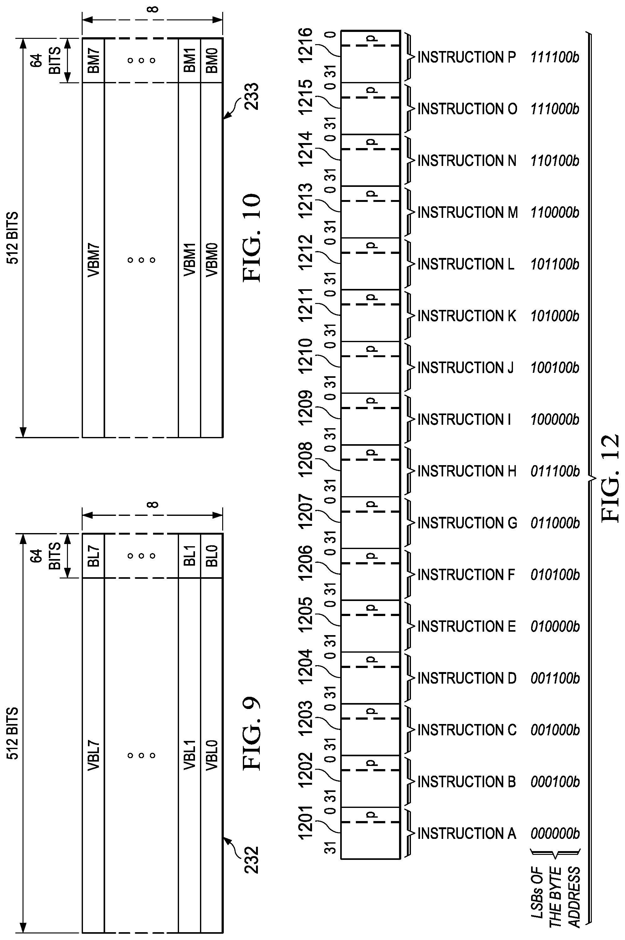
[0060] FIG. 9 illustrates L2/S2 local register file 232. The embodiment illustrated in FIG. 9 has 8 independent 512-bit wide scalar registers. The preferred instruction coding (see FIG. 13) permits L2/S2 local register file 232 to include up to 16 registers. The embodiment of FIG. 9 implements only 8 registers to reduce circuit size and complexity. Each register of L2/S2 local vector register file 232 can be read from or written to as 64-bits of scalar data designated BL0 to BL7. Each register of L2/S2 local vector register file 232 can be read from or written to as 512-bits of vector data designated VBL0 to VBL7. The instruction type determines the data size. All vector datapath side B 116 functional units (L2 unit 241, S2 unit 242, M2 unit 243, N2 unit 24, C unit 245 and P unit 246) can write to L2/S2 local vector register file 232. Only L2 unit 241 and S2 unit 242 can read from L2/S2 local vector register file 232.
[0061] FIG. 10 illustrates M2/N2/C local register file 233. The embodiment illustrated in FIG. 10 has 8 independent 512-bit wide scalar registers. The preferred instruction coding (see FIG. 13) permits M2/N2/C local register file 233 to include up to 16 registers. The embodiment of FIG. 10 implements only 8 registers to reduce circuit size and complexity. Each register of M2/N2/C local vector register file 233 can be read from or written to as 64-bits of scalar data designated BM0 to BM7. Each register of M2/N2/C local vector register file 233 can be read from or written to as 512-bits of vector data designated VBM0 to VBM7. All vector datapath side B 116 functional units (L2 unit 241, S2 unit 242, M2 unit 243, N2 unit 244, C unit 245 and P unit 246) can write to M2/N2/C local vector register file 233. Only M2 unit 243, N2 unit 244 and C unit 245 can read from M2/N2/C local vector register file 233.
[0062] Crosspath 117 permits limited exchange of data between scalar datapath side A 115 and vector datapath side B 116. During each operational cycle one 64-bit data word can be recalled from global scalar register file A 211 for use as an operand by one or more functional units of vector datapath side B 116 and one 64-bit data word can be recalled from global vector register file 231 for use as an operand by one or more functional units of scalar datapath side A 115. Any scalar datapath side A 115 functional unit (L1 unit 221, S1 unit 222, M1 unit 223, N1 unit 224, D1 unit 225 and D2 unit 226) may read a 64-bit operand from global vector register file 231. This 64-bit operand is the least significant bits of the 512-bit data in the accessed register of global vector register file 231. Plural scalar datapath side A 115 functional units may employ the same 64-bit crosspath data as an operand during the same operational cycle. However, only one 64-bit operand is transferred from vector datapath side B 116 to scalar datapath side A 115 in any single operational cycle. Any vector datapath side B 116 functional unit (L2 unit 241, S2 unit 242, M2 unit 243, N2 unit 244, C unit 245 and P unit 246) may read a 64-bit operand from global scalar register file 211. If the corresponding instruction is a scalar instruction, the crosspath operand data is treated as any other 64-bit operand. If the corresponding instruction is a vector instruction, the upper 448 bits of the operand are zero filled. Plural vector datapath side B 116 functional units may employ the same 64-bit crosspath data as an operand during the same operational cycle. Only one 64-bit operand is transferred from scalar datapath side A 115 to vector datapath side B 116 in any single operational cycle.
[0063] Streaming engine 125 transfers data in certain restricted circumstances. Streaming engine 125 controls two data streams. A stream consists of a sequence of elements of a particular type. Programs that operate on streams read the data sequentially, operating on each element in turn. Every stream has the following basic properties. The stream data have a well-defined beginning and ending in time. The stream data have fixed element size and type throughout the stream. The stream data have fixed sequence of elements. Thus programs cannot seek randomly within the stream. The stream data is read-only while active. Programs cannot write to a stream while simultaneously reading from it. Once a stream is opened streaming engine 125: calculates the address; fetches the defined data type from level two unified cache (which may require cache service from a higher level memory); performs data type manipulation such as zero extension, sign extension, data element sorting/swapping such as matrix transposition; and delivers the data directly to the programmed data register file within CPU 110. Streaming engine 125 is thus useful for real-time digital filtering operations on well-behaved data. Streaming engine 125 frees these memory fetch tasks from the corresponding CPU enabling other processing functions.
[0064] Streaming engine 125 provides the following benefits. Streaming engine 125 permits multi-dimensional memory accesses. Streaming engine 125 increases the available bandwidth to the functional units. Streaming engine 125 minimizes the number of cache miss stalls since the stream buffer bypasses level one data cache 123. Streaming engine 125 reduces the number of scalar operations required to maintain a loop. Streaming engine 125 manages address pointers. Streaming engine 125 handles address generation automatically freeing up the address generation instruction slots and D1 unit 225 and D2 unit 226 for other computations.
[0065] CPU 110 operates on an instruction pipeline. Instructions are fetched in instruction packets of fixed length further described below. All instructions require the same number of pipeline phases for fetch and decode, but require a varying number of execute phases.
[0066] FIG. 11 illustrates the following pipeline phases: program fetch phase 1110, dispatch and decode phases 1120 and execution phases 1130. Program fetch phase 1110 includes three stages for all instructions. Dispatch and decode phases 1120 include three stages for all instructions. Execution phase 1130 includes one to four stages dependent on the instruction.
[0067] Fetch phase 1110 includes program address generation stage 1111 (PG), program access stage 1112 (PA) and program receive stage 1113 (PR). During program address generation stage 1111 (PG), the program address is generated in the CPU and the read request is sent to the memory controller for the level one instruction cache L1I. During the program access stage 1112 (PA) the level one instruction cache L1I processes the request, accesses the data in its memory and sends a fetch packet to the CPU boundary. During the program receive stage 1113 (PR) the CPU registers the fetch packet.
[0068] Instructions are always fetched sixteen 32-bit wide slots, constituting a fetch packet, at a time. FIG. 12 illustrates 16 instructions 1201 to 1216 of a single fetch packet. Fetch packets are aligned on 512-bit (16-word) boundaries. The preferred embodiment employs a fixed 32-bit instruction length. Fixed length instructions are advantageous for several reasons. Fixed length instructions enable easy decoder alignment. A properly aligned instruction fetch can load plural instructions into parallel instruction decoders. Such a properly aligned instruction fetch can be achieved by predetermined instruction alignment when stored in memory (fetch packets aligned on 512-bit boundaries) coupled with a fixed instruction packet fetch. An aligned instruction fetch permits operation of parallel decoders on instruction-sized fetched bits. Variable length instructions require an initial step of locating each instruction boundary before they can be decoded. A fixed length instruction set generally permits more regular layout of instruction fields. This simplifies the construction of each decoder which is an advantage for a wide issue VLIW central processor.
[0069] The execution of the individual instructions is partially controlled by a p bit in each instruction. This p bit is preferably bit 0 of the 32-bit wide slot. The p bit determines whether an instruction executes in parallel with a next instruction. Instructions are scanned from lower to higher address. If the p bit of an instruction is 1, then the next following instruction (higher memory address) is executed in parallel with (in the same cycle as) that instruction. If the p bit of an instruction is 0, then the next following instruction is executed in the cycle after the instruction.
[0070] CPU 110 and level one instruction cache L1I 121 pipelines are de-coupled from each other. Fetch packet returns from level one instruction cache L1I can take different number of clock cycles, depending on external circumstances such as whether there is a hit in level one instruction cache 121 or a hit in level two combined cache 130. Therefore program access stage 1112 (PA) can take several clock cycles instead of 1 clock cycle as in the other stages.
[0071] The instructions executing in parallel constitute an execute packet. In the preferred embodiment an execute packet can contain up to sixteen instructions. No two instructions in an execute packet may use the same functional unit. A slot is one of five types: 1) a self-contained instruction executed on one of the functional units of CPU 110 (L1 unit 221, S1 unit 222, M1 unit 223, N1 unit 224, D1 unit 225, D2 unit 226, L2 unit 241, S2 unit 242, M2 unit 243, N2 unit 244, C unit 245 and P unit 246); 2) a unitless instruction such as a NOP (no operation) instruction or multiple NOP instruction; 3) a branch instruction; 4) a constant field extension; and 5) a conditional code extension. Some of these slot types will be further explained below.
[0072] Dispatch and decode phases 1120 include instruction dispatch to appropriate execution unit stage 1121 (DS), instruction pre-decode stage 1122 (DC1), and instruction decode, operand reads stage 1123 (DC2). During instruction dispatch to appropriate execution unit stage 1121 (DS), the fetch packets are split into execute packets and assigned to the appropriate functional units. During instruction pre-decode stage 1122 (DC1), the source registers, destination registers and associated paths are decoded for the execution of the instructions in the functional units. During the instruction decode, operand reads stage 1123 (DC2), more detailed unit decodes are done, as well as reading operands from the register files.
[0073] Execution phases 1130 includes execution stages 1131 to 1135 (E1 to E5). Different types of instructions require different numbers of these stages to complete their execution. These stages of the pipeline play an important role in understanding the device state at CPU cycle boundaries.
[0074] During execute 1 stage 1131 (E1) the conditions for the instructions are evaluated and operands are operated on. As illustrated in FIG. 11, execute 1 stage 1131 may receive operands from a stream buffer 1141 and one of the register files shown schematically as 1142. For load and store instructions, address generation is performed and address modifications are written to a register file. For branch instructions, branch fetch packet in PG phase 1111 is affected. As illustrated in FIG. 11, load and store instructions access memory here shown schematically as memory 1151. For single-cycle instructions, results are written to a destination register file. This assumes that any conditions for the instructions are evaluated as true. If a condition is evaluated as false, the instruction does not write any results or have any pipeline operation after execute 1 stage 1131.
[0075] During execute 2 stage 1132 (E2) load instructions send the address to memory. Store instructions send the address and data to memory. Single-cycle instructions that saturate results set the SAT bit in the control status register (CSR) if saturation occurs. For 2-cycle instructions, results are written to a destination register file.
[0076] During execute 3 stage 1133 (E3) data memory accesses are performed. Any multiply instructions that saturate results set the SAT bit in the control status register (CSR) if saturation occurs. For 3-cycle instructions, results are written to a destination register file.
[0077] During execute 4 stage 1134 (E4) load instructions bring data to the CPU boundary. For 4-cycle instructions, results are written to a destination register file.
[0078] During execute 5 stage 1135 (E5) load instructions write data into a register. This is illustrated schematically in FIG. 11 with input from memory 1151 to execute 5 stage 1135.
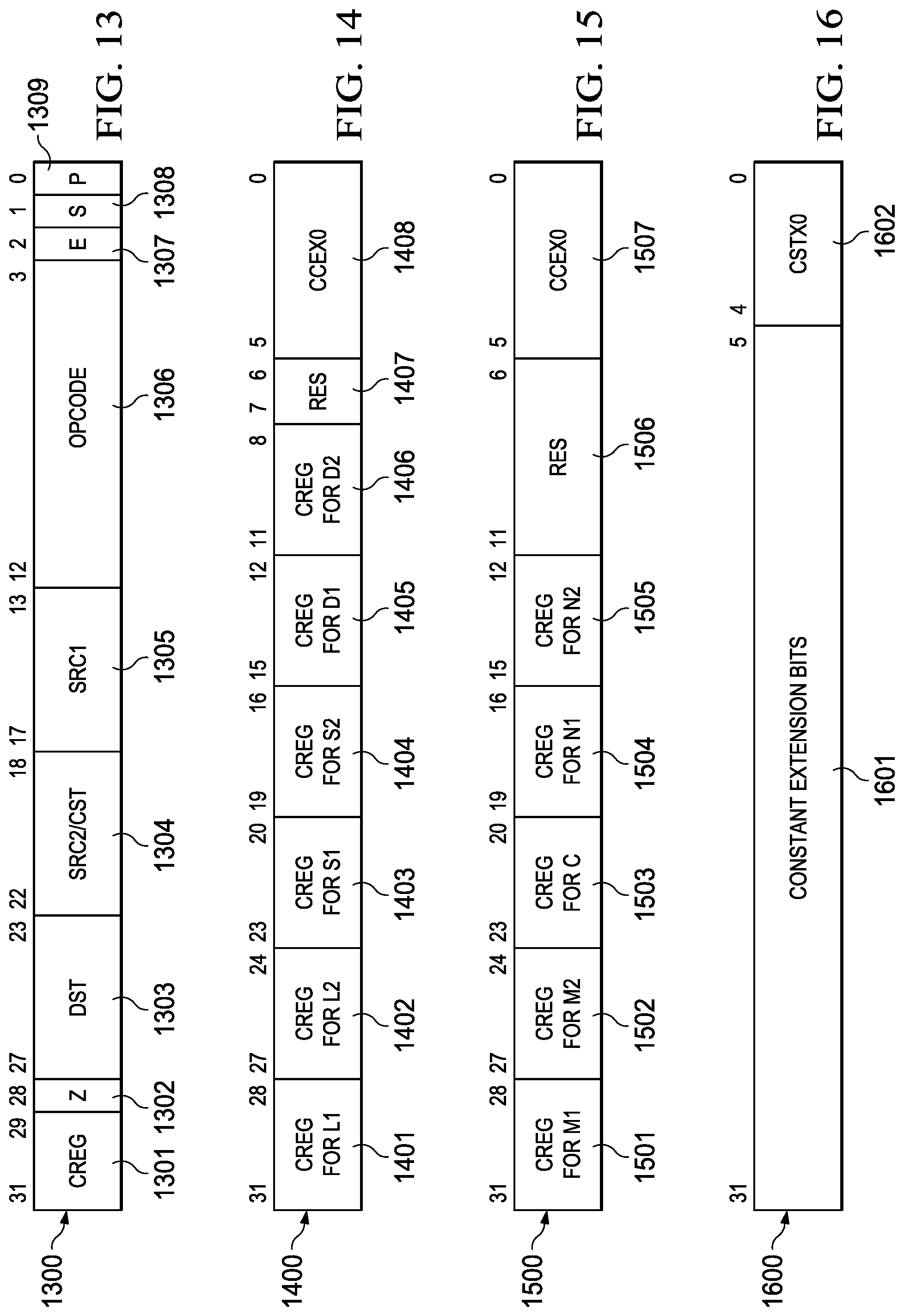
[0079] FIG. 13 illustrates an example of the instruction coding 1300 of functional unit instructions used by this invention. Those skilled in the art would realize that other instruction codings are feasible and within the scope of this invention. Each instruction consists of 32 bits and controls the operation of one of the individually controllable functional units (L1 unit 221, S1 unit 222, M1 unit 223, N1 unit 224, D1 unit 225, D2 unit 226, L2 unit 241, S2 unit 242, M2 unit 243, N2 unit 244, C unit 245 and P unit 246). The bit fields are defined as follows.
[0080] The creg field 1301 (bits 29 to 31) and the z bit 1302 (bit 28) are optional fields used in conditional instructions. These bits are used for conditional instructions to identify the predicate register and the condition. The z bit 1302 (bit 28) indicates whether the predication is based upon zero or not zero in the predicate register. If z=1, the test is for equality with zero. If z=0, the test is for nonzero. The case of creg=0 and z=0 is treated as always true to allow unconditional instruction execution. The creg field 1301 and the z field 1302 are encoded in the instruction as shown in Table 1.
TABLE-US-00001 TABLE 1 Conditional creg z Register 31 30 29 28 Unconditional 0 0 0 0 Reserved 0 0 0 1 A0 0 0 1 z A1 0 1 0 z A2 0 1 1 z A3 1 0 0 z A4 1 0 1 z A5 1 1 0 z Reserved 1 1 x x
Execution of a conditional instruction is conditional upon the value stored in the specified data register. This data register is in the global scalar register file 211 for all functional units. Note that "z" in the z bit column refers to the zero/not zero comparison selection noted above and "x" is a don't care state. This coding can only specify a subset of the 16 global registers as predicate registers. This selection was made to preserve bits in the instruction coding. Note that unconditional instructions do not have these optional bits. For unconditional instructions these bits in fields 1301 and 1302 (28 to 31) are preferably used as additional opcode bits.
[0081] The dst field 1303 (bits 23 to 27) specifies a register in a corresponding register file as the destination of the instruction results.
[0082] The src2/cst field 1304 (bits 18 to 22) has several meanings depending on the instruction opcode field (bits 3 to 12 for all instructions and additionally bits 28 to 31 for unconditional instructions). The first meaning specifies a register of a corresponding register file as the second operand. The second meaning is an immediate constant. Depending on the instruction type, this is treated as an unsigned integer and zero extended to a specified data length or is treated as a signed integer and sign extended to the specified data length.
[0083] The src1 field 1305 (bits 13 to 17) specifies a register in a corresponding register file as the first source operand.
[0084] The opcode field 1306 (bits 3 to 12) for all instructions (and additionally bits 28 to 31 for unconditional instructions) specifies the type of instruction and designates appropriate instruction options. This includes unambiguous designation of the functional unit used and operation performed. A detailed explanation of the opcode is beyond the scope of this invention except for the instruction options detailed below.
[0085] The e bit 1307 (bit 2) is only used for immediate constant instructions where the constant may be extended. If e=1, then the immediate constant is extended in a manner detailed below. If e=0, then the immediate constant is not extended. In that case the immediate constant is specified by the src2/cst field 1304 (bits 18 to 22). Note that this e bit 1307 is used for only some instructions. Accordingly, with proper coding this e bit 1307 may be omitted from instructions which do not need it and this bit used as an additional opcode bit.
[0086] The s bit 1308 (bit 1) designates scalar datapath side A 115 or vector datapath side B 116. If s=0, then scalar datapath side A 115 is selected. This limits the functional unit to L1 unit 221, S1 unit 222, M1 unit 223, N1 unit 224, D1 unit 225 and D2 unit 226 and the corresponding register files illustrated in FIG. 2. Similarly, s=1 selects vector datapath side B 116 limiting the functional unit to L2 unit 241, S2 unit 242, M2 unit 243, N2 unit 244, P unit 246 and the corresponding register file illustrated in FIG. 2.
[0087] The p bit 1309 (bit 0) marks the execute packets. The p-bit determines whether the instruction executes in parallel with the following instruction. The p-bits are scanned from lower to higher address. If p=1 for the current instruction, then the next instruction executes in parallel with the current instruction. If p=0 for the current instruction, then the next instruction executes in the cycle after the current instruction. All instructions executing in parallel constitute an execute packet. An execute packet can contain up to twelve instructions. Each instruction in an execute packet must use a different functional unit.
[0088] There are two different condition code extension slots. Each execute packet can contain one each of these unique 32-bit condition code extension slots which contains the 4-bit creg/z fields for the instructions in the same execute packet. FIG. 14 illustrates the coding for condition code extension slot 0 and FIG. 15 illustrates the coding for condition code extension slot 1.
[0089] FIG. 14 illustrates the coding for condition code extension slot 0 1400 having 32 bits. Field 1401 (bits 28 to 31) specify 4 creg/z bits assigned to the L1 unit 221 instruction in the same execute packet. Field 1402 (bits 27 to 24) specify 4 creg/z bits assigned to the L2 unit 241 instruction in the same execute packet. Field 1403 (bits 20 to 23) specify 4 creg/z bits assigned to the S1 unit 222 instruction in the same execute packet. Field 1404 (bits 16 to 19) specify 4 creg/z bits assigned to the S2 unit 242 instruction in the same execute packet. Field 1405 (bits 12 to 15) specify 4 creg/z bits assigned to the D1 unit 225 instruction in the same execute packet. Field 1406 (bits 8 to 11) specify 4 creg/z bits assigned to the D2 unit 226 instruction in the same execute packet. Field 1407 (bits 6 and 7) is unused/reserved. Field 1408 (bits 0 to 5) are coded a set of unique bits (CCEX0) to identify the condition code extension slot 0. Once this unique ID of condition code extension slot 0 is detected, the corresponding creg/z bits are employed to control conditional execution of any L1 unit 221, L2 unit 241, S1 unit 222, S2 unit 242, D1 unit 225 and D2 unit 226 instruction in the same execution packet. These creg/z bits are interpreted as shown in Table 1. If the corresponding instruction is conditional (includes creg/z bits) the corresponding bits in the condition code extension slot 0 override the condition code bits in the instruction. Note that no execution packet can have more than one instruction directed to a particular execution unit. No execute packet of instructions can contain more than one condition code extension slot 0. Thus the mapping of creg/z bits to functional unit instruction is unambiguous. Setting the creg/z bits equal to "0000" makes the instruction unconditional. Thus a properly coded condition code extension slot 0 can make some corresponding instructions conditional and some unconditional.
[0090] FIG. 15 illustrates the coding for condition code extension slot 1 1500 having 32 bits. Field 1501 (bits 28 to 31) specify 4 creg/z bits assigned to the M1 unit 223 instruction in the same execute packet. Field 1502 (bits 27 to 24) specify 4 creg/z bits assigned to the M2 unit 243 instruction in the same execute packet. Field 1503 (bits 19 to 23) specify 4 creg/z bits assigned to the C unit 245 instruction in the same execute packet. Field 1504 (bits 16 to 19) specify 4 creg/z bits assigned to the N1 unit 224 instruction in the same execute packet. Field 1505 (bits 12 to 15) specify 4 creg/z bits assigned to the N2 unit 244 instruction in the same execute packet. Field 1506 (bits 6 to 11) is unused/reserved. Field 1507 (bits 0 to 5) are coded a set of unique bits (CCEX1) to identify the condition code extension slot 1. Once this unique ID of condition code extension slot 1 is detected, the corresponding creg/z bits are employed to control conditional execution of any M1 unit 223, M2 unit 243, C unit 245, N1 unit 224 and N2 unit 244 instruction in the same execution packet. These creg/z bits are interpreted as shown in Table 1. If the corresponding instruction is conditional (includes creg/z bits) the corresponding bits in the condition code extension slot 1 override the condition code bits in the instruction. Note that no execution packet can have more than one instruction directed to a particular execution unit. No execute packet of instructions can contain more than one condition code extension slot 1. Thus the mapping of creg/z bits to functional unit instruction is unambiguous. Setting the creg/z bits equal to "0000" makes the instruction unconditional. Thus a properly coded condition code extension slot 1 can make some instructions conditional and some unconditional.
[0091] It is feasible for both condition code extension slot 0 and condition code extension slot 1 to include a p bit to define an execute packet as described above in conjunction with FIG. 13. In the preferred embodiment, as illustrated in FIGS. 14 and 15, code extension slot 0 and condition code extension slot 1 preferably have bit 0 (p bit) always encoded as 1. Thus neither condition code extension slot 0 not condition code extension slot 1 can be in the last instruction slot of an execute packet.
[0092] There are two different constant extension slots. Each execute packet can contain one each of these unique 32-bit constant extension slots which contains 27 bits to be concatenated as high order bits with the 5-bit constant field 1305 to form a 32-bit constant. As noted in the instruction coding description above only some instructions define the src2/cst field 1304 as a constant rather than a source register identifier. At least some of those instructions may employ a constant extension slot to extend this constant to 32 bits.
[0093] FIG. 16 illustrates the fields of constant extension slot 0 1600. Each execute packet may include one instance of constant extension slot 0 and one instance of constant extension slot 1. FIG. 16 illustrates that constant extension slot 0 1600 includes two fields. Field 1601 (bits 5 to 31) constitute the most significant 27 bits of an extended 32-bit constant including the target instruction scr2/cst field 1304 as the five least significant bits. Field 1602 (bits 0 to 4) are coded a set of unique bits (CSTX0) to identify the constant extension slot 0. In the preferred embodiment constant extension slot 0 1600 can only be used to extend the constant of one of an L1 unit 221 instruction, data in a D1 unit 225 instruction, an S2 unit 242 instruction, an offset in a D2 unit 226 instruction, an M2 unit 243 instruction, an N2 unit 244 instruction, a branch instruction, or a C unit 245 instruction in the same execute packet. Constant extension slot 1 is similar to constant extension slot 0 except that bits 0 to 4 are coded a set of unique bits (CSTX1) to identify the constant extension slot 1. In the preferred embodiment, constant extension slot 1 can only be used to extend the constant of one of an L2 unit 241 instruction, data in a D2 unit 226 instruction, an S1 unit 222 instruction, an offset in a D1 unit 225 instruction, an M1 unit 223 instruction or an N1 unit 224 instruction in the same execute packet.
[0094] Constant extension slot 0 and constant extension slot 1 are used as follows. The target instruction must be of the type permitting constant specification. As known in the art this is implemented by replacing one input operand register specification field with the least significant bits of the constant as described above with respect to scr2/cst field 1304. Instruction decoder 113 determines this case, known as an immediate field, from the instruction opcode bits. The target instruction also includes one constant extension bit (e bit 1307) dedicated to signaling whether the specified constant is not extended (preferably constant extension bit=0) or the constant is extended (preferably constant extension bit=1). If instruction decoder 113 detects a constant extension slot 0 or a constant extension slot 1, it further checks the other instructions within that execute packet for an instruction corresponding to the detected constant extension slot. A constant extension is made only if one corresponding instruction has a constant extension bit (e bit 1307) equal to 1.
[0095] FIG. 17 is a partial block diagram 1700 illustrating constant extension. FIG. 17 assumes that instruction decoder 113 detects a constant extension slot and a corresponding instruction in the same execute packet. Instruction decoder 113 supplies the 27 extension bits from the constant extension slot (bit field 1601) and the 5 constant bits (bit field 1305) from the corresponding instruction to concatenator 1701. Concatenator 1701 forms a single 32-bit word from these two parts. In the preferred embodiment the 27 extension bits from the constant extension slot (bit field 1601) are the most significant bits and the 5 constant bits (bit field 1305) are the least significant bits. This combined 32-bit word is supplied to one input of multiplexer 1702. The 5 constant bits from the corresponding instruction field 1305 supply a second input to multiplexer 1702. Selection of multiplexer 1702 is controlled by the status of the constant extension bit. If the constant extension bit (e bit 1307) is 1 (extended), multiplexer 1702 selects the concatenated 32-bit input. If the constant extension bit is 0 (not extended), multiplexer 1702 selects the 5 constant bits from the corresponding instruction field 1305. Multiplexer 1702 supplies this output to an input of sign extension unit 1703.
[0096] Sign extension unit 1703 forms the final operand value from the input from multiplexer 1703. Sign extension unit 1703 receives control inputs Scalar/Vector and Data Size. The Scalar/Vector input indicates whether the corresponding instruction is a scalar instruction or a vector instruction. The functional units of data path side A 115 (L1 unit 221, S1 unit 222, M1 unit 223, N1 unit 224, D1 unit 225 and D2 unit 226) can only perform scalar instructions. Any instruction directed to one of these functional units is a scalar instruction. Data path side B functional units L2 unit 241, S2 unit 242, M2 unit 243, N2 unit 244 and C unit 245 may perform scalar instructions or vector instructions. Instruction decoder 113 determines whether the instruction is a scalar instruction or a vector instruction from the opcode bits. P unit 246 may only perform scalar instructions. The Data Size may be 8 bits (byte B), 16 bits (half-word H), 32 bits (word W) or 64 bits (double word D).
[0097] Table 2 lists the operation of sign extension unit 1703 for the various options.
TABLE-US-00002 TABLE 2 Instruction Operand Constant Type Size Length Action Scalar B/H/W/D 5 bits Sign extend to 64 bits Scalar B/H/W/D 32 bits Sign extend to 64 bits Vector B/H/W/D 5 bits Sign extend to operand size and replicate across whole vector Vector B/H/W 32 bits Replicate 32-bit constant across each 32-bit (W) lane Vector D 32 bits Sign extend to 64 bits and replicate across each 64-bit (D) lane
[0098] It is feasible for both constant extension slot 0 and constant extension slot 1 to include a p bit to define an execute packet as described above in conjunction with FIG. 13. In the preferred embodiment, as in the case of the condition code extension slots, constant extension slot 0 and constant extension slot 1 preferably have bit 0 (p bit) always encoded as 1. Thus neither constant extension slot 0 nor constant extension slot 1 can be in the last instruction slot of an execute packet.
[0099] It is technically feasible for an execute packet to include a constant extension slot 0 or 1 and more than one corresponding instruction marked constant extended (e bit=1). For constant extension slot 0 this would mean more than one of an L1 unit 221 instruction, data in a D1 unit 225 instruction, an S2 unit 242 instruction, an offset in a D2 unit 226 instruction, an M2 unit 243 instruction or an N2 unit 244 instruction in an execute packet have an e bit of 1. For constant extension slot 1 this would mean more than one of an L2 unit 241 instruction, data in a D2 unit 226 instruction, an S1 unit 222 instruction, an offset in a D1 unit 225 instruction, an M1 unit 223 instruction or an N1 unit 224 instruction in an execute packet have an e bit of 1. Supplying the same constant extension to more than one instruction is not expected to be a useful function. Accordingly, in one embodiment instruction decoder 113 may determine this case an invalid operation and not supported. Alternately, this combination may be supported with extension bits of the constant extension slot applied to each corresponding functional unit instruction marked constant extended.
[0100] Special vector predicate instructions use registers in predicate register file 234 to control vector operations. In the current embodiment all these SIMD vector predicate instructions operate on selected data sizes. The data sizes may include byte (8 bit) data, half word (16 bit) data, word (32 bit) data, double word (64 bit) data, quad word (128 bit) data and half vector (256 bit) data. Each bit of the predicate register controls whether a SIMD operation is performed upon the corresponding byte of data. The operations of P unit 245 permit a variety of compound vector SIMD operations based upon more than one vector comparison. For example a range determination can be made using two comparisons. A candidate vector is compared with a first vector reference having the minimum of the range packed within a first data register. A second comparison of the candidate vector is made with a second reference vector having the maximum of the range packed within a second data register. Logical combinations of the two resulting predicate registers would permit a vector conditional operation to determine whether each data part of the candidate vector is within range or out of range.
[0101] L1 unit 221, S1 unit 222, L2 unit 241, S2 unit 242 and C unit 245 often operate in a single instruction multiple data (SIMD) mode. In this SIMD mode the same instruction is applied to packed data from the two operands. Each operand holds plural data elements disposed in predetermined slots. SIMD operation is enabled by carry control at the data boundaries. Such carry control enables operations on varying data widths.
[0102] FIG. 18 illustrates the carry control. AND gate 1801 receives the carry output of bit N within the operand wide arithmetic logic unit (64 bits for scalar datapath side A 115 functional units and 512 bits for vector datapath side B 116 functional units). AND gate 1801 also receives a carry control signal which will be further explained below. The output of AND gate 1801 is supplied to the carry input of bit N+1 of the operand wide arithmetic logic unit. AND gates such as AND gate 1801 are disposed between every pair of bits at a possible data boundary. For example, for 8-bit data such an AND gate will be between bits 7 and 8, bits 15 and 16, bits 23 and 24, etc. Each such AND gate receives a corresponding carry control signal. If the data size is of the minimum, then each carry control signal is 0, effectively blocking carry transmission between the adjacent bits. The corresponding carry control signal is 1 if the selected data size requires both arithmetic logic unit sections. Table 3 below shows example carry control signals for the case of a 512-bit wide operand such as used by vector datapath side B 116 functional units which may be divided into sections of 8 bits, 16 bits, 32 bits, 64 bits, 128 bits or 256 bits. In Table 3, the upper 32 bits control the upper bits (bits 128 to 511) carries and the lower 32 bits control the lower bits (bits 0 to 127) carries. No control of the carry output of the most significant bit is needed, thus only 63 carry control signals are required.
TABLE-US-00003 TABLE 3 Data Size Carry Control Signals 8 bits (B) -000 0000 0000 0000 0000 0000 0000 0000 0000 0000 0000 0000 0000 0000 0000 0000 16 bits (H) -101 0101 0101 0101 0101 0101 0101 0101 0101 0101 0101 0101 0101 0101 0101 0101 32 bits (W) -111 0111 0111 0111 0111 0111 0111 0111 0111 0111 0111 0111 0111 0111 0111 0111 64 bits (D) -111 1111 0111 1111 0111 1111 0111 1111 0111 1111 0111 1111 0111 1111 0111 1111 128 bits -111 1111 1111 1111 0111 1111 1111 1111 0111 1111 1111 1111 0111 1111 1111 1111 256 bits -111 1111 1111 1111 1111 1111 1111 1111 0111 1111 1111 1111 1111 1111 1111 1111
[0103] It is typical in the art to operate on data sizes that are integral powers of 2 (2.sup.N). However, this carry control technique is not limited to integral powers of 2. One skilled in the art would understand how to apply this technique to other data sizes and other operand widths.
[0104] While this specification contains many specifics, these should not be construed as limitations on the scope of what may be claimed, but rather as descriptions of features that may be specific to particular embodiments. Certain features that are described in this specification in the context of separate embodiments can also be implemented in combination in a single embodiment. Conversely, various features that are described in the context of a single embodiment can also be implemented in multiple embodiments separately or in any suitable subcombination. Moreover, although features may be described above as acting in certain combinations and even initially claimed as such, one or more features from a claimed combination can in some cases be excised from the combination, and the claimed combination may be directed to a sub-combination or variation of a sub-combination.
[0105] Similarly, while operations are depicted in the drawings in a particular order, this should not be understood as requiring that such operations be performed in the particular order shown or in sequential order, or that all illustrated operations be performed, to achieve desirable results unless such order is recited in one or more claims. In certain circumstances, multitasking and parallel processing may be advantageous. Moreover, the separation of various system components in the embodiments described above should not be understood as requiring such separation in all embodiments.
* * * * *
D00000
D00001
D00002
D00003
D00004
D00005
D00006
D00007
XML
uspto.report is an independent third-party trademark research tool that is not affiliated, endorsed, or sponsored by the United States Patent and Trademark Office (USPTO) or any other governmental organization. The information provided by uspto.report is based on publicly available data at the time of writing and is intended for informational purposes only.
While we strive to provide accurate and up-to-date information, we do not guarantee the accuracy, completeness, reliability, or suitability of the information displayed on this site. The use of this site is at your own risk. Any reliance you place on such information is therefore strictly at your own risk.
All official trademark data, including owner information, should be verified by visiting the official USPTO website at www.uspto.gov. This site is not intended to replace professional legal advice and should not be used as a substitute for consulting with a legal professional who is knowledgeable about trademark law.