Composite Substrate And Method Of Manufacturing Composite Substrate
AKIYAMA; Shoji ; et al.
U.S. patent application number 16/475528 was filed with the patent office on 2019-12-19 for composite substrate and method of manufacturing composite substrate. This patent application is currently assigned to Shin-Etsu Chemical Co., Ltd.. The applicant listed for this patent is Shin-Etsu Chemical Co., Ltd.. Invention is credited to Shoji AKIYAMA, Shozo SHIRAI, Masayuki TANNO.
| Application Number | 20190386640 16/475528 |
| Document ID | / |
| Family ID | 62908414 |
| Filed Date | 2019-12-19 |


| United States Patent Application | 20190386640 |
| Kind Code | A1 |
| AKIYAMA; Shoji ; et al. | December 19, 2019 |
COMPOSITE SUBSTRATE AND METHOD OF MANUFACTURING COMPOSITE SUBSTRATE
Abstract
A composite substrate capable of maintaining high resistance after processing at 300.degree. C. and a method of manufacturing the composite substrate are provided. The composite substrate according to the present invention is manufactured by bonding a silicon (Si) wafer having an interstitial oxygen concentration of 2 to 10 ppma to a piezoelectric material substrate as a support substrate, and thinning the piezoelectric material substrate after the bonding. The piezoelectric material substrate is particularly preferably a lithium tantalate wafer (LT) substrate or a lithium niobate (LN) substrate.
| Inventors: | AKIYAMA; Shoji; (Gunma, JP) ; SHIRAI; Shozo; (Gunma, JP) ; TANNO; Masayuki; (Gunma, JP) | ||||||||||
| Applicant: |
|
||||||||||
|---|---|---|---|---|---|---|---|---|---|---|---|
| Assignee: | Shin-Etsu Chemical Co.,
Ltd. Tokyo JP |
||||||||||
| Family ID: | 62908414 | ||||||||||
| Appl. No.: | 16/475528 | ||||||||||
| Filed: | December 6, 2017 | ||||||||||
| PCT Filed: | December 6, 2017 | ||||||||||
| PCT NO: | PCT/JP2017/043767 | ||||||||||
| 371 Date: | July 2, 2019 |
| Current U.S. Class: | 1/1 |
| Current CPC Class: | H03H 9/02834 20130101; H03H 9/02897 20130101; H01L 27/12 20130101; H03H 9/02559 20130101; H03H 9/02574 20130101; H01L 41/313 20130101; H01L 21/02 20130101; H03H 3/10 20130101 |
| International Class: | H03H 9/02 20060101 H03H009/02; H03H 3/10 20060101 H03H003/10 |
Foreign Application Data
| Date | Code | Application Number |
|---|---|---|
| Jan 18, 2017 | JP | 2017-006351 |
Claims
1. A composite substrate manufactured by bonding a silicon (Si) wafer having an interstitial oxygen concentration of 2 to 10 ppma to a piezoelectric material substrate as a support substrate, and thinning the piezoelectric material substrate after the bonding.
2. The composite substrate according to claim 1, wherein the piezoelectric material substrate is a lithium tantalate wafer (LT) substrate or a lithium niobate (LN) substrate.
3. The composite substrate according to claim 1, wherein the silicon wafer is cut out from a crystal produced by any of the FZ method, the MCZ method, and the CZ method.
4. The composite substrate according to claim 1, further comprising an intervening layer between the piezoelectric material substrate and the silicon wafer.
5. The composite substrate according to claim 4, wherein the intervening layer comprises any of silicon oxide, silicon nitride, silicon oxynitride (SiON), and amorphous silicon.
6. The composite substrate according to claim 4, wherein the intervening layer is thermally oxidized silica.
7. The composite substrate according to claim 4, wherein the intervening layer is formed by chemical vapor deposition (CVD) or physical vapor deposition (PVD).
8. The composite substrate according to claim 4, wherein the intervening layer is formed by applying a silicone-based oil.
9. The composite substrate according to claim 8, wherein the silicone-based oil contains perhydropolysilazane or methyltrimethoxysilane.
10. The composite substrate according to claim 4, wherein at least one surface of the piezoelectric material substrate and the silicon wafer is non-mirror finished, and the intervening layer is provided in advance on the non-mirror finished surface before the bonding.
11. The composite substrate according to claim 1, wherein one or both of the piezoelectric material substrate and the silicon wafer are subjected to a surface activation treatment before the bonding.
12. The composite substrate according claim 11, wherein the surface activation treatment is performed using a vacuum ion beam or a plasma activation method.
13. A method of manufacturing a composite substrate comprising: preparing the piezoelectric material substrate; preparing a silicon (Si) wafer having an interstitial oxygen concentration of 2 to 10 ppma as a support substrate; bonding the piezoelectric material substrate and the silicon wafer, and thinning the piezoelectric material substrate after the bonding.
14. The method of manufacturing a composite substrate according to claim 13, wherein the piezoelectric material substrate is a lithium tantalate wafer (LT) substrate or a lithium niobate (LN) substrate.
15. The method of manufacturing a composite substrate according to claim 13, wherein the silicon wafer is cut out from a crystal manufactured by any of the FZ method, the MCZ method, and the CZ method.
16. The method of manufacturing a composite substrate according to claim 13, further comprising providing an intervening layer on either or both surfaces of the piezoelectric material substrate and the silicon wafer prior to the bonding.
17. The method of manufacturing a composite substrate according to claim 16, wherein the intervening layer comprises any of silicon oxide, silicon nitride, silicon oxynitride (SiON), and amorphous silicon.
18. The method of manufacturing a composite substrate according to claim 16, wherein the silicon wafer is thermally oxidized in the providing the intervening layer.
19. The method of manufacturing a composite substrate according to claim 16, wherein the intervening layer is formed by chemical vapor deposition (CVD) or physical vapor deposition (PVD) in the providing the intervening layer.
20. The method of manufacturing a composite substrate according to claim 16, wherein the intervening layer is formed by applying a silicone-based oil in the providing the intervening layer.
21. The method of manufacturing a composite substrate according to claim 20, wherein the silicone-based oil contains perhydropolysilazane or methyltrimethoxysilane.
22. The method of manufacturing a composite substrate according to claim 16, wherein the surface of at least one of the piezoelectric material substrate and the silicon wafer is non-mirror finished, and the intervening layer is provided in advance on the non-mirror finished surface before bonding.
23. The method of manufacturing a composite substrate according to claim 13, further comprising applying a surface activation treatment to one or both of the piezoelectric material substrate and the silicon wafer before the bonding.
24. The method for manufacturing a composite substrate according to claim 22, wherein the surface activation treatment is performed using a vacuum ion beam or a plasma activation method.
Description
TECHNICAL FIELD
[0001] The present invention relates to a composite substrate used in a surface-acoustic-wave (SAW) device and the like, and a method of manufacturing the composite substrate.
BACKGROUND ART
[0002] In recent years, in the market of mobile communication typified by smartphones, the amount of communication has been rapidly increasing. In order to cope with this problem, it has become important to increase the number of necessary bands and inevitably miniaturize and improve the performance of various components.
[0003] Lithium tantalate (sometimes abbreviated as LT) and lithium niobate (sometimes abbreviated as LN), which are common piezoelectric materials, are widely used as materials for surface-acoustic-wave (SAW) devices. While these materials have a large electromechanical coupling coefficient and can be broadened, they have a problem that the temperature stability is low and the frequency that can be dealt with is shifted by a temperature change. This is because lithium tantalate and lithium niobate have very high thermal expansion coefficients.
[0004] In order to reduce this problem, a method has been proposed in which a material having a smaller thermal expansion coefficient, specifically sapphire, is bonded to lithium tantalate or lithium niobate, and a wafer of lithium tantalate or lithium niobate is thinned to several .mu.m to several tens of .mu.m by grinding or the like, thereby suppressing thermal expansion and improving temperature characteristics (for example, see Non-Patent Document 1). FIG. 5 is a graph showing thermal expansion coefficients of various materials in comparison. Among them, silicon has a small thermal expansion coefficient, is easily cleaved, has a high thermal conductivity, and is excellent in processability, and thus appears to be a balanced and excellent choice.
[0005] However, this method also has problems. Silicon (Si) is not an insulator like the other materials shown in FIG. 5 (quartz, sapphire, etc.). Therefore, when Si is used for a support substrate of a thinned piezoelectric material such as LT, a certain degree of dielectric loss occurs. This dielectric loss degrades characteristics such as the Q factor (resonance sharpness). In order to suppress the dielectric loss, it is necessary to increase the resistivity of the Si substrate as much as possible. In order to increase the resistivity of the Si substrate, it is important to reduce the amount of oxygen mixed into the Si crystal as much as possible in the manufacturing process. Ordinary Si is produced by the Czochralski method, in which single-crystal ingots are pulled from Si melted in quartz crucibles. At this time, it is difficult to completely prevent oxygen from entering from the quartz crucible.
[0006] For this reason, it seems that the FZ method (Floating Zone method) without using quartz crucibles for the growth is desirable in order to produce high resistivity Si. However, the FZ method has a problem that it is difficult to increase the diameter (150 mm.PHI. at the maximum), and the productivity is low compared with the conventional CZ method. Moreover, not only the productivity of the manufacturing process, but also the problem of the supply that the polysilicon having a small amount of impurities in the material must be carefully selected greatly affects the overall productivity of the FZ method.
[0007] Several methods have been proposed to solve productivity problems (see, e.g., Patent Document 1). The method disclosed in Patent Document 1 uses the CZ method instead of the FZ method, which is a factor of low productivity. That is, by applying a magnetic field (Magnetic Field Applied CZ: MCZ method), convective flow of the melt is suppressed when growing the single-crystal silicon ingot, the mixing of oxygen from the quartz crucible is prevented as much as possible, and high resistivity is realized by precipitating the mixed dissolved oxygen by a special heat treatment. However, since a special heat treatment for promoting oxygen precipitation is required, it is difficult to fundamentally improve the productivity, although not as much as the FZ method.
[0008] In addition to the resistivity at room temperature, the need to maintain a high resistance even after a normal CMOS process (up to 1050.degree. C.) is another reason why it is difficult to produce high-resistance wafers. In particular, a temperature range (400.degree. C. to 600.degree. C.) in which dissolved oxygen is said to be donor (thermal donor) to lower the resistivity can be said to be a dangerous temperature range which may cause the lowering of the resistivity in particular. Therefore, it is not easy to produce wafers that maintain high resistivity after the CMOS process.
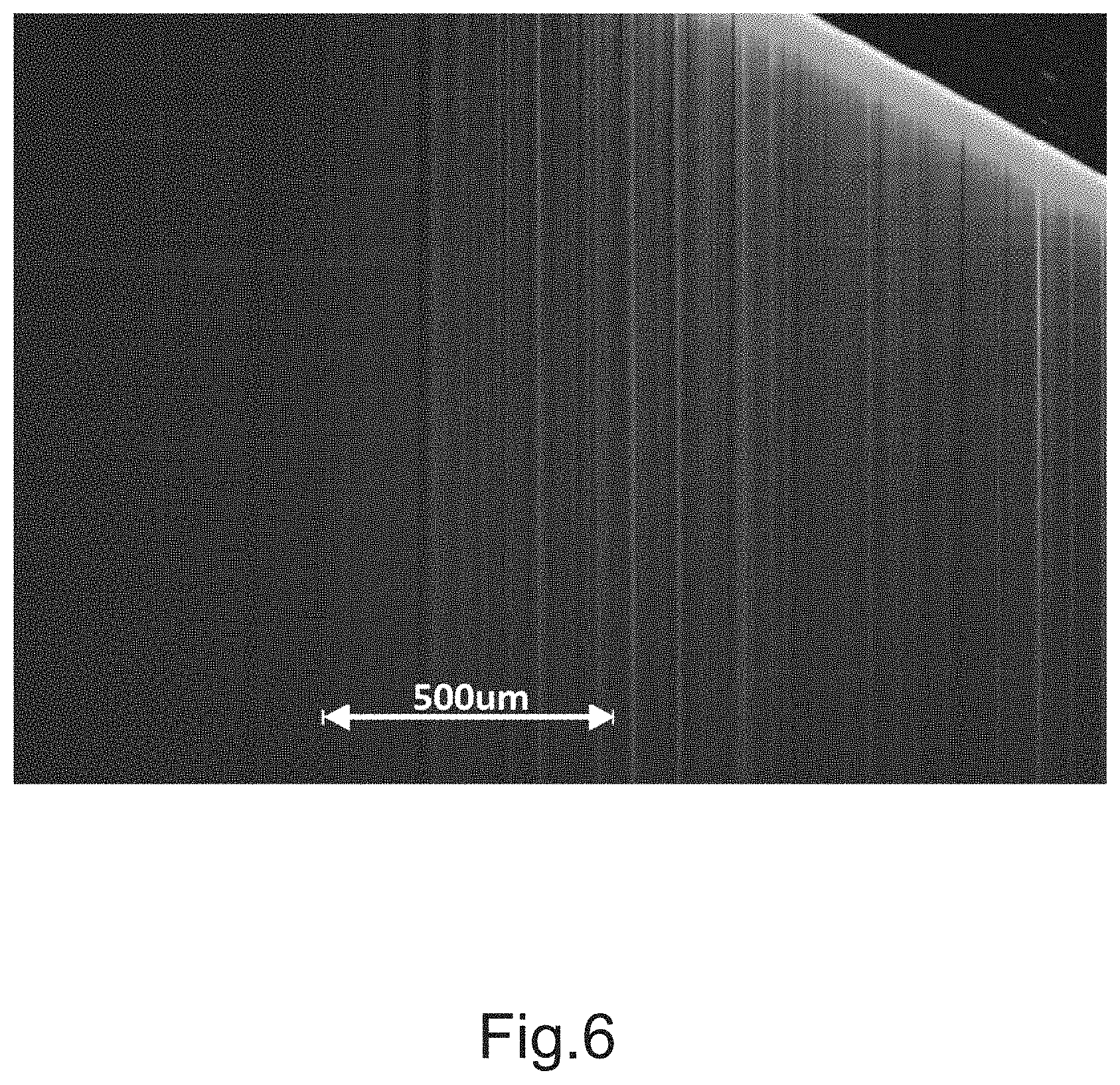
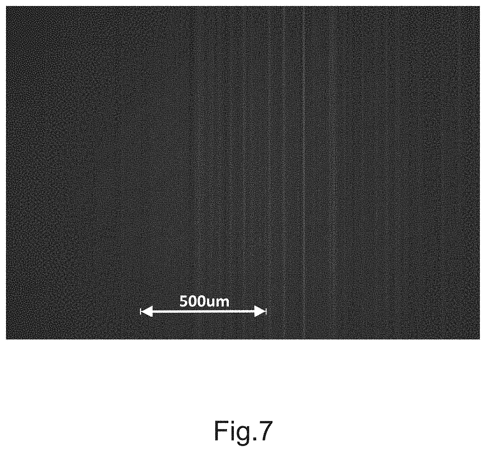
[0009] There is also a more serious and fundamental problem than the resistivity problem. It is a problem of mechanical strength (or heat resistance) of Si itself. Since the difference between the expansion coefficients of LT and Si is extremely large in the LT/Si bonded wafers, if low-temperature heat treatment (e.g., 300.degree. C.) is performed after the bonding, a shift of crystals called slip may occur in the Si substrate or the substrate itself may be cracked. FIGS. 6 and 7 show optical micrographs of the slip produced after heat treatment at 300.degree. C. was performed on a wafer to which an LT (20 .mu.m thick) and a high-resistance (>1000 .OMEGA.cm) FZ wafer (oxygen concentration is less than 1 ppma) were bonded. These photographs were obtained by observing a portion where the LT peeled off after the slip occurred, and FIG. 6 is a photograph in the vicinity of the outer periphery of the substrate, and FIG. 7 is a photograph in the vicinity of 5 mm from the outer periphery of the substrate. When the slip occurs, the LT around the slip peels off, and the substrate may be damaged. This is considered to be a big problem because a low oxygen concentration wafer is used.
[0010] As an important point with respect to the occurrence of the slip, it has been clarified that the yield stress increases by increasing the concentration of oxygen dissolved in the Si wafer to be used, "stickiness" occurs in the Si crystal (see, for example, Non-Patent Document 2), and the slip (dislocation) hardly occurs.
[0011] That is, while it is necessary to reduce dissolved oxygen in order to increase the resistivity in order to suppress the dielectric loss, it is necessary to increase dissolved oxygen in order to suppress the problem of mechanical strength.
[0012] In this specification, the method of measuring dissolved oxygen was based on JEIDA-61-2000, which is a standard measurement method of atomic concentrations of interstitial oxygen using infrared. This technique measures the 1106 cm.sup.-1, which is an absorption peak characteristic of interstitial oxygen. A JIR-6500 Fourier Transform Infrared Spectrometer (FT-IR) manufactured by JEOL Ltd. was used as a measuring device. The obtained absorption coefficient .alpha. multiplied by a coefficient 6.28 is the interstitial oxygen concentration (ppma). In this specification, the interstitial oxygen concentration obtained by this method is simply referred to as "oxygen concentration".
PRIOR ART REFERENCES
Patent Documents
[0013] Patent Document 1: U.S. Pat. No. 6,544,656
Non Patent Documents
[0013] [0014] Non-Patent Document 1: Taiyo Yuden Co., Ltd. "Temperature Compensation Technology for SAW-Duplexer Used in RF Front End of Smartphone", Dempa Shimbun High Technology, November 2012 [0015] Non-Patent Document 2: Edited by the UCS Society for Research on Basic Technology of Semiconductors, "Science of Silicon," Realize Science and Technology Center, Jun. 28, 1996, p. 576-582
SUMMARY OF THE INVENTION
Problems to be Solved by the Invention
[0016] It is an object of the present invention to provide a composite substrate and a method of manufacturing the composite substrate which can maintain high resistance after processing at 300.degree. C.
Means of Solving the Problems
[0017] In order to concurrently solve the problems of dielectric losses and mechanical strength that occur when Si is used as a support substrate, the present inventors have focused on manufacturing processes of LT-SAW devices including LT/Si bonded substrates. SAW devices such as LTs and LT/Si do not require high-temperature processes (e.g., gate-oxidation) like semiconductor CMOS processes, and the maximum temperature is about 300.degree. C. If a high resistance is maintained up to this temperature, no problem arises in terms of characteristics. Therefore, the idea of using a Si substrate capable of maintaining high resistance up to about 300.degree. C. as a support substrate has been reached. From this point of view, it can be said that this purpose is met even if the oxygen concentration is somewhat high. That is, in the application to LT-SAW devices, whether or not the high resistivity can be maintained after processing at 300.degree. C. is a very significant criterion for judging whether or not Si substrate can be adopted.
[0018] In order to solve the above problems, a composite substrate according to the present invention is manufactured by bonding a silicon (Si) wafer having an interstitial oxygen concentration of 2 to 10 ppma as a support substrate to a piezoelectric material substrate, and thinning the piezoelectric material substrate after the bonding.
[0019] In the present invention, the piezoelectric material substrate may be a lithium tantalate wafer (LT) substrate or a lithium niobate (LN) substrate. The silicon wafer may be cut out from a crystal produced by any of the FZ method, the MCZ method, and the CZ method.
[0020] In the present invention, the composite substrate may have an intervening layer between the piezoelectric material substrate and the silicon wafer. The intervening layers may include any of silicon oxide, silicon nitride, silicon oxynitride (SiON), and amorphous silicon. The intervening layer may be thermally oxidized silica. The intervening layer may be formed by chemical vapor deposition (CVD) or physical vapor deposition (PVD), or may be formed by applying a silicone-based oil. When the intervening layer is formed by applying a silicone-based oil, the oil may contain perhydropolysilazane or methyltrimethoxysilane. By providing such an intervening layer, the bonding strength can be increased and peeling can be suppressed.
[0021] In the present invention, one or both of the piezoelectric material substrate and the silicon wafer may be subjected to surface activation treatment before bonding. In this case, the surface activation treatment may be performed using a vacuum ion beam or a plasma activation method. These surface activation treatments can increase the bonding strength.
[0022] In order to solve the above problems, a method of manufacturing a composite substrate according to the present invention includes a step of preparing a piezoelectric material substrate, a step of preparing a silicon (Si) wafer having an interstitial oxygen concentration of 2 to 10 ppma as a support substrate, a step of bonding the piezoelectric material substrate and the silicon wafer, and a step of thinning the piezoelectric material substrate after the bonding step.
[0023] In the present invention, the piezoelectric material substrate may be a lithium tantalate wafer (LT) substrate or a lithium niobate (LN) substrate. The silicon wafer may be cut out from a crystal produced by any of the FZ method, the MCZ method, and the CZ method.
[0024] The present invention may further include a step of providing an intervening layer on either or both of the surface of the piezoelectric material substrate and the silicon wafer prior to the step of bonding. The intervening layer may include any one of a silicon oxide, a silicon nitride, a silicon oxynitride (SiON), and amorphous silicon. In the step of providing the intervening layer, the silicon wafer may be thermally oxidized. In the step of providing the intervening layer, the intervening layer may be formed by chemical vapor deposition (CVD) or physical vapor deposition (PVD). In the step of providing the intervening layer, the intervening layer may be formed by applying a silicone-based oil. In this case, the silicone-based oil may contain perhydropolysilazane or methyltrimethoxysilane.
[0025] The present invention may further include a step of performing surface activation treatment on one or both of the piezoelectric material substrate and the silicon wafer before the step of bonding. The surface activation treatment may be performed using a vacuum ion beam or a plasma activation method. These surface activation treatments can increase the bonding strength.
BRIEF DESCRIPTION OF THE DRAWINGS
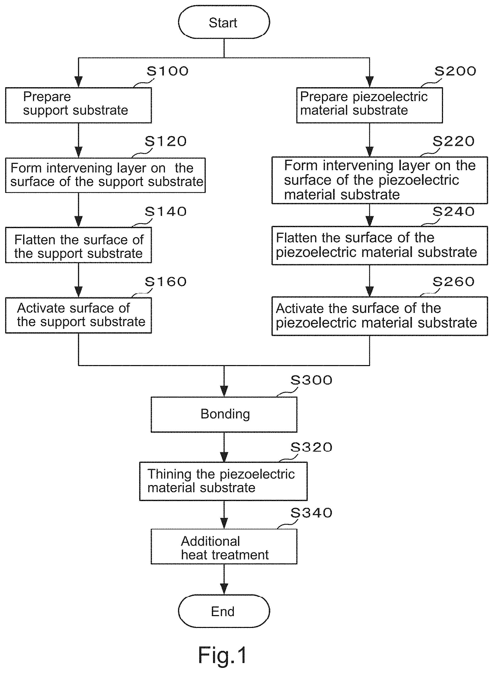
[0026] FIG. 1 is a flowchart of the manufacturing process of the composite substrate according to the present embodiment.
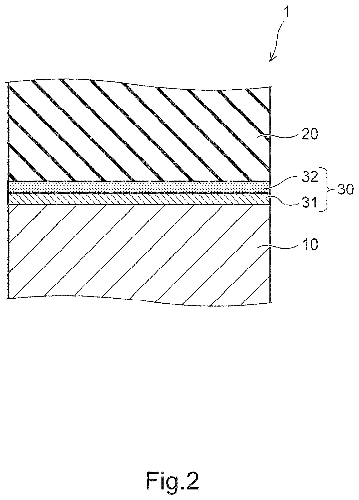
[0027] FIG. 2 is a schematic cross-sectional view illustrating a composite substrate according to the present embodiment.
[0028] FIG. 3 is a graph showing the results of Example 2.
[0029] FIG. 4 is a graph showing the results of Example 3.
[0030] FIG. 5 is a graph showing thermal expansion coefficients of various materials in comparison.
[0031] FIG. 6 is an optical micrograph of a slip generated after heat treatment in the vicinity of the outer periphery of a Si substrate.
[0032] FIG. 7 is an optical micrograph of a slip generated after heat treatment in the vicinity of 5 mm from the outer periphery of the Si substrate.
DESCRIPTION OF EMBODIMENTS
[0033] The composite substrate 1 of the present embodiment is manufactured through a process in which the support substrate 10 and the piezoelectric material substrate 20 are respectively subjected to processing before bonding as necessary, and then the substrates are bonded together. Hereinafter, the manufacturing method will be described with reference to the flowchart shown in FIG. 1.
[0034] [Treatment of Support Substrate]
[0035] First, support substrate 10 is prepared (step S100). As the support substrate 10, a silicon (Si) wafer having an interstitial oxygen concentration of 2 to 10 ppma is used. The Si wafer used as the support substrate 10 is cut out from a single crystal ingot of Si manufactured by the FZ method, the MCZ method, or the CZ method.
[0036] Next, as required, intervening layer 31 is formed on the surface of the support substrates 10 (step S120). The material of the intervening layer 31 may include any of a silicon oxide, a silicon nitride, silicon oxynitride (SiON), and amorphous silicon. The intervening layer 31 can be formed, for example, as a film of thermally oxidized silica obtained by thermally oxidizing a Si wafer. Thermally oxidized silica is grown at a high temperature, so that it is dense, has few impurities, and can absorb a certain amount of gas. The intervening layer 31 may be formed by other methods. For example, the intervening layer 31 may be formed of a material suitable as an intervening layer by chemical vapor deposition (CVD) such as plasma enhanced CVD (Chemical Vapor Deposition). The intervening layer 31 may be formed of a material suitable for the intervening layer by physical vapor deposition (PVD). Alternatively, the intervening layer 31 may be formed by applying a silicone-based oil. The silicone based oil to be applied may contain perhydropolysilazane or methyltrimethoxysilane. The silicone-based oil may be applied by spin coating.
[0037] Subsequently, the surface of the support substrate 10 to be bonded to the piezoelectric material substrate 20 is flattened as required (step S140). The degree of flattening is preferably such that the surface roughness is 0.3 nm or less in Ra. The flattening may be performed by chemical mechanical polishing. When the intervening layer 31 is not provided on the support substrate 10, the support substrate 10 itself is flattened. When the intervening layer 31 is provided on the support substrate 10, the surface of the intervening layer 31 is flattened. When the intervening layer 31 is provided, the characteristics of the composite substrate 1 do not depend on the initial surface roughness of the support substrate 10 to be a base. For example, the initial surface roughness of the support substrate 10 may be 150 nm or more in Ra.
[0038] In addition, as described as "if necessary", when a sufficiently flat surface is obtained without the flattening step, the flattening step may be omitted. For example, when the intervening layer 31 is formed by thermal oxidation using the support substrate 10 whose surface is finished as a mirror surface, the surface of the intervening layer 31 also becomes a mirror surface like the base, and therefore this flattening step is unnecessary.
[0039] Further, in order to increase the bonding strength at the time of bonding, an activation treatment is performed on the surface to be bonded (i.e., the surface of the support substrate 10 when the intervening layer 31 is not provided, or the surface of the intervening layer 31 when the intervening layer 31 is provided) as required (step S160). The surface activation treatment may be, for example, any of ozone water treatment, UV ozone treatment, ion beam treatment, and plasma treatment.
[0040] As described above, the processing before bonding to the support substrate 10 is completed.
[Processing of Piezoelectric Material Substrate]
[0041] First, the piezoelectric material substrate 20 is prepared (step S200). The piezoelectric material substrate 20 is a substrate of a piezoelectric material such as lithium tantalate (LT) or lithium niobate (LN), and is preferably a single crystal substrate of these piezoelectric material.
[0042] Next, as required, intervening layer 32 is formed on the surface of the piezoelectric material substrates 20 (step S220). The material of the intervening layer 32 may include any of a silicon oxide, a silicon nitride, silicon oxynitride (SiON), and amorphous silicon. The intervening layer 32 can be formed by the following method. That is, the intervening layer 32 may be formed by depositing a suitable material as the intervening layer by chemical vapor deposition (CVD) such as plasma CVD. The intervening layer 32 may be formed by depositing a suitable material as the intervening layer by physical vapor deposition (PVD). Alternatively, the intervening layer 32 may be formed by applying a silicone-based oil. The silicone based oil to be applied may contain perhydropolysilazane or methyltrimethoxysilane. The silicone-based oil may be applied by spin coating.
[0043] Subsequently, the surfaces to be bonded to the support substrate 10 is flattened as required (step S240). The degree of flattening is preferably such that the surface roughness is 0.3 nm or less in Ra (arithmetic mean roughness). The flattening may be performed by chemical mechanical polishing. When the intervening layer 32 is not provided on the piezoelectric material substrate 20, the piezoelectric material substrate 20 itself is flattened. When the intervening layer 32 is provided on the piezoelectric material substrate 20, the surface of the intervening layer 32 is flattened. When the intervening layer 32 is provided, the characteristics of the composite substrate 1 do not depend on the initial surface roughness of the piezoelectric material substrate 20 to be a base. For example, the initial surface roughness of the piezoelectric material substrate 20 may be 150 nm or more in Ra.
[0044] Further, in order to increase the bonding strength at the time of bonding, an activation treatment is performed on the surface to be bonded (i.e., the surface of the piezoelectric material substrate 20 when the intervening layer 32 is not provided, or the surface of the intervening layer 32 when the intervening layer 31 is provided) as required (step S260). The surface activation treatment may be, for example, ozone water treatment, UV ozone treatment, ion beam treatment (e.g., vacuum ion beam treatment), or plasma treatment.
[0045] As described above, the processing before the bonding to the piezoelectric material substrate 20 is completed.
[Pasting and Subsequent Processing]
[0046] The support substrate 10 and the piezoelectric material substrate 20 treated as described above are bonded to each other (step S300). In this case, the bonding strength may be increased by heating to a low temperature. The heating temperature at this low temperature may be, for example, about 100.degree. C., and the heating time may be about 24 hours.
[0047] Subsequently, if desired, the piezoelectric material substrate 20 is grinded and polished to be thinned (step S320). For example, the thickness of the piezoelectric material substrate 20 is reduced to about 20 .mu.m. Additional heat treatment may then be performed as required to enhance the bonding (step S340).
[0048] According to the manufacturing method described above, the composite substrate 1 in which the piezoelectric material substrate 20 and the support substrate 10 are bonded to each other can be manufactured. FIG. 2 is a schematic cross-sectional view of the composite substrate 1 according to the present embodiment. In the composite substrate 1, the intervening layer 31 provided on the support substrate 10 and/or the intervening layer 32 provided on the piezoelectric material substrate 20 become the intervening layer 30 sandwiched between the piezoelectric material substrate 20 and the support substrate 10.
EXAMPLES
[0049] Hereinafter, examples performed to confirm the effects of the present invention will be described. Although examples in which a lithium tantalate (LT) wafer is mainly used as the piezoelectric material substrate are described, the same effect can be obtained by using a lithium niobate (LN) wafer instead of the LT wafer.
Example 1
[0050] Ten types of 150 mm .PHI. Si wafers (thickness: 625 .mu.m, P-type, resistivity: around 1100 .OMEGA.cm) were prepared, and 150 mm .PHI. LT wafers (thickness: 250 .mu.m) were bonded together. Table 1 shows the manufacturing method of the single crystal ingot and the oxygen concentration of each of the 10 types of prepared Si wafers. Note that the type of the wafer is represented by a combination of a method for manufacturing a single crystal ingot and a numerical value of an oxygen concentration. For example, 1 ppma wafers produced by the FZ-method were described as "FZ1".
TABLE-US-00001 TABLE 1 Wafer type FZ0 FZ1 FZ2 MCZ2 MCZ5 MCZ10 MCZ12 CZ10 CZ12 CZ15 Method of FZ FZ FZ MCZ MCZ MCZ MCZ CZ CZ CZ manufacturing ingot Oxygen ~0 1 2 2 5 10 12 10 12 15 concentration (ppma)
[0051] It was confirmed that the surface roughness of each of the Si wafer and the LT wafer to be bonded was 0.3 nm or less in Ra (arithmetic mean roughness) The bonding was performed by a room temperature bonding method using a vacuum ion beam. After bonding, the LT wafer was thinned to 20 .mu.m by grinding and polishing. The wafer of the composite substrate thus bonded was reciprocated 10 times between a hot plate at 300.degree. C. and a cooling stage, and thereafter, the occurrence of the slip and the state of cracking of the wafer were observed. The test results are shown in Table 2. From these results, it was found that the generation of the slip and wafer cracking can be prevented if the oxygen concentration of the Si wafer is 2 ppma or more. Similar results were obtained when LN was used instead of LT in the same experiment.
TABLE-US-00002 TABLE 2 Wafer type FZ0 FZ1 FZ2 MCZ2 MCZ5 MCZ10 MCZ12 CZ10 CZ12 CZ15 Slip 2nd 6th None None None None None None None None occrrence time time Wafer 9th 6th None None None None None None None None cracking time time
Example 2
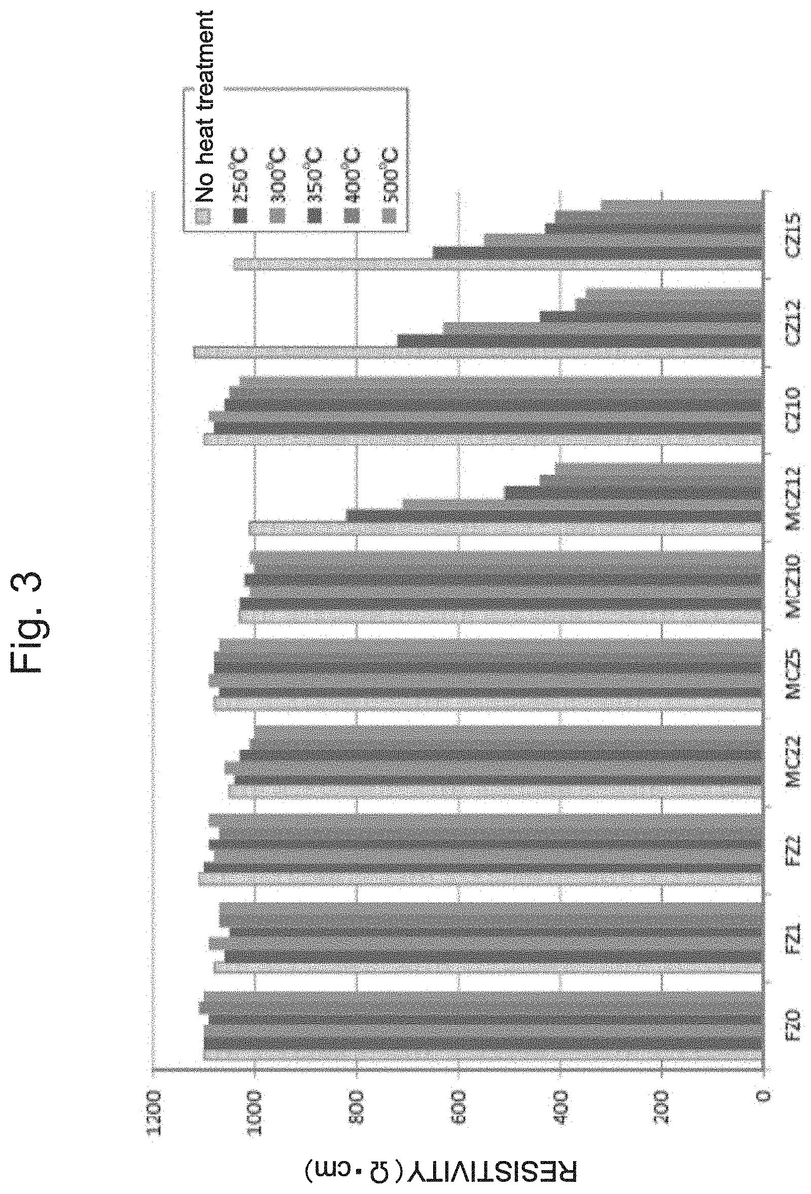
[0052] Ten types of Si wafers were prepared in the same manner as in Example 1, and heat treatment was performed at 250.degree. C., 300.degree. C., 350.degree. C., 400.degree. C., 450.degree. C., and 500.degree. C. for 1 hour in a nitrogen atmosphere. The results of measurement of resistivity before and after heat treatment are shown in Table 3 and FIG. 3. As a result, it was found that, when the oxygen concentration of the Si wafer was 10 ppma or less, there was little change in resistivity even when heat treatment was performed up to 350.degree. C., which is considered to be the maximum temperature of the LT device manufacturing process, regardless of the manufacturing method of the Si single crystal ingot.
TABLE-US-00003 TABLE 3 Wafer type FZ0 FZ1 FZ2 MCZ2 MCZ5 MCZ10 MCZ12 CZ10 CZ12 CZ15 No heat treatment 1100 1080 1110 1050 1080 1030 1010 1100 1120 1040 250.degree. C. 1100 1060 1100 1040 1070 1030 820 1080 720 650 300.degree. C. 1100 1090 1080 1060 1090 1010 710 1090 630 550 350.degree. C. 1090 1050 1090 1030 1080 1020 510 1060 440 430 400.degree. C. 1110 1070 1070 1010 1080 1000 440 1050 370 410 500.degree. C. 1100 1070 1090 1000 1070 1010 410 1030 350 320
Example 3
[0053] A resonator was produced using the wafers of the 10 kinds of composite substrates obtained in Example 1, and the Q factor was measured. The maximum temperature of the manufacturing process of the resonator, which is an LT device, is about 350.degree. C. For broken wafers, devices are manufactured and measured using surviving portion (i.e., a portion having a size sufficient for manufacturing a device), and for slipped wafers, devices are manufactured and measured using non-slipped portion. The measurement results of the Q factors are shown in Table 4 and FIG. 4. From this result, no deterioration in characteristics was observed for Si wafers having an oxygen concentration of 10 ppma or less, and deterioration in characteristics was observed for Si wafers having an oxygen concentration greater than 10 ppma. This result was found to be consistent with the change in resistivity in Example 2.
TABLE-US-00004 TABLE 4 Wafer type FZ0 FZ1 FZ2 MCZ2 MCZ5 MCZ10 MCZ12 CZ10 CZ12 CZ15 Q factor 2500 2510 2500 2520 2480 2510 2010 2470 2070 1720
Example 4
[0054] Ten types of 150 mm .PHI. Si wafers having a thickness of 625 .mu.m were prepared in the same manner as in Example 1, and a thermal oxide film having a thickness of 100 nm was grown. The thermal oxidation conditions are input at 700.degree. C. and dry oxidation at 1000.degree. C. LT wafers having a thickness of 250 .mu.m and a diameter of 150 mm.PHI. was prepared. Surface activation was performed on both the Si wafer on which the thermal oxide film was grown and the LT wafer by plasma activation, and both wafers were bonded to each other. After the bonding, heat treatment was performed at 100.degree. C. for 24 hours. It was confirmed that the surface roughness of each wafer before bonding was 0.3 nm or less in Ra.
[0055] After bonding and heat treatment, the LT wafer was thinned to 20 .mu.m by grinding and polishing. These wafers were reciprocated 10 times between a hot plate at 300.degree. C. and a cooling stage, and then slip generation and crack state of the wafers were observed. The results are provided in Table 5. From this result, it was found that the generation of the slip and the cracking of the wafer can be prevented if the oxygen concentration of the Si wafer is equal to or higher than the 2 ppma oxygen concentration. This result was almost the same as that of Example 1 embodiment, and it was found that generation of the slip and wafer cracking depend on the oxygen concentration of the Si wafer regardless of the presence or absence of the thermal oxide film, and that it is important that the oxygen concentration is 2 ppma or more.
TABLE-US-00005 TABLE 5 Wafer type FZ0 FZ1 FZ2 MCZ2 MCZ5 MCZ10 MCZ12 CZ10 CZ12 CZ15 Slip 4th 8th None None None None None None None None occurrence time time Wafer 8th 10th None None None None None None None None cracking time time
Example 5
[0056] Ten types of Si wafers were prepared in the same manner as in Example 1, and thermal oxidation was performed in the same manner as in Example 4. With respect to the Si wafer provided with the thermal oxide film in this manner, the conditions of the additional heat treatment were changed, and the resistivity before and after the additional heat treatment was measured. The conditions of the additional heat treatment were six types, i.e., no additional heat treatment, 250.degree. C., 300.degree. C., 350.degree. C., 400.degree. C., and 500.degree. C., and the additional heat treatment was performed in a nitrogen atmosphere for 1 hour. The resistivity was measured before and after the additional heat treatment. The result of the measurement was almost the same as that of Example 2, and it was found that, when the oxygen concentration was 10 ppma or less, there was almost no change in resistivity even when heat treatment was performed up to 350.degree. C. It has been found that even when a Si wafer provided with a thermal oxide film is used, it can be used without problems such as a decrease in resistivity by avoiding the treatment in the thermal donor generation temperature range (400 to 600.degree. C.).
Example 6
[0057] Ten types of 150 mm m Si wafers having a thickness of 625 .mu.m were prepared in the same manner as in Example 1, and a plasma CVD oxide film having a thickness of 200 nm was deposited around room temperature. After the oxide film was deposited, polishing for mirroring was performed. LT wafers having a thickness of 250 .mu.m and a diameter of 150 mm.PHI. was prepared. Surface activation was performed on both the Si wafer on which the oxide film was deposited and the LT wafer by plasma activation, and both wafers were bonded to each other. After the bonding, heat treatment was performed at 100.degree. C. for 24 hours. It was confirmed that the surface roughness of both wafers before bonding was 0.3 nm or less in Ra. As a result of conducting the same heat resistance experiment as in Example 1, the same tendency as in Example 1 was exhibited. From this result, it was found that the effect of the present invention can be obtained without depending on the method of forming the oxide film.
Example 7
[0058] Ten types of 150 mm m Si wafers (thickness: 625 .mu.m) and 150 mm .PHI. LT wafers (thickness: 250 .mu.m) were prepared in the same manner as in Example 1, and a plasma CVD oxide film of 200 nm was deposited on the LT wafer in the vicinity of room temperature. After deposition, polishing for mirroring was performed. Both the Si wafer and the LT wafer on which the oxide film was deposited were subjected to surface activation by plasma activation, and both wafers were bonded to each other. After the bonding, heat treatment was performed at 100.degree. C. for 24 hours. It was confirmed that the surface roughness of both wafers before bonding was 0.3 nm or less in Ra. The same heat resistance experiment as in Example 1 was performed, and the results showed exactly the same tendency as in Example 1. From this result, it was found that the effect of the present invention can be obtained regardless of the position where the oxide film is formed, i.e., whether the intervening layer such as the oxide film is provided on the Si wafer or the LT wafer.
Example 8
[0059] Ten types of 150 mm .PHI. Si wafers (thickness: 625 .mu.m) and 150 mm .PHI. LT wafers (thickness: 250 .mu.m) with rough surfaces (Ra=160 nm) were prepared in the same manner as in Example 1, and 5 .mu.m plasma CVD oxide films were deposited on the LT wafers around room temperature. After deposition, polishing for mirroring was performed. Both the Si wafer and the LT wafer on which the oxide film was deposited were subjected to surface activation by plasma activation, and both wafers were bonded to each other. After the bonding, heat treatment was performed at 100.degree. C. for 24 hours. It was confirmed that the surface roughness of both wafers before bonding was 0.3 nm or less in Ra. The results showed exactly the same trend as in Example 1. From this result, it was found that the effect of the present invention can be obtained regardless of the initial surface roughness of the LT wafer forming the intervening layer. In the same manner, the same results as in Example 1 were obtained when Si (Ra=175 nm) having a rough surface was used and the same experiment was carried out. In addition, the same results were obtained when intervening layers were provided on a surface where both the LT and Si bonded surfaces were rough. Therefore, it has been found that in the case where an intervening layer is provided between LT and Si, the effect of the present method is not affected even if one or both of the bonded surfaces of LT or Si are not mirror-polished.
Example 9
[0060] Ten types of 150 mm m Si wafers (thickness: 625 .mu.m) were prepared in the same manner as in Example 1, and 200 nm plasma CVD nitrided (SiN) film was deposited at around room temperature. After deposition, polishing for mirroring was performed. LT wafers having a thickness of 250 .mu.m and a diameter of 150 mm.PHI. was prepared. Surface activation was performed on both the Si wafer on which the nitride film was deposited and the LT wafer by plasma activation, and both wafers were bonded to each other. After the bonding, heat treatment was performed at 100.degree. C. for 24 hours. It was confirmed that the surface roughness of both wafers before bonding was 0.3 nm or less in Ra. The results showed exactly the same trend as in Example 1. It has been found that this method does not depend on the method of forming the oxide film. Similar results were also obtained when amorphous Si (formed by physical vapor deposition (PVD)), SiON, or the like was deposited on Si wafers. From these results, it has been found that the effect of the present invention can be obtained regardless of the type (material) of the intervening layer. The same result was obtained when the silicon oxide film was formed by spin coating a silicone oil such as perhydropolysilazane or methyltrimethoxysilane.
[0061] From the above results, it was found that high mechanical strength and heat resistance (slip resistance and substrate crack resistance) can be achieved by using a Si wafer having an interstitial oxygen concentration of 2 to 10 ppma as a support substrate, and at the same time, deterioration of device characteristics (Q factor) due to dielectric loss can be prevented. It has also been found that there is no dependence on the presence or absence, the type of the intervening layer, the initial surface roughness of the substrate, and the like. Since the Si wafer produced by the CZ method can also be used as a support substrate, it has been found that the problems of mechanical strength and dielectric loss can be solved and low cost can be achieved at the same time.
[0062] Although the present embodiment has been described above, the present invention is not limited to these examples. For example, anything obtained by appropriately performing addition, removal or design alteration of a component with respect to the embodiments described above by a person skilled in the art or appropriate combination of the features of each embodiment is included in the range of the present invention as long as containing a gist of the present invention.
REFERENCE SIGNS LIST
[0063] 1 Composite substrate [0064] 10 Support substrate [0065] 20 Piezoelectric material substrate [0066] 30, 31, 32 Intervening layer
* * * * *
D00000
D00001
D00002
D00003
D00004
D00005
D00006
D00007
XML
uspto.report is an independent third-party trademark research tool that is not affiliated, endorsed, or sponsored by the United States Patent and Trademark Office (USPTO) or any other governmental organization. The information provided by uspto.report is based on publicly available data at the time of writing and is intended for informational purposes only.
While we strive to provide accurate and up-to-date information, we do not guarantee the accuracy, completeness, reliability, or suitability of the information displayed on this site. The use of this site is at your own risk. Any reliance you place on such information is therefore strictly at your own risk.
All official trademark data, including owner information, should be verified by visiting the official USPTO website at www.uspto.gov. This site is not intended to replace professional legal advice and should not be used as a substitute for consulting with a legal professional who is knowledgeable about trademark law.