Optical Wireless Communication System
Hsiang; Jui-Chieh ; et al.
U.S. patent application number 16/114223 was filed with the patent office on 2019-11-28 for optical wireless communication system. The applicant listed for this patent is ACER INCORPORATED. Invention is credited to Chih-Chiang Chen, Jui-Chieh Hsiang.
| Application Number | 20190363790 16/114223 |
| Document ID | / |
| Family ID | 67764595 |
| Filed Date | 2019-11-28 |


| United States Patent Application | 20190363790 |
| Kind Code | A1 |
| Hsiang; Jui-Chieh ; et al. | November 28, 2019 |
OPTICAL WIRELESS COMMUNICATION SYSTEM
Abstract
An optical wireless communication system includes a display panel, a frame rate controller, a backlight module, and a timing controller. The display panel includes a glass substrate, and the frame rate controller is configured to modulate multiple frequencies. The timing controller is configured to drive different scan regions of the glass substrate using at least a first frequency and a second frequency among the multiple frequencies and/or drive different backlight regions of the backlight module using at least a third frequency and a fourth frequency among the multiple frequencies for transmitting optical data. The first frequency is different from the second frequency, the third frequency is different from the fourth frequency, the value of the second frequency is a multiple of the value of the first frequency, and the value of the fourth frequency is a multiple of the value of the third frequency.
| Inventors: | Hsiang; Jui-Chieh; (New Taipei City, TW) ; Chen; Chih-Chiang; (New Taipei City, TW) | ||||||||||
| Applicant: |
|
||||||||||
|---|---|---|---|---|---|---|---|---|---|---|---|
| Family ID: | 67764595 | ||||||||||
| Appl. No.: | 16/114223 | ||||||||||
| Filed: | August 28, 2018 |
| Current U.S. Class: | 1/1 |
| Current CPC Class: | H04B 10/1141 20130101; H04B 10/502 20130101; H04B 10/116 20130101 |
| International Class: | H04B 10/116 20060101 H04B010/116; H04B 10/50 20060101 H04B010/50; H04B 10/114 20060101 H04B010/114 |
Foreign Application Data
| Date | Code | Application Number |
|---|---|---|
| May 28, 2018 | TW | 107118080 |
Claims
1. An optical wireless communication system, comprising: a display panel including a glass substrate; a backlight module configured to provide light for operating the display panel; a frame rate controller configured to modulate multiple frequencies; a scan driving circuit; and a timing controller configured to: instruct the scan driving circuit to drive a first scan region and a second scan region of the glass substrate using at least a first frequency and a second frequency among the multiple frequencies so as to transmit an optical data; and instruct the backlight module to drive a first backlight region of the backlight module using a third frequency and drive a second backlight region of the backlight module using a fourth frequency, wherein the first frequency is different from the second frequency, the third frequency id different from the fourth frequency, a value of the second frequency is a multiple of a value of the first frequency, and a value of the fourth frequency is a multiple of a value of the third frequency.
2. The optical wireless communication system of claim 1, wherein the scan driving circuit comprises: a first integrated circuit configured to refresh images of the first scan region using the first frequency so as to transmit the optical data; and a second integrated circuit configured to refresh images of the second scan region using the second frequency so as to transmit the optical data.
3. (canceled)
4. The optical wireless communication system of claim 1, wherein the frame rate controller is disposed on a graphics processing unit terminal, and the timing controller, the scan driving circuit and the display panel are disposed on a panel control terminal.
5. The optical wireless communication system of claim 1, wherein the frame rate controller, the timing controller, the scan driving circuit and the display panel are disposed on a panel control terminal.
6. (canceled)
Description
CROSS REFERENCE TO RELATED APPLICATION
[0001] This application claims priority of Taiwan Application No. 107118080 filed on May 28, 2018.
BACKGROUND OF THE INVENTION
1. Field of the Invention
[0002] The present invention is related to an optical wireless communication system, and more particularly, to an optical wireless communication system with low power consumption, high data capacity and low image flicker.
2. Description of the Prior Art
[0003] Compared to traditional incandescent bulbs, light-emitting diodes (LEDs) are advantageous in low power consumption, long lifetime, small size, no warm-up time, fast reaction speed, and the ability to be manufactured as small or array devices. In addition to outdoor displays, traffic signs, and liquid crystal display (LCD) backlight for various electronic devices such as mobile phones, notebook computers or personal digital assistants (PDAs), LEDs are also widely used as indoor/outdoor lighting devices in place of fluorescent of incandescent lamps.
[0004] With the development in global communication, optical wireless communication technologies proliferate and become essential in deploying communication networks. An optical wireless communication system may take advantage of LEDs which can be pulsed at very high speeds without noticeable effect on the lighting output and human eyes, thereby transmitting optical date. In addition to high data capacity, a visible light optical wireless communication can provide more secure communications over a radio wave wireless system by using narrow and highly-directional beams for data transmission. Also, the operation of the visible light optical wireless communication does not pose hazards to human bodies or interfere with surrounding equipment, and can function as a secure wireless base station.
[0005] Existing optical wireless communication systems adopt an LED backlight signal modulation scheme in which a transmitting display is configured to transmit fast-pulsed digital signals (logic 1 and logic 0) by adjusting the refresh frequency of a backlight module, while a receiving device is configured to receive and identify the digital signals unperceivable to human eyes using an image sensor equipped with a specific application program. However, the above-mentioned backlight signal modulation scheme operates at high frequencies which may increase the power consumption of the backlight module and reduce image brightness. When required to operate in a low-brightness backlight mode, the backlight module may not be able to adjust the brightness of an image to a designated low value when implemented with the backlight signal modulation scheme. Therefore, there is a need for to an optical wireless communication system with low power consumption and high data capacity.
SUMMARY OF THE INVENTION
[0006] The present invention provides an optical wireless communication system which includes a display panel, a frame rate controller, a scan driver and a timing controller. The display panel includes a glass substrate. The frame rate controller is configured to modulate multiple frequencies. The timing controller is configured to instruct the scan driving circuit to drive a first scan region and a second scan region of the glass substrate using at least a first frequency and a second frequency among the multiple frequencies so as to transmit an optical data. The first frequency is different from the second frequency, and a value of the second frequency is a multiple of a value of the first frequency.
[0007] The present invention also provides an optical wireless communication system which includes a display panel, a backlight module, a frame rate controller, and a timing controller. The backlight module is configured to provide light for operating the display panel. The frame rate controller is configured to modulate multiple frequencies. The timing controller is configured to instruct the backlight module to drive a first backlight region of the backlight module using at least a first frequency among the multiple frequencies and drive a second backlight region of the backlight module using at least a second frequency. The first frequency is different from the second frequency, and a value of the second frequency is a multiple of a value of the first frequency.
[0008] These and other objectives of the present invention will no doubt become obvious to those of ordinary skill in the art after reading the following detailed description of the preferred embodiment that is illustrated in the various figures and drawings.
BRIEF DESCRIPTION OF THE DRAWINGS
[0009] FIG. 1 is a functional diagram illustrating an optical wireless communication system according to an embodiment of the present invention.
[0010] FIG. 2 is a functional diagram illustrating an optical wireless communication system according to another embodiment of the present invention.
[0011] FIG. 3 is a diagram illustrating a method of performing optical wireless communication according to an embodiment of the present invention.
[0012] FIG. 4 is a diagram illustrating a method of performing optical wireless communication according to another embodiment of the present invention.
[0013] FIG. 5 is a diagram illustrating a method of performing optical wireless communication according to another embodiment of the present invention.
[0014] FIG. 6 is a diagram illustrating a method of performing optical wireless communication according to another embodiment of the present invention.
DETAILED DESCRIPTION
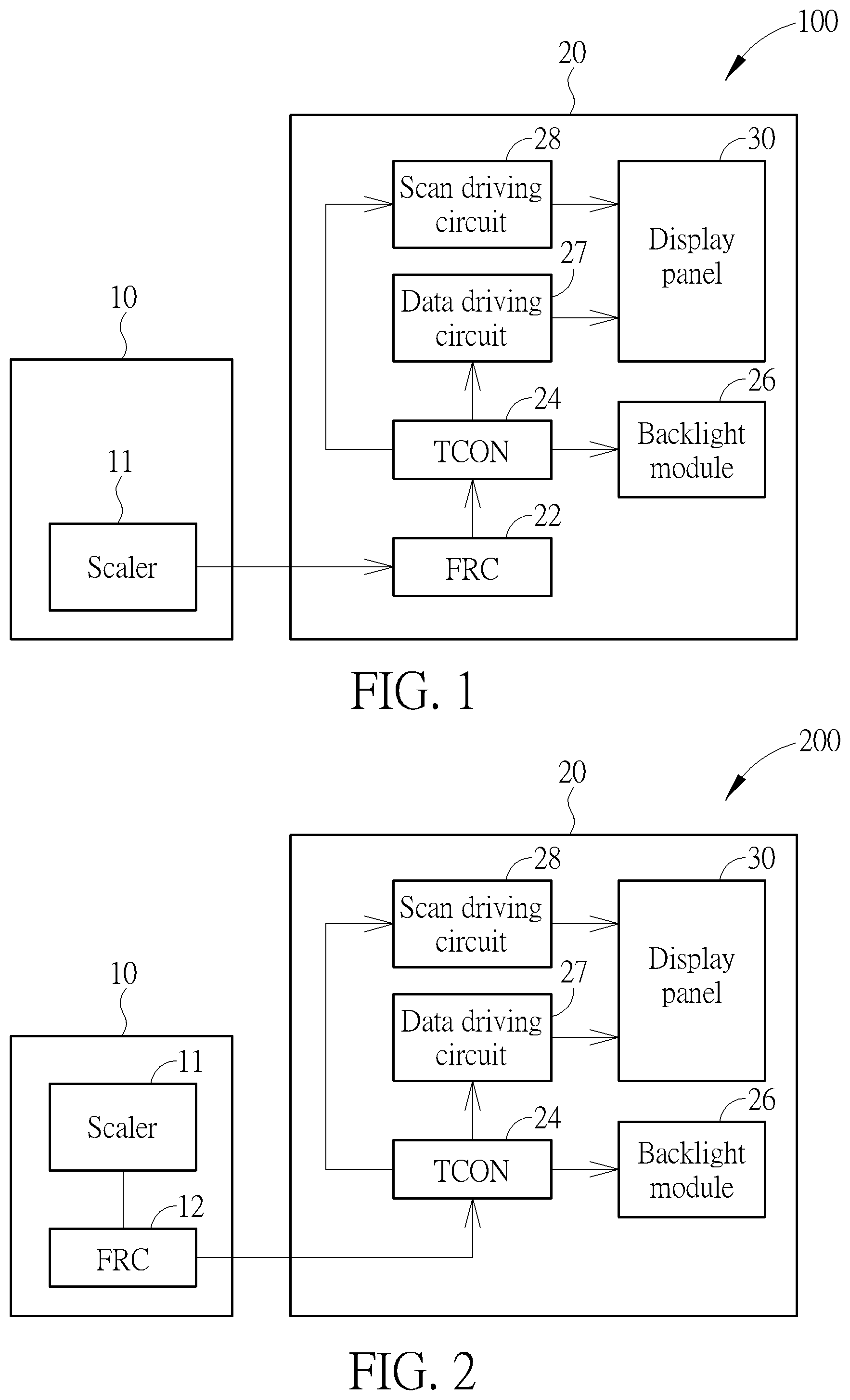
[0015] FIG. 1 is a functional diagram illustrating an optical wireless communication system 100 according to an embodiment of the present invention. FIG. 2 is a functional diagram illustrating an optical wireless communication system 200 according to another embodiment of the present invention. Each of the optical wireless communication systems 100 and 200 includes a graphics processing unit (GPU) terminal 10 and a panel control panel 20. In the optical wireless communication system 100, the GPU terminal 10 includes a scaler 11, while the panel control panel 20 includes a frame rate controller (FRC) 22, a timing controller (TCON) 24, a backlight module 26, a data driving circuit 27, a scan driving circuit 28, and a display panel 30. In the optical wireless communication system 200, the GPU terminal 10 includes a scaler 11 and a frame rate controller 12, while the panel control panel 20 includes a timing controller 24, a backlight module 26, a data driving circuit 27, a scan driving circuit 28, and a display panel 30.
[0016] In an embodiment of the present invention, the backlight module 26 may include multiple LEDs in order to provide the light for operating the display panel 30. The display panel 30 may be a liquid crystal display (LCD) panel which includes a liquid crystal layer, glass substrates, polarizers, filters, and diffuser films. The liquid crystal layer is disposed between two glass substrates. Micro-structures of red, green, blue and black colors are fabricated on the surface of the upper glass substrate so as to form color filters. A plurality of transistors are fabricated on the surface of the lower glass substrate so as to form various driving circuits such as the data driving circuit 27 and the scan driving circuit 28. The current flowing through the transistors by applying different bias voltages results in a variation in electrical field. The rotation angle of the liquid crystal molecules may thus be adjusted for changing the polarity of light, thereby controlling the display of images. However, the structure of the display panel 30 does not limit the scope of the present invention.
[0017] In an embodiment of the present invention, a glass substrate signal frequency modulation scheme may be adopted when performing optical wireless communication. At least two different frequencies are modulated for two different signals. Different scan regions of the glass substrates in the display panel 30 are driven by at least two different frequencies for transmitting optical signals, wherein the value of each frequency among the different frequencies is a multiple of the value of another frequency among the different frequencies.
[0018] FIG. 3 is a diagram illustrating a method of performing optical wireless communication according to an embodiment of the present invention. When transmitting digital optical signals, the frame rate controller 12 or 22 is configured to modulate multiple frequencies so that the timing controller 24 may instruct M integrated circuits IC.sub.1.about.IC.sub.M in the scan driving circuit 28 to drive M scan region SCAN.sub.1.about.SCAN.sub.M of the glass substrates in the display panel 30 using frequencies F.sub.1.about.F.sub.M, respectively. The values of the frequencies F.sub.1.about.F.sub.M have a relationship of F.sub.M=A.sub.i*F.sub.i, wherein M is an integer larger than 1, i is an integer between 0 and M, A.sub.1.about.A.sub.i are positive integers, and at least one of A.sub.1.about.A.sub.i is larger than 1. FIG. 3 depicts an embodiment of M=4 in which the scan driving circuit 28 includes 4 integrated circuits IC.sub.1.about.IC.sub.4 corresponding to the scan region SCAN.sub.1.about.SCAN.sub.4 of the glass substrates in the display panel 30, respectively. The integrated circuit IC.sub.1 is configured to drive the scan region SCAN.sub.1 with an image refresh frequency F.sub.1=30 Hz. The integrated circuit IC.sub.2 is configured to drive the scan region SCAN.sub.2 with an image refresh frequency F.sub.2=60 Hz. The integrated circuit IC.sub.3 is configured to drive the scan region SCAN.sub.3 with an image refresh frequency F.sub.3=120 Hz. The integrated circuit IC.sub.4 is configured to drive the scan region SCAN.sub.4 with an image refresh frequency F.sub.4=240 Hz. In other words, A.sub.1=8, A.sub.2=4, and A.sub.3=2.
[0019] In another embodiment of the present invention, a backlight module frequency modulation scheme may further be adopted when performing optical wireless communication. At least two different frequencies are modulated for two different signals. Different backlight regions of the backlight module 26 are driven by at least two different frequencies for transmitting optical signals, wherein the value of each frequency among the different frequencies is a multiple of the value of another frequency among the different frequencies.
[0020] FIGS. 4.about.6 are diagrams illustrating methods of performing optical wireless communication according to embodiments of the present invention. The backlight module 26 includes N backlight regions BL.sub.1.about.BL.sub.N with refresh frequencies F.sub.BL1.about.F.sub.BLN, respectively. The values of the frequencies F.sub.BL1.about.F.sub.BLN have a relationship of F.sub.BLN=B.sub.j*F.sub.BLj, wherein N is an integer larger than 1, j is an integer between 0 and N, B.sub.1.about.B.sub.j are positive integers, and at least one of B.sub.1.about.B.sub.j is larger than 1. FIGS. 4.about.6 depict the embodiments of N=4 in which the backlight module 26 includes 4 backlight regions BL.sub.1.about.BL.sub.4 with refresh frequencies F.sub.BL1.about.F.sub.BL4. The refresh frequencies F.sub.BL1 of the backlight region BL.sub.1 is 10 MHz. The refresh frequencies F.sub.BL2 of the backlight region BL.sub.2 is 20 MHz. The refresh frequencies F.sub.BL3 of the backlight region BL.sub.3 is 30 MHz. The refresh frequencies F.sub.BL4 of the backlight region BL.sub.4 is 80 MHz. In other words, B.sub.1=8, B.sub.2=4, and B.sub.3=2.
[0021] In another embodiment of the present invention, the backlight regions BL.sub.1.about.BL.sub.N may be vertically-striped regions (FIG. 4), horizontally-striped regions (FIG. 5) or equally-divided regions (FIG. 6) of the backlight module 26. However, the embodiments depicted in FIGS. 4.about.6 are merely for illustrative purposes and do not limit the scope of the present invention.
[0022] In another embodiment of the present invention, the glass substrate signal frequency modulation scheme depicted in FIG. 3 and the backlight module frequency modulation scheme depicted in FIGS. 4.about.6 maybe combined to further increase data capacity when performing optical wireless communication.
[0023] In conclusion, the present invention provides an optical wireless communication system with low power consumption and high data capacity. At least one of the glass substrate signal frequency modulation scheme and the backlight module frequency modulation scheme is adopted so as to modulate at least two different frequencies for two different signals. Different scan regions of the glass substrates in the display panel or different backlight regions of the backlight module are driven by at least two different frequencies for transmitting optical signals, thereby increasing data capacity when performing optical wireless communication. Meanwhile, the value of each frequency among the different frequencies is a multiple of the value of another frequency among the different frequencies, thereby reducing image flicker and signal discontinuity. Also, the glass substrate signal frequency modulation scheme of the present invention does not require high-frequency operation of the backlight module or reduce the brightness of the backlight module, it does not increase the power consumption of the backlight module or influence the low-brightness operation of the backlight module.
[0024] Those skilled in the art will readily observe that numerous modifications and alterations of the device and method may be made while retaining the teachings of the invention. Accordingly, the above disclosure should be construed as limited only by the metes and bounds of the appended claims.
* * * * *
D00000
D00001
D00002
D00003
XML
uspto.report is an independent third-party trademark research tool that is not affiliated, endorsed, or sponsored by the United States Patent and Trademark Office (USPTO) or any other governmental organization. The information provided by uspto.report is based on publicly available data at the time of writing and is intended for informational purposes only.
While we strive to provide accurate and up-to-date information, we do not guarantee the accuracy, completeness, reliability, or suitability of the information displayed on this site. The use of this site is at your own risk. Any reliance you place on such information is therefore strictly at your own risk.
All official trademark data, including owner information, should be verified by visiting the official USPTO website at www.uspto.gov. This site is not intended to replace professional legal advice and should not be used as a substitute for consulting with a legal professional who is knowledgeable about trademark law.