Systems And Methods For Radial And Azimuthal Control Of Plasma Uniformity
Kobayashi; Satoru ; et al.
U.S. patent application number 16/537048 was filed with the patent office on 2019-11-28 for systems and methods for radial and azimuthal control of plasma uniformity. This patent application is currently assigned to Applied Materials, Inc.. The applicant listed for this patent is Applied Materials, Inc.. Invention is credited to Nikolai Kalnin, Satoru Kobayashi, Dmitry Lubomirsky, Soonam Park, Hideo Sugai, Toan Tran.
| Application Number | 20190362944 16/537048 |
| Document ID | / |
| Family ID | 63037305 |
| Filed Date | 2019-11-28 |


View All Diagrams
| United States Patent Application | 20190362944 |
| Kind Code | A1 |
| Kobayashi; Satoru ; et al. | November 28, 2019 |
SYSTEMS AND METHODS FOR RADIAL AND AZIMUTHAL CONTROL OF PLASMA UNIFORMITY
Abstract
A system includes a process chamber, a housing that defines a waveguide cavity, and a first conductive plate within the housing. The first conductive plate faces the process chamber. The system also includes one or more adjustment devices that can adjust at least a position of the first conductive plate, and a second conductive plate, coupled with the housing, between the waveguide cavity and the process chamber. Electromagnetic radiation can propagate from the waveguide cavity into the process chamber through apertures in the second conductive plate. The system also includes a dielectric plate that seals off the process chamber from the waveguide cavity, and one or more electronics sets that transmit the electromagnetic radiation into the waveguide cavity. A plasma forms when at least one process gas is within the chamber, and the electromagnetic radiation propagates into the process chamber from the waveguide cavity.
| Inventors: | Kobayashi; Satoru; (Sunnyvale, CA) ; Sugai; Hideo; (Kasugai-shi, JP) ; Kalnin; Nikolai; (Pleasanton, CA) ; Park; Soonam; (Sunnyvale, CA) ; Tran; Toan; (San Jose, CA) ; Lubomirsky; Dmitry; (Cupertino, CA) | ||||||||||
| Applicant: |
|
||||||||||
|---|---|---|---|---|---|---|---|---|---|---|---|
| Assignee: | Applied Materials, Inc. Santa Clara CA |
||||||||||
| Family ID: | 63037305 | ||||||||||
| Appl. No.: | 16/537048 | ||||||||||
| Filed: | August 9, 2019 |
Related U.S. Patent Documents
| Application Number | Filing Date | Patent Number | ||
|---|---|---|---|---|
| 15424488 | Feb 3, 2017 | 10431429 | ||
| 16537048 | ||||
| Current U.S. Class: | 1/1 |
| Current CPC Class: | H01J 37/32311 20130101; H01J 37/32302 20130101; H01J 37/3299 20130101; H01J 37/32229 20130101; H01J 37/3244 20130101; H01L 21/67069 20130101 |
| International Class: | H01J 37/32 20060101 H01J037/32; H01L 21/67 20060101 H01L021/67 |
Claims
1. A plasma generation system comprising: a process chamber that is operable to be evacuated; a waveguide cavity that is mechanically adjustable to affect modes of electromagnetic radiation propagating therein, wherein the waveguide cavity is disposed adjacent to the process chamber and is configured to propagate the electromagnetic radiation from the waveguide cavity into the process chamber; and one or more electronics sets that are configured to transmit the electromagnetic radiation into the waveguide cavity to produce plasma from at least one process gas delivered within the process chamber.
2. The system of claim 1, wherein each given one of the one or more electronics sets matches a driving impedance of the given one of the one or more electronics sets to an impedance presented by the waveguide cavity to the given one of the electronics sets.
3. The system of claim 1, further comprising a signal generator configured to provide: a first microwave signal to a first electronics set of the one or more electronics sets, and a second microwave signal to a second electronics set of the one or more electronics sets; and wherein: the first microwave signal and the second microwave signal each have a common frequency; and the first electronics set and the second electronics set are configured to amplify the first and second microwave signals, respectively, to provide the electromagnetic radiation.
4. The system of claim 3, further comprising a dielectric plate sealing the process chamber from the waveguide cavity such that the waveguide cavity is not evacuated when the process chamber is evacuated; and wherein the signal generator is configured to adjust the common frequency so as to support an eigenmode within the dielectric plate.
5. The system of claim 3, further comprising: at least two monitoring antennas; and a signal controller configured to: receive analog signals from each of the at least two monitoring antennas; and transmit a digital correction signal, which is based at least on the analog signals from the at least two monitoring antennas, to the signal generator; wherein the signal generator is configured to adjust at least one of a phase and an amplitude of the first and second microwave signals in response to the digital correction signal.
6. The system of claim 5, wherein the first electronics set includes: a tuner configured to match a driving impedance of the first electronics set to an impedance presented by the waveguide cavity; a dummy load; and a circulator configured to shunt any power reflected back from the waveguide cavity to the first electronics set, into the dummy load; wherein the signal generator is configured to adjust the at least one of the phase and the amplitude of the first and second microwave signals, and the tuner is configured to match the driving impedance, concurrently with one another.
7. The system of claim 1, wherein the waveguide cavity is bounded by: a first conductive plate on a side of the waveguide cavity that is distal from the process chamber, and a second conductive plate on a side of the waveguide cavity that is proximal to the process chamber, the second conductive plate forming a plurality of apertures therein for allowing the electromagnetic radiation to propagate into the process chamber.
8. The system of claim 7, further comprising a dielectric plate that seals off the process chamber from the waveguide cavity such that the waveguide cavity is not evacuated when the process chamber is evacuated; and wherein the second conductive plate is adjacent to, and in direct contact with, the dielectric plate.
9. The system of claim 7, further comprising: a dielectric plate that seals off the process chamber from the waveguide cavity such that the process chamber can be evacuated without evacuating the waveguide cavity, wherein the second conductive plate is parallel with the dielectric plate, with a gap between the second conductive plate and the dielectric plate; an adjustable dielectric layer comprising a liquid dielectric, disposed within the gap and configured for adjusting an eigenmode condition within a cavity formed by the gap, the adjustable dielectric layer and the dielectric plate; and a controller configured to add or remove portions of the liquid dielectric so as to adjust a thickness of the adjustable dielectric layer.
10. The system of claim 7, wherein the waveguide cavity is configured to support an eigenmode when a position of the first conductive plate is adjusted to an eigenmode position, and when the one or more electronics sets transmit the electromagnetic radiation into the waveguide cavity.
11. The system of claim 7, further comprising: a housing in which the waveguide cavity is disposed, such that the first and second conductive plates are within the housing; and one or more adjustment devices that couple with the first conductive plate and the housing, wherein the one or more adjustment devices are operable to adjust at least a position of the first conductive plate within a range of positions.
12. The system of claim 11, wherein the one or more adjustment devices consist of three of the adjustment devices, such that adjusting the three adjustment devices adjusts both the position of the first conductive plate within the range of positions, and a tilt of the first conductive plate relative to the housing.
13. The system of claim 12, further comprising one or more conductive bellows in one to one correspondence with the one or more adjustment devices, wherein each of the one or more conductive bellows surrounds its respective adjustment device, and electrically connects the first conductive plate with the housing.
14. The system of claim 11, wherein each of the one or more adjustment devices comprises a threaded rod, a geared device, a magnetic actuator, a stepper motor, or a piezoelectric actuator coupled with the first conductive plate.
15. The system of claim 11, further comprising an RF choke disposed with the first conductive plate and configured to reduce microwave leakage through a gap between the first conductive plate and the housing, wherein the RF choke includes: a conductive holder disposed about a periphery of the first conductive plate, on a side of the first conductive plate that faces away from the second conductive plate; and a dielectric material, secured by the conductive holder against the first conductive plate, wherein the dielectric material has a lateral dimension L 1 = m .lamda. 2 1 , ##EQU00024## where .epsilon..sub.1 is a dielectric constant of the dielectric material, .lamda. is the wavelength of the electromagnetic radiation, and m is any integer greater than zero.
16. The system of claim 11, wherein the housing is an upper housing, and further comprising: a dielectric plate that seals off the process chamber from the waveguide cavity such that the process chamber can be evacuated without evacuating the waveguide cavity; a lower housing that includes the process chamber, wherein the dielectric plate is coupled with the lower housing; and an actuator that is operable to adjust a position of the upper housing relative to the lower housing; wherein the position of the upper housing relative to the lower housing determines width of a gap between the second conductive plate and the dielectric plate.
17. A plasma processing system, comprising: a process chamber that is operable to be evacuated; one or more process gas supplies configured to introduce one or more process gases into the process chamber; a waveguide cavity that is mechanically adjustable to affect modes of electromagnetic radiation propagating therein, wherein the waveguide cavity is disposed adjacent to the process chamber so that the electromagnetic radiation can propagate from the waveguide cavity into the process chamber; and one or more electronics sets operable to transmit the electromagnetic radiation into the waveguide cavity, wherein each given one of the one or more electronics sets is configured to match a driving impedance of the given one of the one or more electronics sets, to an impedance presented by the waveguide cavity to the given one of the electronics sets, and to produce a plasma from the one or more process gases.
18. The plasma processing system of claim 17, further comprising: a signal generator configured to provide at least a first microwave signal to a first electronics set of the one or more electronics sets, and a second microwave signal to a second electronics set of the one or more electronics sets, wherein: the signal generator is configured to provide the first and second microwave signals at a common frequency; and the first and second electronics sets are configured to amplify the first and second microwave signals, respectively, to provide the electromagnetic radiation. the plasma processing system further comprising: at least two monitoring antennas; and a signal controller configured to receive analog signals from each of the at least two monitoring antennas, and to transmit a digital correction signal that is based at least on the analog signals from the at least two monitoring antennas, to the signal generator; wherein the signal generator is configured to adjust at least one of a phase and an amplitude of the first and second microwave signals in response to the digital correction signal.
19. The plasma processing system of claim 17, wherein the waveguide cavity is bounded by: a first conductive plate on a side of the waveguide cavity that is distal from the process chamber, and a second conductive plate on a side of the waveguide cavity that is proximal to the process chamber, the second conductive plate being configured to allow the electromagnetic radiation to propagate, through a plurality of apertures therethrough, into the process chamber; and a dielectric plate sealing the process chamber from the waveguide cavity such that the waveguide cavity is not evacuated when the process chamber is evacuated; wherein the waveguide cavity is capable of supporting an eigenmode when a position of the first conductive plate is adjusted to an eigenmode position.
20. The plasma processing system of claim 19, further comprising: a housing in which the waveguide cavity is disposed, such that the first and second conductive plates are within the housing; and one or more adjustment devices that couple with the first conductive plate and the housing, wherein the one or more adjustment devices are operable to adjust at least a position of the first conductive plate within a range of positions that includes the eigenmode position.
Description
CROSS-REFERENCES TO RELATED APPLICATIONS
[0001] This application is a continuation of U.S. patent application Ser. No. 15/424,488, filed Feb. 3, 2017, and which is hereby incorporated by reference in its entirety for all purposes.
TECHNICAL FIELD
[0002] The present disclosure is in the field of electromagnetic radiation. More specifically, embodiments that utilize waveguides and associated control systems to provide radial and/or azimuthal control of plasma in a process chamber are disclosed.
BACKGROUND
[0003] Semiconductor processing often generates plasmas to create ionized and/or energetically excited species for interaction with semiconductor wafers themselves, or other processing related materials (e.g., photoresist). To create and/or maintain a plasma, one or more radio frequency (RF) and/or microwave generators are typically utilized to generate oscillating electric and/or magnetic fields. The same fields, and/or DC fields, may also be utilized to direct the ionized and/or energetically excited species to the semiconductor wafer(s) being processed. The fields may be generated and/or coupled into a chamber where the plasma is generated in a variety of ways. Various known methods are often utilized to match an impedance of a power source (the RF generator) to a load (the plasma) so that power from the RF generator is delivered to the plasma without significant reflection of power back to the RF generator. This is for reasons of energy efficiency as well as to protect electrical components of the RF generator from damage. Particularly when microwave energy is utilized, reflected power is usually directed to a dummy load where it is dissipated as heat, which must then be removed. Thus, reflected power results in a two-fold waste of energy: the energy utilized to generate the power, and the energy utilized to remove the waste heat.
SUMMARY
[0004] In an embodiment, a system includes a process chamber, a housing that defines a waveguide cavity, and a first conductive plate within the housing. The first conductive plate faces the process chamber across the waveguide cavity. The system also includes one or more adjustment devices that can adjust at least a position of the first conductive plate, and a second conductive plate, coupled with the housing, between the waveguide cavity and the process chamber. Electromagnetic radiation can propagate from the waveguide cavity into the process chamber through apertures in the second conductive plate. The system also includes a dielectric plate that seals off the process chamber from the waveguide cavity such that the waveguide cavity is not evacuated when the process chamber is evacuated. The system further includes one or more electronics sets that transmit the electromagnetic radiation into the waveguide cavity. A plasma forms when at least one process gas is within the chamber, and the electromagnetic radiation propagates into the process chamber from the waveguide cavity.
[0005] In an embodiment, a plasma processing system includes a process chamber that is operable to be evacuated, one or more process gas supplies for introducing one or more process gases into the process chamber, a housing that defines a waveguide cavity, and one or more electronics sets that can transmit electromagnetic radiation into the waveguide cavity. Each of the one or more electronics sets matches its driving impedance to an impedance presented by the waveguide cavity to the electromagnetic radiation. A first conductive plate is within the housing and on a distal side of the waveguide cavity from the process chamber. At least three adjustment devices couple with the first conductive plate and the housing. The adjustment devices can adjust at least a position of the first conductive plate within a range of positions, and a tilt of the first conductive plate with respect to the housing. A second conductive plate is coupled with the housing and interposed between the waveguide cavity and the process chamber. The second conductive plate forms a plurality of apertures therein for allowing electromagnetic radiation within the waveguide cavity to propagate, through the apertures, into the process chamber. A dielectric plate seals off the process chamber from the waveguide cavity such that the waveguide cavity is not evacuated when the process chamber is evacuated. The waveguide cavity can support an eigenmode between the first and second conductive plates when the first conductive plate is adjusted to an eigenmode position within the range of positions, and the one or more electronics sets transmit the electromagnetic radiation into the waveguide cavity. The plasma forms when at least one of the process gases is within the chamber, and the electromagnetic radiation propagates into the process chamber from the waveguide cavity.
[0006] In an embodiment, a method for generating a plasma for processing a workpiece includes introducing one or more process gases into a process chamber. The process chamber is at least partially sealed with a dielectric plate capable of supporting a pressure differential corresponding to evacuation of the process chamber. The method also includes propagating electromagnetic radiation into a waveguide cavity that is disposed adjacent to the process chamber. The waveguide cavity is at least partially bounded by a first conductive plate that faces the process chamber and is across the waveguide cavity from the process chamber, and a second conductive plate between the waveguide cavity and the dielectric plate. The second conductive plate forms apertures that allow the electromagnetic radiation to propagate through the second conductive plate, through the dielectric plate and into the chamber. The method further includes igniting the plasma from the process gases, and sustaining the plasma with power supplied by the electromagnetic radiation propagated into the process chamber through the apertures of the second conductive plate.
[0007] In an embodiment, a method for providing electromagnetic radiation for powering a plasma in a process chamber includes introducing one or more process gases into the process chamber, and propagating electromagnetic radiation from at least two locations P and Q, into a waveguide cavity that is disposed adjacent to the process chamber. The waveguide cavity is separated from the process chamber such that the process chamber can be evacuated without evacuating the waveguide cavity, yet electromagnetic radiation within the waveguide cavity can propagate into the process chamber. The locations P and Q are disposed at respective angles .theta..sub.p and .theta..sub.q about a circumference of the waveguide cavity. The electromagnetic radiation is provided at a microwave frequency .omega. with a rotation frequency .OMEGA. within the waveguide cavity. The method further includes igniting the plasma from the process gases, and sustaining the plasma with power supplied by the electromagnetic radiation propagated from the waveguide cavity into the process chamber.
[0008] In an embodiment, a system that generates a plasma includes a process chamber that can be evacuated, and a waveguide cavity disposed adjacent to the process chamber. The waveguide cavity is separated from the process chamber without blocking electromagnetic radiation within the waveguide cavity from propagating into the process chamber. The system also includes one or more process gas supplies for introducing one or more process gases into the process chamber, and a first electronics set and a second electronics set. Each of the first and second electronics sets transmits electromagnetic radiation into the waveguide cavity. The system further includes a controller that provides respective first and second input waveforms to each of the first and second electronics sets. Each of the first and second input waveforms has a microwave frequency .omega., and the first and second input waveforms have respective amplitudes that, when amplified by the electronics sets, provide the electromagnetic radiation within the waveguide cavity with a rotation frequency .OMEGA.. The plasma forms when at least one of the one or more process gases is within the chamber, and the electromagnetic radiation propagates into the process chamber from the waveguide cavity.
[0009] In an embodiment, a method for plasma processing in a process chamber includes introducing one or more process gases into the process chamber. The process chamber is disposed adjacent to a waveguide cavity, and the waveguide cavity is separated from the process chamber without blocking electromagnetic radiation within the waveguide cavity from propagating into the process chamber. The method also includes propagating electromagnetic radiation into the waveguide cavity. The electromagnetic radiation is provided at a microwave frequency .omega.. A first portion of power supplied within the waveguide cavity is supplied by a portion of the electromagnetic radiation that resonates in a TE mode within the waveguide cavity. A second portion of power supplied within the waveguide cavity is supplied by a portion of the electromagnetic radiation that resonates in a second TE mode within the waveguide cavity. The method further includes igniting the plasma from the process gases; and sustaining the plasma with power supplied by the electromagnetic radiation propagated from the waveguide cavity into the process chamber.
[0010] In an embodiment, a method for processing a workpiece in a process chamber includes placing the workpiece in the process chamber. The process chamber is disposed adjacent to a waveguide cavity. The waveguide cavity is separated from the process chamber without blocking electromagnetic radiation within the waveguide cavity from propagating into the process chamber. The method also includes processing the workpiece with a first plasma, and processing the workpiece with a second plasma. Each of the first and second plasmas are produced by introducing one or more process gases into the process chamber, propagating electromagnetic radiation into the waveguide cavity, igniting the plasma from the process gases, and sustaining the plasma with power supplied by the electromagnetic radiation propagated from the waveguide cavity into the process chamber. At least a portion of power for the first plasma is supplied by the electromagnetic radiation resonating in a first TE mode within the waveguide cavity, and at least a portion of power for the second plasma is supplied by the electromagnetic radiation resonating in a second TE mode within the waveguide cavity. The first TE mode is of a different order than the second TE mode.
[0011] Additional embodiments and features are set forth in part in the description that follows, and in part will become apparent to those skilled in the art upon examination of the specification or may be learned by the practice of the invention. The features and advantages of the invention may be realized and attained by means of the instrumentalities, combinations, and methods described in the specification. One of ordinary skill in the art, upon reading and comprehending the present disclosure, will be able to practice not only the specifically described concepts, but will readily recognize alternatives, equivalents, modifications, and intermediate combinations of the disclosed features, all of which are within the scope of the disclosure.
BRIEF DESCRIPTION OF THE DRAWINGS
[0012] The present disclosure may be understood by reference to the following detailed description taken in conjunction with the drawings briefly described below, wherein like reference numerals are used throughout the several drawings to refer to similar components. It is noted that, for purposes of illustrative clarity, certain elements in the drawings may not be drawn to scale. Specific instances of an item may be referred to by use of a numeral in parentheses (e.g., monitoring antennas 211(1), 211(2)) while numerals without parentheses refer to any such item (e.g., monitoring antennas 211). In instances where multiple instances of an item are shown, only some of the instances may be labeled, for clarity of illustration.
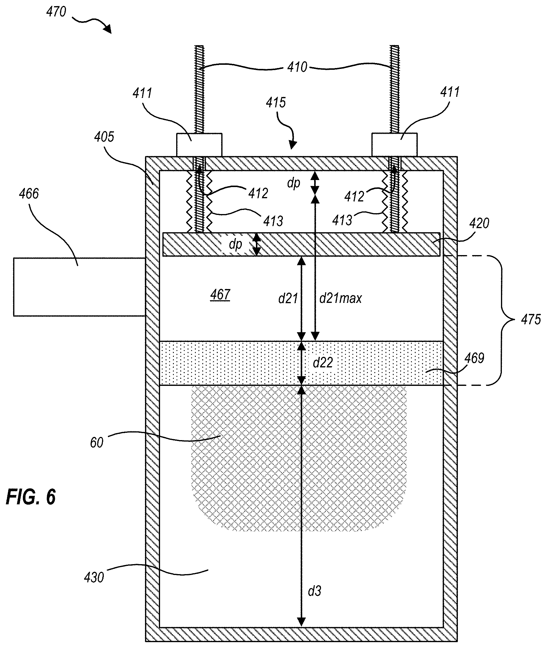
[0013] FIG. 1 schematically illustrates major elements of a plasma processing system, according to an embodiment.
[0014] FIG. 2A is a schematic, isometric view illustrating a portion of a plasma processing system, according to an embodiment.
[0015] FIG. 2B is a schematic top plan view illustrating a conductive plate that forms part of the plasma processing system of FIG. 2A.
[0016] FIG. 3 is a schematic diagram illustrating major components of a system for providing microwaves to a plasma chamber utilizing a waveguide, according to an embodiment.
[0017] FIG. 4 is a schematic cross-sectional drawing illustrating a portion of a plasma processing system that adjusts position of a movable plate within a waveguide cavity, according to an embodiment.
[0018] FIG. 5A is a schematic diagram of a region of FIG. 4, illustrating an RF gasket for reducing microwave leakage between a movable plate and a housing, according to an embodiment.
[0019] FIG. 5B is a schematic diagram of a region of FIG. 4, illustrating a first RF choke for reducing microwave leakage between a movable plate and a housing, according to an embodiment.
[0020] FIG. 5C is a schematic diagram of a region of FIG. 4, illustrating a second RF choke for reducing microwave leakage between a movable plate and a housing, according to an embodiment.
[0021] FIG. 5D is a schematic diagram of a region of FIG. 4, illustrating a third RF choke for reducing microwave leakage between a movable plate and a housing, according to an embodiment.
[0022] FIG. 6 is a schematic cross-sectional drawing illustrating a portion of a plasma processing system that includes most of the features of the plasma processing system of FIG. 4, according to an embodiment.
[0023] FIG. 7 is a schematic cross-sectional drawing illustrating a portion of a plasma processing system that includes most of the features of the plasma processing system of FIG. 6, according to an embodiment.
[0024] FIG. 8 is a schematic cross-sectional drawing illustrating a portion of a plasma processing system that includes most of the features of the plasma processing system of FIG. 7, according to an embodiment.
[0025] FIG. 9 is a schematic cross-sectional drawing illustrating a portion of a plasma processing system that includes similar features as the plasma processing system of FIG. 7, according to an embodiment.
[0026] FIG. 10 is a schematic cross-sectional drawing illustrating a portion of a plasma processing system that includes most of the features and operational concepts of the plasma processing systems of FIG. 4 and FIG. 7, according to an embodiment.
[0027] FIG. 11 is a schematic cross-sectional drawing illustrating a portion of a plasma processing system that includes most of the features and operational concepts of the plasma processing system of FIG. 10, according to an embodiment.
[0028] FIG. 12 is a schematic cross-sectional drawing illustrating a portion of another plasma processing system that includes most of the features and operational concepts of the plasma processing system of FIG. 10, according to an embodiment.
[0029] FIG. 13 illustrates an exemplary pattern of process variation on a workpiece.
[0030] FIG. 14 illustrates the effect of a rotating wave process on the processing of a workpiece, according to an embodiment.
[0031] FIG. 15 illustrates certain radial eigenmodes that can be excited within a chamber having chamber walls, according to an embodiment.
[0032] FIG. 16 illustrates locations of peak electric field strengths corresponding to each of the eigenmodes illustrated in FIG. 15.
[0033] FIG. 17 is a flowchart of a method that generates a plasma for processing a workpiece, according to an embodiment.
[0034] FIG. 18 is a flowchart of a method that provides electromagnetic radiation for powering a plasma in a process chamber, according to an embodiment.
[0035] FIG. 19 is a flowchart of a method for plasma processing in a process chamber, according to an embodiment.
[0036] FIG. 20 is a flowchart of a method 630 for processing a workpiece in a process chamber, according to an embodiment.
[0037] FIG. 21A illustrates workpiece after processing with a nominal plasma process that produces a different result in an outer region than in an inner region, according to an embodiment.
[0038] FIG. 21B schematically illustrates a program that implements a process strategy, where a first process segment proceeds at a nominal power, and thereafter a second process segment continues through an additional time increment, according to an embodiment.
DETAILED DESCRIPTION
[0039] FIG. 1 schematically illustrates major elements of a plasma processing system 100, according to an embodiment. System 100 is depicted as a single wafer, semiconductor wafer processing system, but it will be apparent to one skilled in the art that the techniques and principles herein are applicable to a plasma processing system for any type of workpiece (e.g., items that are not necessarily wafers or semiconductors). Processing system 100 includes an outer housing 110 for a wafer interface 115, a user interface 120, a process chamber 130, a controller 140 and one or more power supplies 150. Process chamber 130 includes one or more pedestals 135, upon which wafer interface 115 can place a workpiece 50 (e.g., a wafer, but could be a different type of workpiece) for processing. Vacuum 160 (e.g., one or more vacuum pumps) are operable to evacuate process chamber 130, and one or more gas supplies 155 can be connected to introduce process gases into process chamber 130. One or more radio frequency or microwave generators (RF Gen) 165 supply power at one or more radio or microwave frequencies to create a plasma within process chamber 130. (The electromagnetic radiation provided by embodiments herein may be called "microwaves" in this disclosure, notwithstanding that the radiation may be within the microwave, radio frequency or other portions of the electromagnetic spectrum.) RF Gen 165 may be external or internal to system 100, and may take the form of one or more electronics sets, described further below. RF Gen 165 transmits microwaves within a waveguide cavity 167 that may be disposed above or below process chamber 130, and is shown in FIGS. 1 and 2A as above chamber 130. Waveguide cavity 167 may be a cylindrical cavity, but this is not strictly required. Process chamber 130 is proximate waveguide cavity 167, and is bounded adjacent to waveguide cavity 167 by at least a plate 169 formed of a dielectric material that is permeable to microwaves, but not to air or process gases utilized in chamber 130. Thus, dielectric plate 169 can support a pressure difference between waveguide cavity 167 and chamber 130 when chamber 130 is evacuated, while allowing microwaves within waveguide cavity 167 to propagate into chamber 130. Dielectric plate 169 may be formed, for example, of refractory material(s) such as silicon dioxide, silicon nitride or intermediate silicon oxynitride compounds; ceramic(s) such as alumina, yttria and the like; plastic(s) and/or polymer(s). In some embodiments, a plurality of hollowed regions is formed on a lower surface of dielectric plate 169. This can help plasma ignition, especially in relatively high pressure (e.g., about 1 Torr or greater) or low power conditions, by helping to disrupt plasma surface modes that can form at the lower surface of dielectric plate 169. Other structures may also exist between waveguide cavity 167 and process chamber 130, as discussed below.
[0040] The elements shown as part of system 100 are listed by way of example and are not exhaustive. Many other possible elements, such as: gas and/or vacuum plumbing, pressure and/or flow controllers; electrodes, magnetic cores and/or other electromagnetic apparatus; mechanical, pressure, temperature, chemical, optical and/or electronic sensors; viewing and/or other access ports; and the like may also be included, but are not shown for clarity of illustration. Internal connections and cooperation of the elements shown within system 100 are also not shown for clarity of illustration. In addition to RF generator 165, other utilities such as gas supplies 155, vacuum 160, and/or general purpose electrical power 170 may connect with system 100. Like the elements shown in system 100, the utilities shown as connected with system 100 are intended as illustrative rather than exhaustive; other types of utilities such as heating or cooling fluids, pressurized air, network capabilities, waste disposal systems and the like may also be connected with system 100, but are not shown for clarity of illustration.
[0041] FIG. 2A is a schematic, isometric view that illustrates a portion of a plasma processing system 200 that includes a waveguide cavity 167, microwave inputs 166 that transmit microwaves into waveguide cavity 167, a process chamber 130, and a workpiece 50 therein. A broken line 2B-2B' indicates a plane of a cross-sectional view illustrated in FIG. 2B. In system 200, a housing 105 defines both waveguide cavity 167 and process chamber 130, and process chamber 130 is substantially radially symmetric about a common axis with waveguide cavity 167. Microwaves propagate from microwave inputs 166 through microwave input openings 162 into waveguide cavity 167, then into process chamber 130 through slots 168 of a conductive plate 137, to provide energy for igniting and/or maintaining a plasma 60. Conductive plate 137 may be formed of metal, for example, but can also be formed of other conductive materials, or conductive materials that are partially or completely coated with protective (and not necessarily conductive) materials. In the embodiment shown in FIGS. 2A and 2B, waveguide cavity 167 is bounded by a dielectric plate 169 that faces, and may be in contact with, conductive plate 137. Dielectric plate 169 may be formed, for example, of refractory material(s) such as silicon dioxide, silicon nitride or intermediate compounds (e.g., silicon oxynitride); ceramic(s) such as alumina, yttria and the like; plastic(s) and/or polymer(s). Conductive plate 137 forms slots 168 that allow microwaves to propagate through dielectric plate 169 and into process chamber 130. Slots 168 may, for example, form a radial line slot antenna. Pedestal 135 is configured to present a workpiece 50 to plasma 60 for processing. Process chamber 130 may include ports and/or mechanical openings (not shown) for insertion and/or withdrawal of workpiece 50, introduction of gases to form plasma 60, removal of plasma and gaseous reaction products, sensors, viewing and the like. Conductive plate 137 may be advantageous in that it may be a good thermal conductor, to help remove heat generated by plasma 60 and by displacement currents within dielectric plate 169. FIG. 2B is a schematic top plan view illustrating conductive plate 137, showing dielectric plate 169 exposed through slots 168.
[0042] The orientation of process chambers, waveguide cavities and the like that is illustrated in FIGS. 2A, 4 and 6-10 is typical, but not required for operation of systems herein. For example, FIG. 2A shows a workpiece 50 that may be a wafer, disposed atop a pedestal 135 that may be a wafer chuck, where gravity could be used to hold the workpiece in place, at least during transfer operations. Thus, in the description below, where the term "height" is used, this should be taken to mean a position or a distance, not necessarily in a vertical direction. Similar terms like "vertical" and "top" do not limit embodiments to the orientations shown, but should be understood as modified according to other orientations in which embodiments may be operated.
[0043] Because the walls and conductive plate 137 of system 200 are equipotential planes, waveguide cavity 167 may support eigenmodes--microwave propagation modes in which, for example, a height d1 of waveguide cavity 167 is a multiple of half axial wavelengths of the microwaves within waveguide cavity 167, such that waveguide cavity 167 is resonant at the corresponding microwave frequency. That is, when d1=m2.pi./k.sub.z, an eigenmode forms at a resonant frequency of waveguide cavity 167. Here, the axial wavenumber k.sub.z is defined as
( .omega. c ) 2 = .kappa. 2 + k z 2 , ##EQU00001##
where .omega. is an angular frequency (.omega.=2.pi.f), f is the frequency of the microwave, m is a positive integer and c is the speed of light, and .kappa. is a radial wavenumber for which a boundary condition on the side-wall of the cavity is satisfied for a radius R of the cavity (i.e., J'.sub.m(y'.sub.mn)=0 and .kappa.=y'.sub.mn/R, where J'.sub.m is a Bessel function of the first kind, of order m, and y'.sub.mn is a Bessel function of the second kind, of order m.)
[0044] For example, in system 200, when a typical microwave frequency of 2.45 GHz is used, one value of d1 will be about 62 mm, but can vary according to shapes and patterns of slots on conductive plate 137, small variations in materials, the exact geometry of microwave input openings 162, and the like. A value of d1 that causes waveguide cavity 167 to support an eigenmode may be designated as an "eigenmode position" herein. Eigenmodes within waveguide cavity 167 advantageously maximize power delivery from the electronics sets into plasma 60, and minimize power that is reflected back to the electronics sets. (A thickness of dielectric plate 169 and a height of process chamber 130 can also be designed to support eigenmode operation of process chamber 130 at the same microwave frequency, as discussed below.)
[0045] It may also be helpful to provide dielectric plate 169 with a thickness and dielectric constant to support a resonance within dielectric plate 169 at the same frequency that supports an eigenmode within waveguide cavity 167. This can be represented as the condition d2=m2.pi./k.sub.dz, where axial wavenumber k.sub.dz is defined as
( .omega. d c ) 2 = .kappa. 2 + k dz 2 , ##EQU00002##
.epsilon..sub.d is the dielectric constant of dielectric plate 169 (or the effective dielectric constant, if dielectric plate 169 is formed of multiple materials), m is any positive integer, and radial wavenumber .kappa. is defined above. The reason that this condition is helpful, is because to ignite plasma 60, it helps to provide high field strength just below dielectric plate 169. Plasma 60 may tend to form and/or be concentrated nearest to dielectric plate 169 within process chamber 130 (where fields coupled through plate 137 are strongest). Additionally, although overall effective height of chamber 130 may not be critical, it can also be chosen to support eigenmode operation of process chamber 130. This condition may be represented as the net "electrical height" being a multiple of the half-wavelength of microwaves to be used, to maximize electromagnetic field strength throughout process chamber 130, that is, d3+d2 {square root over (.epsilon..sub.d)}.apprxeq.m(.lamda./2). And, for the same reasons as noted above with respect to waveguide cavity 167, it may be difficult to ensure the eigenmode condition when conductive plate 137, dielectric plate 169 and process chamber 130 are of fixed construction.
[0046] Dimensional variations, material variations and the like of housing 105, an exact configuration of slots 168 within conductive plate 137, distribution of plasma 60 under dielectric plate 169, and/or asymmetric features such as sensors, fasteners, access ports and the like associated with waveguide cavity 167 can shift an effective value of an eigenmode position, either globally or from place to place within waveguide cavity 167. Therefore, while housing 105 and conductive plate 137 may be fabricated with an intent that d1 defines an eigenmode position, an actual value d1 may not be an eigenmode position, as intended. Apparatus and methods for adjusting d1 and other dimensions of cavities and chambers herein are disclosed below in connection with FIGS. 4-6 and FIGS. 10-12.
[0047] An optimal thickness of dielectric plate 169 may also be governed by other requirements such as cost, size, weight, mechanical strength and ability to maintain a vacuum seal over process chamber 130. Process chamber 130 may be sized to accommodate workpieces 50 that are up to 300 mm or 450 mm in diameter (e.g., wafers of about 12 inches or about 18 inches nominal diameter). Therefore, dielectric plate 169 may be required to support a vacuum pressure differential across an area of about 0.15 m.sup.2 to 0.25 m.sup.2, exerting a net force of about 22 to 40 pounds at normal atmospheric pressure. When dielectric plate 169 is formed of a refractory material with a dielectric constant of about 4 or a ceramic with a dielectric constant of about 10, thicknesses less than about 10 mm may be too fragile, while thicknesses greater than about 80 mm may be too costly, large and heavy. Within this exemplary range, exact thicknesses to be used can be optimized according to the wavelength of the microwave radiation to be used and the actual dielectric constant of the material to be used, as discussed above.
[0048] FIG. 3 is a schematic diagram illustrating major components of a system 300 for providing microwaves to a plasma chamber utilizing a waveguide. A waveguide 210 of system 300 may be for example waveguide cavity 167, FIGS. 1 and 2A. In general, system 300 powers waveguide 210 at two locations noted as P and Q in FIG. 3. Locations P and Q are typically driven at a common frequency (by electronics sets 225(1), 225(2), described below) with a phase offset that may correspond to the angular offset between P and Q around a circumference of waveguide 210. A coordinate reference system is shown within waveguide 210. An axial direction z denotes distance along a cylindrical axis that is concentric with waveguide 210; that is, direction z is in and out of the plane of FIG. 3. A radial direction r denotes distance from the cylindrical axis. An azimuthal direction .theta. denotes angular position about the cylindrical axis. Location P is taken as the origin of the .theta. direction, as shown.
[0049] Waveguide 210 is thus considered a dual driven waveguide; the dual driven mode of operation provides high microwave energy density derived from two sets of driving electronics rather than a single set operating at double the power. Use of two (or more) sets of driving electronics, each operating at lower power than a single set at high power, may be advantageous. An electronics set operating at higher power may require components having higher voltage, current, or heat dissipation ratings that may be much more expensive or difficult to obtain than components for lower power sets. For example, microwave field effect transistors (FETs) of low cost and high quality have recently become available for use in electronics sets 225 herein, but high voltage, current, and/or power dissipation versions of such FETs may remain costly or difficult to obtain.
[0050] Operation of system 300 is best understood as starting with a signal generator 215 that provides two microwave signals 220(1), 220(2) that are at the same frequency, but may have a phase offset with respect to one another, that may correspond to a mechanical offset between the driving locations. For example, if locations P and Q are located 90 degrees away from one another about a circumference of waveguide 210, the nominal phase offset would be .pi./2. Determining and controlling corrections to phase offset is discussed immediately below. In certain embodiments, signal generator 215 may control frequency and/or amplitude of signals 320, as well as phase thereof. An application of controlling frequency is to tune system 300 so that eigenmode conditions can be established in waveguide 210 and an adjacent process chamber. This can be done to correct electronically for difficult-to-control irregularities in waveguide and chamber dimensions, materials, asymmetric chamber features and the like, although mechanical approaches can also be taken (e.g., see FIGS. 4-6 and FIGS. 10-12 below). An application of controlling amplitude is to provide rotating mode control such that local irregularities in the generated plasma can be smoothed out, as discussed further below (e.g., see FIGS. 13, 14).
[0051] Microwave signals 220(1), 220(2) drive circuits that are referred to as a first electronics set 225(1) and a second electronics set 225(2). Each electronics set 225(1), 225(2) begins with a solid state amplifier 230 that boosts the power of respective microwave signals 220(1), 220(2) to create amplified microwave signals 235(1), 235(2). Solid state amplifiers 230 may include one or more microwave FETs, as discussed above. Each amplified microwave signal 235(1), 235(2) passes into and through a circulator 240 that serves to protect the respective solid state amplifiers 230 from power reflections from waveguide 210. Circulators 240 thus pass input power from solid state amplifiers 230 into respective tuners 250, while shunting any power that is reflected back into dummy loads 245.
[0052] Tuners 250 adjust impedance seen by the amplified microwave signals 235(1), 235(2) so as to match an impedance presented by components such as coaxial-to-waveguide converters 265, waveguide 210 and an adjacent process chamber (e.g., process chamber 130, FIG. 1, not shown in FIG. 3). Tuners 250 may be, for example, three-pole stub tuners. The amplified, tuned signals then pass through respective coaxial-to-waveguide converters 265 and into waveguide 210 at respective waveguides with radiating apertures 270 (corresponding to the schematically designated microwave inputs 166 ending in microwave input openings 162, FIG. 2A).
[0053] As part of the tuning required to achieve acceptable impedance matching, tuners 250 can change the phase of signals passed toward waveguide 210, such that although the signals are supplied at positions that have a mechanical phase offset around the circumference of waveguide 210, the signals themselves may no longer have the same electrical phase offset. For example, if P and Q are mechanically offset by 90 degrees, the tuners may shift the phase offset between microwaves at P and Q to a value other than .pi./2. Thus, instead of exciting a symmetric, circularly rotating mode in waveguide 210, an asymmetric, ellipsoidally or linearly rotating mode may be excited. This asymmetry in the microwave configuration can lead, in turn, to process aberrations in an adjacent process chamber (e.g., process chamber 130, FIGS. 1, 2A, where a plasma is powered by the microwaves in waveguide 210). For example, an asymmetric microwave configuration can lead to a correspondingly asymmetric plasma and consequently to local skews in depth of plasma etching.
[0054] One approach to addressing the type of asymmetry noted above is to provide electrical correction to the phase delay between microwave signals 220(1) and 220(2), and thus between amplified microwave signals 235(1) and 235(2). For example, dual phase signal generator 215 may receive a correction signal 313 from a signal controller 312 that provides information for adjustment of signals 220(1), 220(2). For example, correction signal 313 may direct dual phase signal generator 215 to provide a corrected or targeted phase offset between microwave signals 220(1), 220(2). Thus, in system 300 with a mechanical offset of .pi./2 between points P and Q, microwave signals 220(1), 220(2) may be out of phase with one another by .pi./2, or by .pi./2 plus or minus a target phase difference, such that a measured phase difference at points P and Q is as intended, as discussed below. In another example, correction signal 313 may direct dual phase signal generator 215 to boost and/or attenuate one or both of microwave signals 320(1), 320(2), which may advantageously help preserve a circular rotation of the microwave field.
[0055] Monitoring antennas 211(1) and 211(2) may be disposed at locations that are 180 degrees across waveguide 210 from points P and Q respectively, and provide analog signals to signal controller 312 through their respective connections 318(1) and 318(2). These measurements, within waveguide 210 itself, will capture any phase and/or amplitude offset introduced by tuners 250. Monitoring antennas 211 may monitor either an electrical field or a magnetic field component of microwaves in waveguide 210. The locations of monitoring antennas 211(1) and 211(2) 180 degrees across waveguide 210 from points P and Q (or at least each antenna 211 being at least 30 degrees away from either of P and Q) may enable the signals returned to signal controller 312 to include effects of waveguide 210 that are not readily monitored by monitoring antennas located at points P and Q. Signal controller 312 may receive signals from monitoring antennas 211(1) and 211(2) through their respective connections 318(1) and 318(2) and may determine amplitude of, and a phase offset between, signals at points P and Q. For example, signal controller 312 may perform in-phase and quadrature-phase demodulation (IQ demodulation) to measure amplitude and phase offset of the signals from monitoring antennas 211(1) and 211(2). Signal controller 312 may then utilize measured phase offset and/or amplitudes to calculate and provide a corresponding digital correction signal 313 to dual phase signal generator 215. Digital correction signal 313 may be chosen to be a desired phase offset (e.g., a value of .pi./2) or an offset from an assumed, desired phase difference (e.g., a correction factor that is zero when the desired phase difference is attained). Alternatively, digital correction signal may be chosen to adjust amplitude of one or both of microwave signals 320(1), 320(2). Dual phase signal generator 315 may then provide microwave signals 320(1) and 320(2) with a phase offset and/or amplitudes such that when the microwave signals propagate through the system, the phase offset between points P and Q is driven to the desired phase difference, and/or the amplitudes measured at points P and Q are as desired.
[0056] Optionally, a user input device 314 may provide one or more target parameters 316 to signal controller 312. User input device 314 may be implemented in a variety of ways, such as by physical switches providing an output that is received directly by signal controller 312, or as a part of system management hardware and software that acquires the target parameters from a user interface (e.g., a keyboard, other buttons, or a graphical user interface (GUI)). Target parameters 316 may include, for example, a desired phase difference as measured at monitoring antennas 211(1) and 211(2), or amplitude adjustments to either or both of microwaves driven into waveguide 210. Target parameters 316 can be utilized by signal controller 312 along with the analog signals from monitoring antennas 211(1) and 211(2), to generate digital correction signal 313. For example, when a target phase difference is utilized, digital correction signal 313 may be generated first based on the signals from monitoring antennas 211(1) and 312(1), after which digital correction signal 313 may be adjusted by adding or subtracting target parameter 316. Once digital correction signal 313 is transmitted, dual phase signal generator 315 may provide signals 320(1) and 320(2) with a corresponding offset until the phase offset between points P and Q is driven according to the target parameter, and digital correction signal 313 is driven to its target value, or zero. In another example, when a target amplitude adjustment is utilized, dual phase signal generator 215 can adjust amplitude of either or both of signals 320(1), 320(2) in response thereto.
[0057] Optional user input device 314 may thus provide a useful, independent degree of freedom for optimizing a semiconductor processing system that includes system 300 or other systems with a similar capability, as disclosed herein. For example, a corresponding semiconductor processing system may be optimized by processing (e.g., etching) wafers. Each wafer could be processed with identical processing parameters except for a different target parameter entered into user input device 314. The performance of the system could be evaluated by measurements of the wafers that are indicative of performance of the etch system (e.g., etch rate, selectivity, linewidth change due to etch, and the like) as well as system monitors (e.g., system stabilization times, endpoint detection parameters, etc.) An optimized value of the target parameter could then be selected, based on the wafer measurements, the system monitors and/or a combination thereof.
[0058] It will be understood by one skilled in the art that while signal controller 312 cooperates with dual phase signal generator 215 to adjust phase of microwave signals 320(1) and 320(2), tuners 250 also continue to adjust impedance matching to minimize reflected power. Thus, system 300 does not sacrifice impedance matching, but rather provides the additional capability of phase and/or amplitude adjustment for electronics sets 255(1) and 255(2), to optimize plasma symmetry in a process chamber adjacent to waveguide 210. That is, in embodiments, signal generator 315 adjusts the phase offset, and tuners 250 provide the impedance matching, concurrently with one another during the operation of system 300. In other embodiments, signal generator 315 adjusts the amplitude, and tuners 250 provide the impedance matching, concurrently with one another during the operation of system 300.
[0059] Embodiments herein recognize that as wafer sizes grow larger and the geometries produced in semiconductor fabrication grow smaller, the need for uniformity control of all aspects of the processing environment around the wafer increases. Therefore, embodiments herein adjust the microwave configuration that generates the plasma, not only to match impedance, but also to adjust phase and/or amplitude after impedance is matched, for improved symmetry of the plasma generated around the wafer. Even when careful attention is paid to symmetry of a process chamber, placement of a wafer in the process chamber, and the like, asymmetries in a plasma can arise from many causes (e.g., mechanically asymmetric ports for gas or plasma input and outlets, sensors, wafer placement, wafer flats, cabling length, material variations in any of the above components, and the like). To correct for these causes, additional degrees of control, in addition to impedance matching, may provide extra and useful tools for improving uniformity in plasma processing. While system 300 provides some control through electronic adjustments of amplitude and phase, further mechanical and electrical adjustments described below are also useful.
[0060] FIG. 4 is a schematic cross-sectional drawing illustrating a portion of a plasma processing system 400 that adjusts a height d1 of a movable conductive plate 420 within a waveguide cavity 467. In system 400, a conductive plate 437 that is coupled with housing 405 forms a lower bound of a waveguide cavity 467. A dielectric plate 469 is adjacent to, and in direct contact with, conductive plate 437. Similar to the discussion above in connection with FIG. 2A, d1 and d2 affect the ability of waveguide cavity 467 and dielectric plate 469, respectively, to support eigenmodes. While frequency adjustment can be used to adjust one or the other of these arrangements to support an eigenmode, the frequency adjustment may not create eigenmode conditions simultaneously in both waveguide 467 and dielectric plate 469. That is, an additional degree of freedom in adjustments may be useful.
[0061] System 400 includes one or more adjustment devices 410 that couple with housing 405 and movable conductive plate 420. Movable conductive plate 420 faces process chamber 430 across microwave cavity 467, that is, plate 420 is on a distal side of waveguide cavity 467 from the process chamber 430. Adjustment devices 410 are shown as threaded rods in FIG. 4, but as discussed below, many other types of adjustment devices may be used. In the embodiment illustrated in FIG. 4, devices 410 extend through openings 412 in a ceiling plate 415 of a housing 405. A height of each device 410, and a corresponding height of movable conductive plate 420 within housing 405, can be adjusted with a corresponding nut 411. This additional degree of freedom allows, for example, a microwave frequency to be tuned first, to support the eigenmode condition within plate 469; then, d1 can be tuned so that movable conductive plate 420 is at an eigenmode position within waveguide 467. By tuning each of these structures to support their respective eigenmodes, efficient coupling and high field strength at a lower surface of dielectric plate 469 (e.g., for igniting a plasma) is provided. d3 represents a height of dielectric plate 469 over a floor surface of process chamber 430, and will be constrained at least somewhat by the need to provide clearance for a workpiece holder and a workpiece itself (e.g., pedestal 135 and workpiece 50, FIG. 2A).
[0062] Like conductive plate 137 discussed above, conductive plates 437 and 420 may be formed of metal, for example, but can also be formed of other conductive materials, or conductive materials that are partially or completely coated with protective (e.g., not necessarily conductive) materials.
[0063] Although adjustment devices of rods and nuts are shown to illustrate the concept of adjustment devices 410, it will be clear to one skilled in the art that any type of mechanical or electromagnetic actuator may be substituted for the rod and nut combination shown. For example, geared devices, spring loaded devices, magnetic actuators, stepper motors, piezoelectric actuators or other electromagnetic devices could be substituted. One of ordinary skill in the art, upon reading and comprehending the present disclosure, will readily recognize alternatives, equivalents, modifications, and intermediate combinations that can be used as adjustment devices or actuators. In some embodiments, a plurality of hollowed regions is formed on a lower surface of dielectric plate 469 to promote plasma ignition, as discussed in connection with dielectric plate 169, FIG. 1.
[0064] Certain embodiments utilize a single device 410 to adjust d1 across waveguide cavity 467, while other embodiments use three devices 410 to adjust a plane formed by movable conductive plate 420 with respect to plate 437. Connections of devices 410 to movable conductive plate 420 may include flexible materials or joints that allow movable conductive plate 420 to tilt with respect to devices 410. Still other embodiments may use more devices 410 with a deformable conductive plate 420, to provide point to point control over d1 and microwaves in waveguide cavity 467 without regard to planarity of movable conductive plate 420 or underlying plate 437. Optionally, each device 410 is surrounded above movable conductive plate 420 by a conductive bellows 413 that couples mechanically and electrically with ceiling plate 415. Bellows 413 thus ensures that movable conductive plate 420 is at the same electrical potential as housing 405, and can contain any particles that may be shed where devices 410 pass through ceiling plate 415 and engage nuts 411.
[0065] In system 400, a small gap may be needed between movable conductive plate 420 and sides of housing 405, to ensure that conductive plate 420 can move freely. This can adversely affect the propagation of microwaves within waveguide cavity 467 by allowing propagation of some microwaves through the gap, which can disturb the eigenmode condition. A region denoted as A in FIG. 4 is illustrated in FIGS. 5A through 5D, with options for managing this effect. The RF gasket illustrated in FIG. 5A, or one of the RF chokes illustrated in FIG. 5B, may be installed about movable conductive plate 420, and will thus be present in region A' as well as region A (e.g., A and A' are 180 degrees about a circumference of housing 405 from one another).
[0066] FIG. 5A illustrates an RF gasket 440 inserted between movable conductive plate 420 and housing 405. RF gasket 440 will generally reduce microwave leakage effectively, but may scrape against either or both of movable conductive plate 420 and housing 405. This may generate metal particles, which may undesirably affect and move around waveguide cavity 467 in response to microwaves.
[0067] FIG. 5B illustrates an RF choke 431 including a conductive holder 442 that is coupled with movable conductive plate 420, and a dielectric material 444 held by holder 442 against a top surface of movable conductive plate 420. Advantageously, dielectric material 444 has a lateral dimension
L 1 = m .lamda. 2 1 , ##EQU00003##
where .epsilon..sub.1 is a dielectric constant of material 444, .lamda. is the wavelength of the microwaves and m is any integer greater than zero.
[0068] FIG. 5C illustrates an RF choke 432 including the features of RF choke 431, and adds a second dielectric material 445. Advantageously, dielectric material 444 has a dimension
L 2 = p .lamda. 2 2 , ##EQU00004##
where .epsilon..sub.2 is the dielectric constant of material 445, .lamda. is the wavelength of the microwaves and p is any integer greater than zero. Consideration should be given to the fact that the dielectric will rub against housing 405; soft and/or non-shedding dielectrics such as polytetrafluoroethylene (e.g., Teflon.RTM.) or polyetheretherketone (PEEK) may be useful as material 445.
[0069] FIG. 5D illustrates an RF choke 433 including only second dielectric material 445. In this embodiment, dielectric material 445 advantageously has a dimension
L 3 = n .lamda. 2 2 , ##EQU00005##
where .epsilon..sub.2 is the dielectric constant of material 445, .lamda. is the wavelength of the microwaves and n is any odd integer greater than zero. L3 is chosen so as to prevent the excitation of electromagnetic waves in the dielectric filled gap, thus reducing microwave leakage through the gap.
[0070] Certain embodiments herein can address situations such as when the signal generator, amplifying electronics and/or other components (e.g., electronics sets 225, FIG. 3) cannot provide a broad enough tuning range, or a large variety of resonant modes are desired. One approach to this is to remove the conductive plate bounding the waveguide cavity (e.g., cavities 167 or 467) such that the housing (e.g., housing 405) defines a single cavity.
[0071] FIG. 6 is a schematic cross-sectional drawing illustrating a portion of a plasma processing system 470 including most of the features of plasma processing system 400, FIG. 4. However, system 470 does not include a conductive plate at the bottom of cavity 467. Because the components that are used in system 470 are the same as those in system 400, the same reference numerals are used for such components, but because the electrical behavior is different, some of the dimensions are noted differently. d21 now represents an air gap height of cavity 467, while d22 represents a thickness of dielectric plate 469.
[0072] Electrically, system 470 is a single cavity bounded by housing 405 and movable conductive plate 420 having a thickness dp. However, thickness and dielectric constant of dielectric plate 469, as well as dimension d21 shown, will still have effects on how microwaves propagate within the cavity, including effects on eigenmode conditions. Thus, a mechanism for adjusting height of movable conductive plate 420, here shown again as adjustment devices 410 and nuts 411, remains a useful tool for tuning microwave conditions within cavity 467. Of course, it is clear to one skilled in the art that any type of mechanical or electromagnetic actuator may be substituted for the rod and nut combination shown; all of the discussion about these features in connection with system 400 is equally applicable to system 470. With such height adjustment device in place, d21 can be thought of as a variable with a minimum value of zero to a maximum value of d21max, where movable conductive plate 420 will abut ceiling plate 415 (a lower surface of movable conductive plate 420 will be the thickness of the movable plate, dp, below ceiling plate 415). In practice the limits of zero and d21max may be further limited by travel limits of the movable plate mechanism.
[0073] System 470 is advantageously adjustable to support at least one eigenmode within a portion of housing 405 designated as cavity 475. This allows fields to be efficiently coupled down to a lower surface of dielectric plate 469, where they will couple into plasma 60. When d21 is at its minimum value, the eigenmode will have a maximum frequency of f.sub.max; when d21 is at its maximum value, the eigenmode will have a minimum frequency of f.sub.min. Advantageously, electronics sets driving microwave inputs 466 support all frequencies from f.sub.min to f.sub.max so that an eigenmode can be supported for any physical setting of movable conductive plate 420. There will typically be one eigenmode position available for movable conductive plate 420, for any frequency available from the electronics sets, although if d21max is sufficiently large, there may be more than one eigenmode position available.
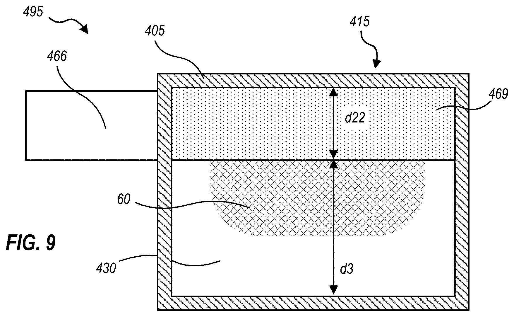
[0074] FIG. 7 is a schematic cross-sectional drawing illustrating a portion of a plasma processing system 480 including most of the features of plasma processing system 470, FIG. 6. However, system 480 does not include a movable ceiling plate. When characteristics of housing 405, components therein, and dimensions d21 and d22 are well known and/or controlled, it becomes possible to provide a unitary housing with vacuum sealed dielectric plate 469 therein, with the dimensions tuned such that an eigenmode is supported by cavity 485, analogous to cavity 475 of system 470, FIG. 6. Furthermore, if electronics sets driving microwave inputs 466 support frequency adjustment, it may be possible to tune frequency of the microwaves to support an eigenmode within cavity 485, notwithstanding the fact that d21 and d22 are fixed. Alternatively, if d21 can be adjusted before housing 405 is sealed (e.g., by characterizing system 480 under power, with a temporary mechanism for adjusting height of dielectric plate 469, that can later be withdrawn) then a finished system 480 can be provided in a more compact form with fewer active parts or adjustments. Similarly to system 400, FIG. 4, considerations of size, weight, cost, materials to be used, and the like can be used to select dimensions d21 and d22. d22, in particular, needs to be thick enough to withstand the force of atmospheric pressure across dielectric plate 469 when process chamber 430 is evacuated, but when d22 is very high, dielectric plate 469 may become heavy and costly.
[0075] FIG. 8 is a schematic cross-sectional drawing illustrating a portion of a plasma processing system 490 including most of the features of plasma processing system 480, FIG. 7. However, system 490 is powered from a top-injecting microwave input 468, instead of side-injecting microwave input 466 shown in systems 400, 470 and 480, FIGS. 4, 6 and 7. Although other embodiments could theoretically use top-injecting microwave inputs like input 468, integrating such inputs with the movable plates of such embodiments may be difficult. Like system 480, system 490 can be provided in a compact form, especially in applications where integrating one or more side-injecting microwave inputs 466 is problematic.
[0076] The design of FIGS. 7 and 8 can be further modified, in embodiments, by reducing d21 to zero. FIG. 9 is a schematic cross-sectional drawing illustrating a portion of a plasma processing system 495 that includes similar features as plasma processing system 480, FIG. 7, with d21 set to zero, that is, eliminating cavity 467. Like systems 480 and 490, system 495 can be provided in a compact form. In alternate embodiments of system 495, the side-injecting microwave input 466 can be replaced with top-injecting microwave input 468 of system 490, FIG. 8.
[0077] FIG. 10 is a schematic cross-sectional drawing illustrating a portion of a plasma processing system 500 including most of the features and operational concepts of plasma processing system 400, FIG. 4, and processing system 480, FIG. 7. System 500 introduces a gap 510 between plate 437 and a dielectric plate 520 that, similar to dielectric plate 469, seals off process chamber 430 from gap 510 and cavity 467 such that those regions are not evacuated when process chamber 430 is evacuated. A cavity 505 can be defined to include gap 510 and dielectric plate 520. Then, in similar manner to processing system 480, FIG. 7, if electronics sets driving microwave inputs 466 support frequency adjustment, it may be possible to tune frequency of the microwaves to support an eigenmode within cavity 505, notwithstanding the fact that d21 and d22 are fixed. That is, the frequency adjustment can be used to tune cavity 505 to support another one eigenmode, while movable conductive plate 420 can be used to tune cavity 467 to support another, possibly similar eigenmode (e.g., if TE.sub.112 is excited within cavity 505, TE.sub.111 may advantageously be excited within cavity 467).
[0078] FIG. 11 is a schematic cross-sectional drawing illustrating a portion of a plasma processing system 550 including most of the features and operational concepts of plasma processing system 500, FIG. 10. System 550 introduces an adjustable dielectric layer 530 of controllable height, which may be, for example, a layer of a liquid dielectric (or a bladder filled with the liquid dielectric) that does not absorb significant energy at microwave frequencies. A suitable material for adjustable dielectric layer 530 is perfluoropolyether (PFPE), which has a dielectric constant of .epsilon.=1.94 and a loss tangent of tan .delta.=2.times.10.sup.-4. A cavity 505 can be defined as including gap 510, adjustable dielectric layer 530 and dielectric plate 520. Height d21 within cavity 505 can be defined as an electrical length sum of a height d211 of gap 510 and a height d212 of adjustable dielectric layer 530, i.e. d21=d211+ {square root over (.epsilon..sub.liquid)} d212, where .epsilon..sub.liquid is the dielectric constant of dielectric layer 530. A controller 540 can add or remove portions of the liquid dielectric through a fluid connection, and thus mechanically regulate adjustable dielectric layer 530 to create or maintain an eigenmode condition within cavity 505. This provides an extra degree of freedom for optimizing operation of system 550, in that movable conductive plate 420 can be used to optimize cavity 467 and adjustable dielectric layer 530 can be used to optimize cavity 505, without needing to tune a frequency of microwaves supplied through microwave input 466. Thus, if electronics sets powering microwave input 466 are tunable, the tunability can be reserved for optimizing other features (e.g., creating or maintaining an eigenmode condition within process chamber 430). Alternatively, non-tunable electronics sets can be used, to reduce cost.
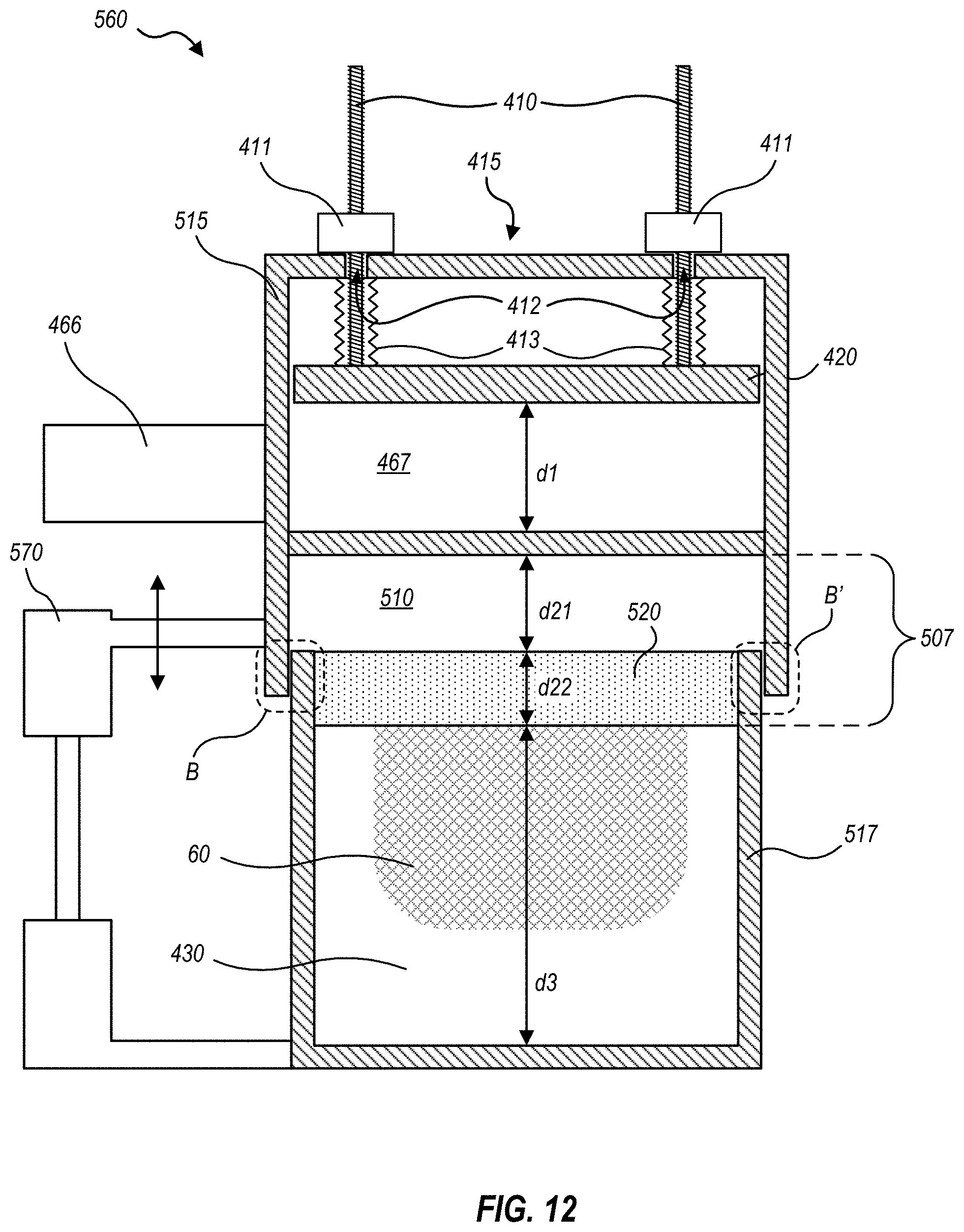
[0079] FIG. 12 is a schematic cross-sectional drawing illustrating a portion of a plasma processing system 560 including most of the features and operational concepts of plasma processing system 500, FIG. 10. System 560 introduces an upper housing 515 that includes microwave cavity 467, and a lower housing 517 that includes process chamber 430. Relative positions of upper housing 515 and lower housing 517 are adjusted through an actuator 570 that, like adjustment devices 410, may be mechanical, magnetic, electromagnetic, piezoelectric or the like. Adjusting the relative positions of upper housing 515 and lower housing 517 causes a height of gap 510 to increase or decrease, respectively. A cavity 507 can be defined as including gap 510 and dielectric plate 520, thus, extension or contraction of actuator 570 can be used to tune cavity 507 in a similar manner as adjustable dielectric layer 530 tunes cavity 505 of system 550 (FIG. 11). The RF gasket illustrated in FIG. 5A, or one of the RF chokes illustrated in FIG. 5B, may be installed at the interface between upper housing 515 and lower housing 517, and will thus be present in region B' as well as region B (e.g., B and B' are 180 degrees about a circumference of housings 515, 517 from one another).
[0080] Methods now discussed provide a means of mitigating local effects of nonuniformities during processing. Dimensional variations, material nonuniformities, apparatus asymmetries and the like can cause certain regions of a process chamber to have more intense plasma action than other areas. These effects may be localized or generalized within a system; that is, some process nonuniformities may affect individual locations that are difficult to predict in advance, while other nonuniformities may be predictably radial or azimuthal relative to the cylindrical form of waveguide 210. When these effects occur, corresponding areas of a workpiece 50 processed by the plasma may be processed nonuniformly.
[0081] FIG. 13 illustrates an exemplary pattern of process variation on a workpiece 50 (e.g., a semiconductor wafer). A region 580 is processed with nominal results, while a region 588 is processed with a degraded result due to one or more small variations in parameters such as gas distribution uniformity, electric field uniformity, variation in process chamber materials, and/or existence of asymmetrical items such as sensors, access ports, workpiece handling equipment and the like associated with the process chamber. A significant difference in appearance between regions 580 and 588 is for purposes of illustration only. That is, region 588 may receive processing (e.g., etching or deposition) that may only be a few percent different from that received in region 580, but it would still be desirable to reduce that percentage as much as possible.
[0082] In embodiments, the effects of region 588 may be made to rotate about workpiece 50 through purely electrical means, while workpiece 50 itself remains stationary. FIG. 14 illustrates the effect of a slow rotating wave process on the processing of workpiece 50. The terms "slow rotating" or "slowly rotating" are used herein to mean wave patterns that change over time at a rate or frequency much lower (e.g., not more than 1/1000.sup.th) than the propagation frequency of electromagnetic radiation. For example, nominal microwave frequencies herein may be about 2.5 GHz, but slow rotating modes will have frequencies <1 MHz, and often <10 KHz.
[0083] A ghost outline of region 588, designated as 588', can be made to rotate over workpiece 50 in an anticlockwise direction, as shown (and could similarly rotate in a clockwise direction). Rotating region 588' may be seen as smoothing or smearing out the effects originally present in region 588, so that no part of workpiece 50 is affected to the same extent as the original region 588. In the example shown, region 588' does not happen to rotate over inner and outer regions of workpiece 50, so these regions remain designated as regions 580'. A small portion of region 588' rotates over bands 582 near the inner and outer regions of workpiece, while a large portion of region 588' rotates over a band 584 between bands 582. (It should be understood that workpiece 50 is depicted with bands for illustrative purposes only; the processing effects will fade into one another gradually, instead of making step function changes at edges of bands 582 and/or 584.) Accordingly, the process effects present in original region 588 can be spread over larger areas and will be reduced across bands 582 and 584, as compared to the concentration of such process effects in original region 588.
[0084] Choosing .OMEGA. such that many field rotations occur during the course of a plasma process allows a corresponding plasma nonuniformity to be rotated, thus smoothing out the effect of "hot" or "cold" processing spots (e.g., like region 588) that are caused by the nonuniformity, on a workpiece. .OMEGA. may also be adjusted empirically by the user, according to measured process uniformity results.
[0085] The effects of a rotating wave pattern within a waveguide cavity on a plasma generated in an adjacent process chamber can also be different, depending on the speed of the rotation. When .OMEGA. is under about 100 Hz, plasma ignition can follow the field rotation closely. Consequently, not only the fields but also the plasma, rotate at the rotational frequency .OMEGA.. When .OMEGA. is over about 1000 Hz, the plasma cannot follow the field, yet is sensitive to the overall distribution of electrical field strength, producing a radially symmetric, uniform plasma distribution. At intermediate values between about 100 Hz and 1000 Hz, the effect is a blend of the rotating and radially symmetric plasma distributions. There can also be interactions between localized plasma effects due to random causes, and rotational frequency, such that sometimes adjusting rotational frequency .OMEGA. increases or decreases local processing nonuniformities. These interactions can be located by characterizing process performance over a variety of rotational frequencies .OMEGA., and choosing a value of .OMEGA. that provides the best uniformity. Advantageously, these effects can be implemented purely electronically, for example by having a user simply input a desired value of and having a controller of the process equipment (e.g., signal generator 215) calculate the appropriate microwave signals as per the following discussion. That is, no mechanical equipment modification is necessary.
[0086] Now consider the configurations of any of the above-mentioned systems 200, 300, 400, 470, 480, 495, 500, 550 and 560, in the context of the coordinate system shown with system 300, FIG. 3. In some of the embodiments discussed, slow wave rotation with a rotational angular frequency
.OMEGA. ( .OMEGA. 2 .pi. ~ 0.1 - 1000 Hz ) ##EQU00006##
for the generalized TE and TM mode (e.g., TE.sub.mnl/TM.sub.mnl) is provided as a means of mitigating local effects of nonuniformities during processing.
[0087] Assume microwaves are injected at a carrier frequency .omega. from microwave inputs P and Q in system 300, FIG. 3, with a time-variable amplitude proportional to cos(.OMEGA.t), and cos(.OMEGA.t+.phi.), respectively. Here .phi. denotes a temporal phase delay to be determined later, and t denotes time. The TE.sub.mnl/TM.sub.mnl mode in the cylindrical cavity excited by the injection from microwave input P can be represented as:
A.sub.p=a cos .OMEGA.t[cos(.omega.t-m.theta.)+cos(.omega.t+m.theta.)] Eq. (1)
where terms depending on the radial (r) and axial (z) coordinates are included in coefficient a, and m is a positive integer.
[0088] Eq. (1) may also be written in the complex form:
A p = a 2 e j .OMEGA. t { e j ( .omega. t - m .theta. ) + e j ( .omega. t + m .theta. ) + e - j ( .omega. t - m .theta. ) + e - j ( .omega. t + m .theta. ) } Eq . ( 2 ) ##EQU00007##
[0089] In the same manner, the TE.sub.mnl/TM.sub.mnl mode excited by the injection from microwave input Q can be described in the complex form as:
A q = a 2 e j .OMEGA. t e j .PHI. { e j ( .omega. t - m ( .theta. - .theta. q ) ) + e j ( .omega. t + m ( .theta. - .theta. q ) ) + e - j ( .omega. t - m ( .theta. - .theta. q ) ) + e - j ( .omega. t + m ( .theta. - .theta. q ) ) Eq . ( 3 ) ##EQU00008##
[0090] Rewriting Eqs. (2) and (3),
A p = a 2 e j .OMEGA. t [ e j .omega. t { e - jm .theta. + e jm .theta. } + e - j .omega. t { e jm .theta. + e - jm .theta. } ] = 2 ae j .OMEGA. t cos ( m .theta. ) cos ( .omega. t ) Eq . ( 4 ) A q = a 2 e j .OMEGA. t [ e j .omega. t { e - jm .theta. e j ( m .theta. q + .PHI. ) + e jm .theta. e j ( - m .theta. q + .PHI. ) } + e - j .omega. t { e jm .theta. e j ( - m .theta. q + .PHI. ) + e - jm .theta. e j ( m .theta. q + .PHI. ) } ] Eq . ( 5 ) ##EQU00009##
[0091] Hence, the resulting wave in the cavity is given by
A s = A p + A q = a 2 e j .OMEGA. t { e j .omega. t [ e - jm .theta. { 1 + e j ( m .theta. q + .PHI. ) } + e jm .theta. { 1 + e j ( - m .theta. q + .PHI. ) } ] + e - j .omega. t [ e jm .theta. { 1 + e j ( - m .theta. q + .PHI. ) } + e - jm .theta. { 1 + e j ( m .theta. q + .PHI. ) } ] } Eq . ( 6 ) ##EQU00010##
[0092] To provide an anti-clockwise rotation, the following condition must be satisfied:
e.sup.j(m.theta..sup.q.sup.+.phi.)=1 Eq. (7)
e.sup.j(-m.theta.sq.sup.+.phi.)=-1 Eq. (8)
[0093] Or, equivalently,
m.theta..sub.q+.phi.=2r.pi. Eq. (9)
-m.theta..sub.q+.phi.=(2s+1).pi. Eq. (10)
[0094] where r and s are arbitrary integers.
[0095] Solving Eqs. (9) and (10) simultaneously, the condition for the anti-clockwise rotation can be represented as
.PHI. ant = 2 r + 2 s + 1 2 .pi. Eq . ( 11 ) .theta. q = 2 r - ( 2 s + 1 ) 2 m .pi. Eq . ( 12 ) ##EQU00011##
[0096] In the same manner, for a clockwise rotation, Eqs. (7) and (8) become
e.sup.j(m.theta..sup.q.sup.+.phi.)=-1 Eq. (13)
e.sup.j(-m.theta..sup.q.sup.+.phi.)=1 Eq. (14)
[0097] and Eqs. (9) and (10) become
m.theta..sub.q+.phi.=(2r+1).pi. Eq. (15)
-m.theta..sub.q+.phi.=(2s+2).pi. Eq. (16)
[0098] Solving Eqs. (15) and (16) simultaneously, the condition for the clockwise rotation can be represented as
.PHI. clk = 2 r + 2 s + 1 2 .pi. + .pi. Eq . ( 17 ) .theta. q = 2 r - ( 2 s + 1 ) 2 m .pi. Eq . ( 18 ) ##EQU00012##
[0099] Comparing Eqs. (11) & (12) with (17) & (18), the angle .theta..sub.q of Port Q has the identical form, whereas the temporal phase delays (.phi..sub.ant and .phi..sub.clk) are different by .pi. between the anti-clockwise and clockwise rotations.
[0100] Explicitly, Eqs. (11)&(12), (17) &(18) can be solved as
[0101] First case: r=1, s=0
.PHI. ant = 3 .pi. 2 .ident. - .pi. 2 .PHI. clk .ident. .pi. 2 .theta. q = 1 2 m .pi. Eq . ( 19 ) ##EQU00013##
[0102] Second case: r=2, s=0
.PHI. ant = 5 .pi. 2 .ident. .pi. 2 .PHI. clk .ident. - .pi. 2 .theta. q = 3 2 m .pi. Eq . ( 20 ) ##EQU00014##
[0103] Going back to the case of the anticlockwise rotation, the resultant field of Eq. (6) may be represented in the complex form as
A.sub.s=ae.sup.j(.OMEGA.t-m.theta.)[e.sup.j.omega.t+e.sup.-j.omega.t]=2e- .sup.j(.OMEGA.t-m.theta.)cos(.omega.t) Eq. (21)
[0104] and in the real form, as
A.sub.s=2a cos(.OMEGA.t-m.theta.)cos(.omega.t) Eq. (22)
[0105] which imply that the resulting wave slowly rotates in the anti-clockwise direction with an angular frequency of
.OMEGA. m . ##EQU00015##
[0106] Eqs. (4) and (5) can be represented under the anticlockwise rotation,
A.sub.p=2ae.sup.j.OMEGA.t cos(m.theta.)cos(.omega.t)
A.sub.q=-2jae.sup.j.OMEGA.t sin(m.theta.)cos(.omega.t) Eq. (23)
[0107] In the real forms
A.sub.p=2a cos(.OMEGA.t)cos(m.theta.)cos(.omega.t)
A.sub.q=2a cos(.OMEGA.t)sin(m.theta.)cos(.omega.t) Eq. (24)
[0108] To derive the input wave forms in Ports P and Q, the coordinates of P and Q must be substituted into .theta. as
A.sub.p(.theta.=.theta..sub.p)=2a cos(.omega.t)cos(m.theta..sub.p)cos(.omega.t)
A.sub.q(.theta.=.theta..sub.q)=2a sin(.omega.t)sin(m.theta..sub.q)cos(.omega.t) Eq. (25-1)
[0109] Equations (25-1) provide the general form of the input wave forms at Ports P and Q in the case of
.PHI. ant .ident. .pi. 2 ( anticlockwise rotation ) . ##EQU00016##
[0110] In the case of Eqs. (20), i.e. .theta..sub.p=0 and eq. (7):
.theta. q = 3 2 m .pi. , ##EQU00017##
Eq.(25-1) becomes
A.sub.p(.theta.=.theta..sub.p)=2a cos(.OMEGA.t)cos(.omega.t)
A.sub.q(.theta.=.theta..sub.q)=-2a sin(.OMEGA.t)cos(.omega.t) Eq. (25-2)
[0111] Equations (25-2) provide the input wave forms at Ports P and Q in the case of
.PHI. ant .ident. .pi. 2 ( anticlockwise rotation ) and .theta. q = 3 2 m .pi. . ##EQU00018##
[0112] The equations for the clockwise rotation corresponding to Eqs. (21) to (25-2) are represented, respectively, by
A.sub.s=ae.sup.j(.OMEGA.t+m.theta.)[e.sup.j.omega.t+e.sup.-j.omega.t]=2e- .sup.j(.OMEGA.t+m.theta.)cos(.omega.t) Eq. (26)
A.sub.s=2a cos(.OMEGA.t+m.theta.)cos(.omega.t) Eq. (27)
A.sub.p=2ae.sup.j.OMEGA.t cos(m.theta.)cos(.omega.t)
A.sub.q=2jae.sup.j.OMEGA.t sin(m.theta.)cos(.omega.t) Eq. (28)
A.sub.p=2a cos(.OMEGA.t)cos(m.theta.)cos(.omega.t)
A.sub.q=-2a sin(.OMEGA.t)sin(m.theta.)cos(.omega.t) Eq. (29)
A.sub.p(.theta.=.theta..sub.p)=2a cos(.OMEGA.t)cos(m.theta..sub.p)cos(.omega.t)
A.sub.q(.theta.=.theta..sub.q)=-2a sin(.OMEGA.t)sin(m.theta..sub.q)cos(.omega.t) Eq. (30-1)
[0113] Equations (30-1) provide the general form of the input wave forms at Ports P and Q in the case of
.PHI. ant .ident. - .pi. 2 ( clockwise rotation ) . ##EQU00019##
[0114] In the case of Eqs. (20), i.e. .theta..sub.p=0 and eq. (7):
.theta. q = 3 2 m .pi. ##EQU00020## A.sub.p(.theta.=.theta..sub.p)=2a cos(.OMEGA.t)cos(.omega.t)
A.sub.q(.theta.=.theta..sub.q)=2a sin(.OMEGA.t)cos(.omega.t) Eq. (30-2)
[0115] Equations (30-2) provide the input wave forms at Ports P and Q in the case of
.PHI. clk .ident. - .pi. 2 ( clockwise rotation ) and .theta. q = 3 2 m .pi. . ##EQU00021##
[0116] The derivations above can be used as a basis for providing input to electronics sets, so that a given wave pattern within a microwave cavity can be rotated over time. For example, it may be desired to transmit microwaves of frequency .omega., and rotate a resulting wave pattern with an angular frequency of .OMEGA.. Referring to FIG. 3, the relative positions P and Q where electromagnetic radiation is delivered from electronics sets 225(1) and 225(2) are known. Signal generator 215 may be preprogrammed to select .omega. and/or .OMEGA., or they may be entered as a matter of user preference using user input device 314. With all of these parameters known, signal generator 215 calculates A.sub.p and A.sub.q according to Equations 25-2 if the rotation should be in the anticlockwise direction, or according to Equations 30-2 if the rotation should be in the anticlockwise direction, and provides input signals 220(1) and 220(2) according to the calculated A.sub.p and A.sub.q.
[0117] Certain uniformity issues may also be addressed by exciting different radial eigenmodes within a microwave cavity, as opposed to the vertical eigenmodes discussed above, in order to alter radial plasma characteristics. For example, suppose that characterization shows that a region like region 588, FIG. 13, is found to exist. Region 588 is not centered within workpiece 50, but is more or less between its center and edge. It is difficult to remove the nonuniformity causing region 588 with conventional microwave sources.
[0118] A new proposal to remove the nonuniformity is to generate plasma 60 using an electric field 590 as illustrated in FIG. 15, having an asymmetrical, edge-high profile. A distribution of plasma 60 will be determined by a square of the electric field at a given location. The field illustrated in FIG. 15 can be made by superimposing a first TE mode, such as TE.sub.111 mode 591, on a second TE mode of a different order, such as TE.sub.011 mode 591, as shown in FIG. 16. Only an azimuthal component of electric field E.sub..theta. is considered, because the radial component of TE.sub.011 mode 591 is always zero. This can lead to the resonant frequencies of the TE.sub.111 mode 591 and the TE.sub.011 mode 593 being slightly different. For example, for a specific cavity of around 400 mm diameter, the resonant frequency of TE.sub.111 mode
593 = .omega. 111 2 .pi. = 2.431 GHz , ##EQU00022##
while for the same cavity, the resonant frequency of TE.sub.011 mode
591 = .omega. 011 2 .pi. = 2.467 GHz . ##EQU00023##
Therefore, over time, the shape of the resultant field 590 (FIG. 15) will change. To avoid this, the phase difference between electromagnetic radiation frequencies .omega..sub.111 and .omega..sub.011 must be periodically reset to zero.
[0119] Different order TE modes can also be supplied with slow rotation as discussed above. For example, input power for the TE.sub.111 mode 591 may be injected at points P and Q (FIG. 3) in the forms,
A.sub.p=2a cos[.OMEGA.(t)t]cos .omega..sub.111t
A.sub.q=2a sin[.OMEGA.(t)t]cos .omega..sub.111t Eq. (31)
[0120] producing anticlockwise rotation. The time dependent slow rotational angular frequency .OMEGA. can be assigned to alleviate the nonuniformity. However, power injection for the TE.sub.011 mode 593 has a degree of freedom, because TE.sub.011 mode 593 is azimuthally symmetrical. One representative form of providing input power for the TE.sub.011 mode 593 is to use the forms,
B.sub.p=2b cos .omega..sub.011t
B.sub.q=2b cos .omega..sub.011t. Eq. (32)
[0121] Time dependent assignment of .OMEGA. can be implemented by signal generator 215. In general, frequency differences between different order modes such as TE.sub.11X and TE.sub.01X, where x=1 or 2, span about 30 to 140 MHz, depending on the size of a chamber being powered. Capable computer processing hardware such as microprocessors or FPGAs can be implemented within signal generator 215, to determine and reset the temporal phases of such modes relative to one another.
[0122] The strategy discussed immediately above is also applicable in situations where equipment capabilities or other process constraints cause simple radial processing nonuniformity. For example, FIG. 21A illustrates workpiece 50 after processing with a nominal plasma process that produces a different result in an outer region 710 than in an inner region 720. In the case of an etch process, region 720 might experience a nominal etch while region 710 experiences a reduced etch, but this scenario could also be inverted or be applied to another process type (e.g., a deposition process). If the nominal process is provided with a plasma excited by a TE.sub.011 mode with an etch time of t1, an extra etch time t2 can be added to the process in which etching is provided with a plasma excited by an edge-high mode such as TE.sub.211. Like the process strategies above, this is easily implemented through electronic means only, that is, signal generator 215 can provide appropriate frequency, phase and/or amplitude variations to provide the TE.sub.011, TE.sub.211 and/or other modes. No mechanical equipment changes are required. FIG. 21B schematically illustrates a program that implements this strategy, where a first process segment 730 (e.g., a nominal etch process using a TE.sub.011 mode) proceeds at a nominal power until time t1, and thereafter a second process segment 740 (e.g., a custom, edge-high etch process using a TE.sub.211 and/or other mode) continues through a time increment t2. Plasma power is shown as reduced in segment 740 as compared with segment 730, but this need not be the case, power could be equivalent or even greater in segment 740 than segment 730. Further process segments could also be added. One of ordinary skill in the art will readily recognize alternatives, equivalents, modifications, extensions, and intermediate combinations of this technique.
[0123] Chamber geometry and/or configuration can also make implementation of slow rotation and/or multiple order TE modes challenging, especially when the same frequency must resonate in two different cavities (e.g., as in systems 500, 550 and 560, FIGS. 10, 11 and 12). One way to address this challenge is to design one or both of the resonant cavities with a low quality factor, such that the resonance peak is less pronounced in amplitude, but wider in terms of frequency.
[0124] FIG. 17 is a flowchart of a method 600 that generates a plasma for processing a workpiece. Method 600 can be implemented using one or more of systems 100, 400, 500, 550 and 560 disclosed herein. A first step 602 of method 600 introduces one or more process gases into a process chamber (e.g., process chamber 130 or 430). The process chamber is at least partially sealed with a dielectric plate (e.g., dielectric plates 169, 469, 520) capable of supporting a pressure differential corresponding to evacuation of the process chamber. A second step 604 of method 600 propagates electromagnetic radiation (e.g., from electronics sets 225(2), 225(2)) into a waveguide cavity (e.g., cavity 167 or 467) that is disposed adjacent to the process chamber. The waveguide cavity is at least partially bounded by a first conductive plate (e.g., conductive plate 420) that faces the process chamber and is disposed across the waveguide cavity from the process chamber. The cavity is also at least partially bounded by a second conductive plate (e.g., plate 437) disposed between the waveguide cavity and the dielectric plate. The second conductive plate forms a plurality of apertures (e.g., slots 168) that allow the electromagnetic radiation to propagate through the second conductive plate, through the dielectric plate and into the chamber. A third step 606 ignites the plasma from the process gases. A fourth step 608 sustains the plasma with power supplied by the electromagnetic radiation propagated into the process chamber through the apertures of the second conductive plate.
[0125] Method 600 may be varied so as to use any of the equipment variations disclosed herein, where they are compatible with steps 602 through 608 as listed. One of ordinary skill in the art, upon reading and comprehending the present disclosure, will be able to practice not only method 600 as specifically listed, but will readily recognize alternatives, equivalents, modifications, extensions, and intermediate combinations of the disclosed steps based on the concepts and equipment capabilities disclosed herein.
[0126] FIG. 18 is a flowchart of a method 610 that provides electromagnetic radiation for powering a plasma in a process chamber. Method 610 can be implemented using one or more of systems 100, 400, 470, 480, 490, 500, 550 and 560 disclosed herein. A first step 612 of method 600 introduces one or more process gases into a process chamber (e.g., process chamber 130 or 430). A second step 614 of method 610 propagates electromagnetic radiation (e.g., from electronics sets 225(2), 225(2)) from at least two locations P and Q (FIG. 4), into a waveguide cavity (e.g., cavity 167 or 467) that is disposed adjacent to the process chamber. The waveguide cavity is separated from the process chamber (e.g., by a dielectric plate, such as dielectric plates 169, 469, 520) such that the process chamber can be evacuated without evacuating the waveguide cavity, yet electromagnetic radiation within the waveguide cavity can propagate into the process chamber. The locations P and Q are disposed at respective angles .theta..sub.p and .theta..sub.q about a circumference of the waveguide cavity (FIG. 4), and the electromagnetic radiation is provided at a microwave frequency .omega. with a rotation frequency .OMEGA. within the waveguide cavity (Equations 1-32). A third step 616 ignites the plasma from the process gases. A fourth step 618 sustains the plasma with power supplied by the electromagnetic radiation propagated from the waveguide into the process chamber.
[0127] Method 610 may be varied so as to use any of the equipment variations disclosed herein, where they are compatible with steps 612 through 618 as listed. One of ordinary skill in the art, upon reading and comprehending the present disclosure, will be able to practice not only method 610 as specifically listed, but will readily recognize alternatives, equivalents, modifications, extensions, and intermediate combinations of the disclosed steps based on the concepts and equipment capabilities disclosed herein.
[0128] FIG. 19 is a flowchart of a method 620 for plasma processing in a process chamber. Method 620 can be implemented using one or more of systems 100, 400, 470, 480, 490, 500, 550 and 560 disclosed herein. A first step 622 of method 620 introduces one or more process gases into a process chamber (e.g., process chamber 130 or 430). The process chamber is disposed adjacent to a waveguide cavity (e.g., cavity 167 or 467), and the waveguide cavity is separated from the process chamber without blocking electromagnetic radiation within the waveguide cavity from propagating into the process chamber (e.g., by a dielectric plate, such as dielectric plates 169, 469, 520). A second step 624 of method 620 propagates electromagnetic radiation into the waveguide cavity (e.g., from electronics sets 225(2), 225(2)). The electromagnetic radiation is provided at a microwave frequency .omega.. A first portion of power supplied within the waveguide cavity is supplied by a portion of the electromagnetic radiation that resonates in a first TE mode within the waveguide cavity, and a second portion of power supplied within the waveguide cavity is supplied by a portion of the electromagnetic radiation that resonates in a second TE mode within the waveguide cavity (FIGS. 15, 16). A third step 626 ignites the plasma from the process gases. A fourth step 628 sustains the plasma with power supplied by the electromagnetic radiation propagated from the waveguide into the process chamber.
[0129] Method 620 may be varied so as to use any of the equipment variations disclosed herein, where they are compatible with steps 622 through 628 as listed. One of ordinary skill in the art, upon reading and comprehending the present disclosure, will be able to practice not only method 620 as specifically listed, but will readily recognize alternatives, equivalents, modifications, extensions, and intermediate combinations of the disclosed steps based on the concepts and equipment capabilities disclosed herein.
[0130] FIG. 20 is a flowchart of a method 630 for processing a workpiece in a process chamber. Method 630 can be implemented using one or more of systems 100, 400, 470, 480, 490, 500, 550 and 560 disclosed herein. A first step 622 of method 620 places the workpiece in the process chamber (e.g., process chamber 130 or 430). The process chamber is disposed adjacent to a waveguide cavity (e.g., cavity 167 or 467), and the waveguide cavity is separated from the process chamber without blocking electromagnetic radiation within the waveguide cavity from propagating into the process chamber. A second step 634 of method 630 processes the workpiece, in the process chamber, with a first plasma (e.g., plasma 60). Step 634 includes introducing one or more process gases into the process chamber, propagating electromagnetic radiation into the waveguide cavity (e.g., from electronics sets 225(2), 225(2)), igniting the plasma from the process gases, and sustaining the plasma with power supplied by the electromagnetic radiation propagated from the waveguide cavity into the process chamber. At least a portion of power for the first plasma is supplied by the electromagnetic radiation resonating in a first TE mode within the waveguide cavity. A third step 636 of method 630 processes the workpiece, in the process chamber, with a second plasma (e.g., plasma 60). Step 636 includes introducing one or more process gases into the process chamber, propagating electromagnetic radiation into the waveguide cavity (e.g., from electronics sets 225(2), 225(2)), igniting the plasma from the process gases, and sustaining the plasma with power supplied by the electromagnetic radiation propagated from the waveguide cavity into the process chamber. At least a portion of power for the first plasma is supplied by the electromagnetic radiation resonating in a second TE mode within the waveguide cavity. The first TE mode is of a different order than the second TE mode.
[0131] Method 630 may be varied so as to use any of the equipment variations disclosed herein, where they are compatible with steps 632 through 636 as listed. One of ordinary skill in the art, upon reading and comprehending the present disclosure, will be able to practice not only method 630 as specifically listed, but will readily recognize alternatives, equivalents, modifications, extensions, and intermediate combinations of the disclosed steps based on the concepts and equipment capabilities disclosed herein.
[0132] Having described several embodiments, it will be recognized by those of skill in the art that various modifications, alternative constructions, and equivalents may be used without departing from the spirit of the invention. Additionally, a number of well-known processes and elements have not been described in order to avoid unnecessarily obscuring the present invention. Accordingly, the above description should not be taken as limiting the scope of the invention.
[0133] Where a range of values is provided, it is understood that each intervening value, to the tenth of the unit of the lower limit unless the context clearly dictates otherwise, between the upper and lower limits of that range is also specifically disclosed. Each smaller range between any stated value or intervening value in a stated range and any other stated or intervening value in that stated range is encompassed. The upper and lower limits of these smaller ranges may independently be included or excluded in the range, and each range where either, neither or both limits are included in the smaller ranges is also encompassed within the invention, subject to any specifically excluded limit in the stated range. Where the stated range includes one or both of the limits, ranges excluding either or both of those included limits are also included.
[0134] As used herein and in the appended claims, the singular forms "a", "an", and "the" include plural referents unless the context clearly dictates otherwise. Thus, for example, reference to "a process" includes a plurality of such processes and reference to "the electrode" includes reference to one or more electrodes and equivalents thereof known to those skilled in the art, and so forth. Also, the words "comprise," "comprising," "include," "including," and "includes" when used in this specification and in the following claims are intended to specify the presence of stated features, integers, components, or steps, but they do not preclude the presence or addition of one or more other features, integers, components, steps, acts, or groups.
* * * * *
D00000
D00001
D00002
D00003
D00004
D00005
D00006
D00007
D00008
D00009
D00010
D00011
D00012

D00013

D00014

D00015

D00016

D00017

D00018


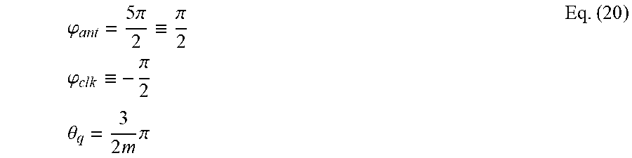


XML
uspto.report is an independent third-party trademark research tool that is not affiliated, endorsed, or sponsored by the United States Patent and Trademark Office (USPTO) or any other governmental organization. The information provided by uspto.report is based on publicly available data at the time of writing and is intended for informational purposes only.
While we strive to provide accurate and up-to-date information, we do not guarantee the accuracy, completeness, reliability, or suitability of the information displayed on this site. The use of this site is at your own risk. Any reliance you place on such information is therefore strictly at your own risk.
All official trademark data, including owner information, should be verified by visiting the official USPTO website at www.uspto.gov. This site is not intended to replace professional legal advice and should not be used as a substitute for consulting with a legal professional who is knowledgeable about trademark law.