Semiconductor Device and Method of Forming Conductive Vias to Have Enhanced Contact to Shielding Layer
Kim; SungSoo ; et al.
U.S. patent application number 15/955014 was filed with the patent office on 2019-10-17 for semiconductor device and method of forming conductive vias to have enhanced contact to shielding layer. This patent application is currently assigned to STATS ChipPAC Pte. Ltd.. The applicant listed for this patent is STATS ChipPAC Pte. Ltd.. Invention is credited to DaeHyeok Ha, SungSoo Kim, SangMi Park.
| Application Number | 20190318984 15/955014 |
| Document ID | / |
| Family ID | 68162137 |
| Filed Date | 2019-10-17 |


View All Diagrams
| United States Patent Application | 20190318984 |
| Kind Code | A1 |
| Kim; SungSoo ; et al. | October 17, 2019 |
Semiconductor Device and Method of Forming Conductive Vias to Have Enhanced Contact to Shielding Layer
Abstract
A semiconductor device has a substrate with a plurality of conductive vias formed through the substrate in an offset pattern. An electrical component is disposed in a die attach area over a first surface of the substrate. The conductive vias are formed around the die attach area of the substrate. A first conductive layer is formed over the first surface of the substrate, and a second conductive layer is formed over the second surface. An encapsulant is deposited over the substrate and electrical component. The substrate is singulated through the conductive vias. A first conductive via has a greater exposed surface area than a second conductive via. A shielding layer is formed over the electrical component and in contact with a side surface of the conductive vias. The shielding layer may extend over a second surface of substrate opposite the first surface of the substrate.
| Inventors: | Kim; SungSoo; (Seoul, KR) ; Ha; DaeHyeok; (Incheon-si, KR) ; Park; SangMi; (Incheon, KR) | ||||||||||
| Applicant: |
|
||||||||||
|---|---|---|---|---|---|---|---|---|---|---|---|
| Assignee: | STATS ChipPAC Pte. Ltd. Singapore SG |
||||||||||
| Family ID: | 68162137 | ||||||||||
| Appl. No.: | 15/955014 | ||||||||||
| Filed: | April 17, 2018 |
| Current U.S. Class: | 1/1 |
| Current CPC Class: | H01L 2224/13116 20130101; H01L 23/49827 20130101; H01L 2224/11464 20130101; H01L 2224/131 20130101; H05K 1/0216 20130101; H01L 23/49838 20130101; H01L 2224/11462 20130101; H01L 2224/05644 20130101; H01L 24/16 20130101; H01L 2224/13124 20130101; H01L 2224/13155 20130101; H01L 2224/81411 20130101; H01L 2224/05639 20130101; H01L 2224/05624 20130101; H05K 3/0052 20130101; H01L 23/15 20130101; H01L 24/13 20130101; H01L 2224/81455 20130101; H01L 2924/3025 20130101; H01L 2224/81439 20130101; H01L 2224/81444 20130101; H01L 23/552 20130101; H01L 23/49805 20130101; H01L 2924/141 20130101; H01L 2924/18161 20130101; H05K 3/403 20130101; H01L 2224/13147 20130101; H01L 2224/11334 20130101; H01L 2224/81466 20130101; H01L 2224/81484 20130101; H01L 2924/181 20130101; H01L 2224/05647 20130101; H01L 2224/13111 20130101; H01L 2224/94 20130101; H01L 2924/15311 20130101; H01L 2224/81447 20130101; H01L 24/17 20130101; H01L 2224/81191 20130101; H01L 2224/0401 20130101; H01L 23/145 20130101; H01L 2224/03452 20130101; H01L 2224/0346 20130101; H01L 2224/11849 20130101; H01L 2924/15313 20130101; H01L 2224/05655 20130101; H01L 2224/16235 20130101; H01L 2924/01006 20130101; H01L 2224/0345 20130101; H01L 2224/1134 20130101; H01L 2224/13144 20130101; H01L 2224/81815 20130101; H01L 24/05 20130101; H01L 2224/81424 20130101; H01L 2224/05611 20130101; H01L 2224/13139 20130101; H01L 2224/1132 20130101; H01L 2224/13113 20130101; H01L 2224/16237 20130101; H01L 2924/01013 20130101; H01L 2224/0345 20130101; H01L 2924/00014 20130101; H01L 2224/03452 20130101; H01L 2924/00014 20130101; H01L 2224/0346 20130101; H01L 2924/00014 20130101; H01L 2224/1132 20130101; H01L 2924/00014 20130101; H01L 2224/11334 20130101; H01L 2924/00014 20130101; H01L 2224/11462 20130101; H01L 2924/00014 20130101; H01L 2224/11464 20130101; H01L 2924/00014 20130101; H01L 2224/11849 20130101; H01L 2924/00014 20130101; H01L 2224/1134 20130101; H01L 2924/00014 20130101; H01L 2224/94 20130101; H01L 2224/11 20130101; H01L 2224/94 20130101; H01L 2224/03 20130101; H01L 2224/81815 20130101; H01L 2924/00014 20130101; H01L 2224/131 20130101; H01L 2924/014 20130101; H01L 2924/00014 20130101; H01L 2224/13111 20130101; H01L 2924/01322 20130101; H01L 2924/01082 20130101; H01L 2924/00014 20130101; H01L 2224/13116 20130101; H01L 2924/01322 20130101; H01L 2924/0105 20130101; H01L 2924/00014 20130101; H01L 2224/05639 20130101; H01L 2924/00014 20130101; H01L 2224/05624 20130101; H01L 2924/00014 20130101; H01L 2224/05644 20130101; H01L 2924/00014 20130101; H01L 2224/05611 20130101; H01L 2924/00014 20130101; H01L 2224/81439 20130101; H01L 2924/013 20130101; H01L 2924/00014 20130101; H01L 2224/05647 20130101; H01L 2924/00014 20130101; H01L 2224/81484 20130101; H01L 2924/013 20130101; H01L 2924/01022 20130101; H01L 2924/00014 20130101; H01L 2224/81466 20130101; H01L 2924/013 20130101; H01L 2924/01074 20130101; H01L 2924/00014 20130101; H01L 2224/13155 20130101; H01L 2924/013 20130101; H01L 2924/00014 20130101; H01L 2224/81424 20130101; H01L 2924/013 20130101; H01L 2924/00014 20130101; H01L 2224/81444 20130101; H01L 2924/013 20130101; H01L 2924/00014 20130101; H01L 2224/13124 20130101; H01L 2924/013 20130101; H01L 2924/00014 20130101; H01L 2224/13139 20130101; H01L 2924/013 20130101; H01L 2924/00014 20130101; H01L 2224/13144 20130101; H01L 2924/013 20130101; H01L 2924/00014 20130101; H01L 2224/81455 20130101; H01L 2924/013 20130101; H01L 2924/00014 20130101; H01L 2224/81411 20130101; H01L 2924/013 20130101; H01L 2924/00014 20130101; H01L 2224/05655 20130101; H01L 2924/00014 20130101; H01L 2224/81447 20130101; H01L 2924/013 20130101; H01L 2924/00014 20130101; H01L 2224/13113 20130101; H01L 2924/013 20130101; H01L 2924/00014 20130101; H01L 2224/13147 20130101; H01L 2924/013 20130101; H01L 2924/00014 20130101 |
| International Class: | H01L 23/498 20060101 H01L023/498; H01L 23/00 20060101 H01L023/00; H01L 23/552 20060101 H01L023/552; H05K 1/02 20060101 H05K001/02 |
Claims
1. A method of making a semiconductor device, comprising: providing a substrate including a first conductive via formed through the substrate and a second conductive via formed through the substrate adjacent to the first conductive via, wherein a centerline of the first conductive via is offset with respect to a centerline of the second conductive via; disposing an electrical component in a die attach area over a first surface of the substrate; singulating the substrate through the first conductive via and second conductive via; and forming a shielding layer over the electrical component and in contact with a side surface of the first conductive via and second conductive via.
2. The method of claim 1, further including depositing an encapsulant over the substrate and electrical component.
3. A method of making a semiconductor device, comprising: providing a substrate including a first conductive via formed through the substrate and a second conductive via formed through the substrate adjacent to the first conductive via, wherein the first conductive via is offset with respect to the second conductive via; disposing an electrical component in a die attach area over a first surface of the substrate; singulating the substrate through the first conductive via and second conductive via; and forming a shielding layer over the electrical component and in contact with a side surface of the first conductive via and second conductive via, wherein the side surface of the first conductive via has a greater exposed surface area than the side surface of the second conductive via.
4. The method of claim 1, wherein the shielding layer extends over a second surface of substrate opposite the first surface of the substrate.
5. The method of claim 1, further including forming a conductive layer over a second surface of substrate opposite the first surface of the substrate, wherein the conductive layer includes a plurality of gaps.
6. The method of claim 1, further including forming a plurality of conductive vias around the die attach area of the substrate.
7. A method of making a semiconductor device, comprising: providing a substrate including a plurality of conductive vias formed through the substrate in an offset pattern along a centerline; disposing an electrical component in a die attach area over a first surface of the substrate; singulating the substrate through the conductive vias; and forming a shielding layer over the electrical component and in contact with a side surface of the conductive vias.
8. The method of claim 7, further including depositing an encapsulant over the substrate and electrical component.
9. The method of claim 7, wherein a first conductive via of the plurality of conductive vias has a greater exposed surface area than a second conductive via of the plurality of conductive vias.
10. The method of claim 7, wherein the shielding layer extends over a second surface of substrate opposite the first surface of the substrate.
11. The method of claim 7, further including forming a conductive layer over a second surface of substrate opposite the first surface of the substrate, wherein the conductive layer includes a plurality of gaps.
12. The method of claim 7, further including forming a conductive layer over the first surface of the substrate.
13. The method of claim 7, further including forming the plurality of conductive vias around the die attach area of the substrate.
14. A method of making a semiconductor device, comprising: providing a substrate including a plurality of conductive vias having a rectangular form extending through the substrate; disposing an electrical component in a die attach area over a first surface of the substrate; singulating the substrate through the conductive vias; and forming a shielding layer over the electrical component and in contact with a side surface of the conductive vias.
15. The method of claim 14, further including depositing an encapsulant over the substrate and electrical component.
16. The method of claim 14, wherein the shielding layer extends over a second surface of substrate opposite the first surface of the substrate.
17. The method of claim 14, further including forming a conductive layer over a second surface of substrate opposite the first surface of the substrate, wherein the conductive layer includes a plurality of gaps.
18. The method of claim 14, further including forming a conductive layer over the first surface of the substrate.
19. The method of claim 14, further including forming the plurality of conductive vias around the die attach area of the substrate.
20. A semiconductor device, comprising: a substrate including a plurality of conductive vias formed through the substrate in an offset pattern along a centerline; an electrical component disposed in a die attach area over a first surface of the substrate, wherein the substrate is singulated through the conductive vias; and a shielding layer formed over the electrical component and in contact with a side surface of the conductive vias.
21. The semiconductor device of claim 20, further including an encapsulant deposited over the substrate and electrical component.
22. The semiconductor device of claim 20, wherein a first conductive via of the plurality of conductive vias has a greater exposed surface area than a second conductive via of the plurality of conductive vias.
23. The semiconductor device of claim 20, wherein the shielding layer extends over a second surface of substrate opposite the first surface of the substrate.
24. The semiconductor device of claim 20, further including forming a conductive layer over a second surface of substrate opposite the first surface of the substrate, wherein the conductive layer includes a plurality of gaps.
25. The semiconductor device of claim 20, further including forming the plurality of conductive vias around the die attach area of the substrate.
Description
FIELD OF THE INVENTION
[0001] The present invention relates in general to semiconductor devices and, more particularly, to a semiconductor device and method of forming conductive vias to have enhanced contact with a shielding layer.
BACKGROUND OF THE INVENTION
[0002] Semiconductor devices are commonly found in modern electronic products. Semiconductor devices perform a wide range of functions such as signal processing, high-speed calculations, transmitting and receiving electromagnetic signals, controlling electronic devices, photo-electric, and creating visual images for television displays. Semiconductor devices are found in the fields of communications, power conversion, networks, computers, entertainment, and consumer products. Semiconductor devices are also found in military applications, aviation, automotive, industrial controllers, and office equipment.
[0003] Semiconductor devices, particularly in high frequency applications such as radio frequency (RF) wireless communications, often contain one or more integrated passive devices (IPDs) to perform necessary electrical functions. The IPDs are susceptible to electromagnetic interference (EMI), radio frequency interference (RFI), harmonic distortion, or other inter-device interference, such as capacitive, inductive, or conductive coupling, also known as cross-talk, which can interfere with their operation. The high-speed switching of digital circuits also generate interference.
[0004] A semiconductor die and/or discrete IPD can be integrated into a semiconductor package. The semiconductor die and discrete IPDs are mounted to a substrate panel for structural support and electrical interconnect. An encapsulant is deposited over the semiconductor die, discrete IPDs, and substrate panel. A shielding layer is formed over the encapsulant to isolate EMI/RFI sensitive circuits. Conductive vias can be formed through the substrate panel for electrical interconnect, including the ground connection to the shielding layer. The conductive vias are cylindrical and laid out in a linear arrangement, i.e., lined up with a center point of each via along a straight line.
[0005] The substrate panel is singulated through the conductive vias so that the shielding layer can make contact with an exposed side surface of the singulated conductive vias. Singulation has some variance in the cutting alignment, direction, and angle. If the conductive vias are singulated off-center, then the cylinders are not cut into ideal half cylinders, but rather have a fraction (less than half) of the cylinder as the exposed side surface of the singulated conductive vias. The less than half fractional cylinder has a reduced vertical surface area (compared to a half cylinder from an ideal cut) of the conducive vias to make contact to the shielding layer. The reduced contact surface area can adversely affect the function of the shielding layer with a poor ground contact and less adhesive integrity to the conductive vias.
BRIEF DESCRIPTION OF THE DRAWINGS
[0006] FIGS. 1a-1c illustrate a semiconductor wafer with a plurality of semiconductor die separated by a saw street;
[0007] FIGS. 2a-2b illustrate a prefabricated interconnect substrate panel;
[0008] FIGS. 3a-3e illustrate a process of forming a semiconductor package using the substrate panel with staggered conductive vias;
[0009] FIGS. 4a-4e illustrate singulation of the staggered conductive vias with cutting variance;
[0010] FIGS. 5a-5e illustrate singulation of rectangular conductive vias with cutting variance;
[0011] FIGS. 6a-6b illustrate singulation of rhombus conductive vias;
[0012] FIGS. 7a-7b illustrate singulation of hexagon conductive vias;
[0013] FIG. 8 illustrates the semiconductor package according to FIGS. 3a-3e with a shielding layer connected to a side surface of the staggered conductive vias;
[0014] FIGS. 9a-9b illustrate another process of forming the semiconductor package with a shielding layer;
[0015] FIGS. 10a-10d illustrate a process of forming a semiconductor package using the substrate panel with a repeating pattern of gear-tooth shaped conductive layer;
[0016] FIG. 11 illustrates the semiconductor package according to FIGS. 10a-10c with a shielding layer connected to a side surface of the rectangular conductive vias;
[0017] FIG. 12 illustrates the semiconductor package with the shielding layer extending over a bottom conductive layer; and
[0018] FIG. 13 illustrates a printed circuit board (PCB) with different types of packages mounted to a surface of the PCB.
DETAILED DESCRIPTION OF THE DRAWINGS
[0019] The present invention is described in one or more embodiments in the following description with reference to the figures, in which like numerals represent the same or similar elements. While the invention is described in terms of the best mode for achieving the invention's objectives, it will be appreciated by those skilled in the art that it is intended to cover alternatives, modifications, and equivalents as may be included within the spirit and scope of the invention as defined by the appended claims and their equivalents as supported by the following disclosure and drawings. The term "semiconductor die" as used herein refers to both the singular and plural form of the words, and accordingly, can refer to both a single semiconductor device and multiple semiconductor devices.
[0020] Semiconductor devices are generally manufactured using two complex manufacturing processes: front-end manufacturing and back-end manufacturing. Front-end manufacturing involves the formation of a plurality of die on the surface of a semiconductor wafer. Each die on the wafer contains active and passive electrical components, which are electrically connected to form functional electrical circuits. Active electrical components, such as transistors and diodes, have the ability to control the flow of electrical current. Passive electrical components, such as capacitors, inductors, and resistors, create a relationship between voltage and current necessary to perform electrical circuit functions.
[0021] Back-end manufacturing refers to cutting or singulating the finished wafer into the individual semiconductor die and packaging the semiconductor die for structural support, electrical interconnect, and environmental isolation. To singulate the semiconductor die, the wafer is scored and broken along non-functional regions of the wafer called saw streets or scribes. The wafer is singulated using a laser cutting tool or saw blade. After singulation, the individual semiconductor die are mounted to a package substrate that includes pins or contact pads for interconnection with other system components. Contact pads formed over the semiconductor die are then connected to contact pads within the package. The electrical connections can be made with conductive layers, bumps, stud bumps, conductive paste, or wirebonds. An encapsulant or other molding material is deposited over the package to provide physical support and electrical isolation. The finished package is then inserted into an electrical system and the functionality of the semiconductor device is made available to the other system components.
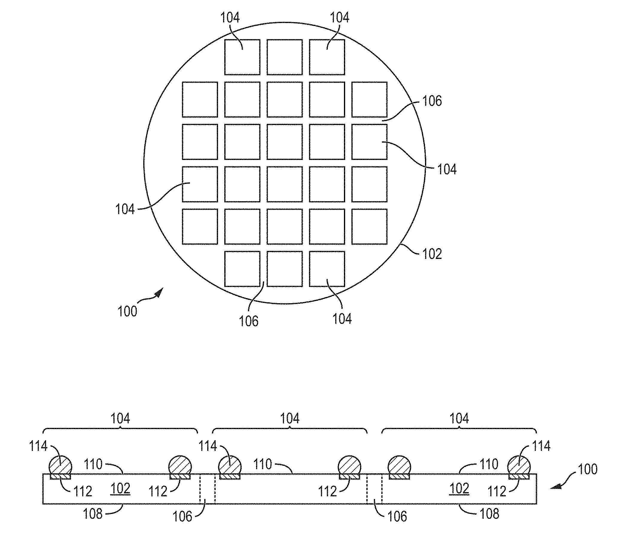
[0022] FIG. 1a shows a semiconductor wafer 100 with a base substrate material 102, such as silicon, germanium, aluminum phosphide, aluminum arsenide, gallium arsenide, gallium nitride, indium phosphide, silicon carbide, or other bulk material for structural support. A plurality of semiconductor die or components 104 is formed on wafer 100 separated by a non-active, inter-die wafer area or saw street 106. Saw street 106 provides cutting areas to singulate semiconductor wafer 100 into individual semiconductor die 104. In one embodiment, semiconductor wafer 100 has a width or diameter of 100-450 millimeters (mm).
[0023] FIG. 1b shows a cross-sectional view of a portion of semiconductor wafer 100. Each semiconductor die 104 has a back or non-active surface 108 and an active surface 110 containing analog or digital circuits implemented as active devices, passive devices, conductive layers, and dielectric layers formed within the die and electrically interconnected according to the electrical design and function of the die. For example, the circuit may include one or more transistors, diodes, and other circuit elements formed within active surface 110 to implement analog circuits or digital circuits, such as digital signal processor (DSP), application specific integrated circuits (ASIC), memory, or other signal processing circuit.
[0024] Semiconductor die 104 may also contain IPDs, such as inductors, capacitors, and resistors, for RF signal processing.
[0025] An electrically conductive layer 112 is formed over active surface 110 using PVD, CVD, electrolytic plating, electroless plating process, or other suitable metal deposition process. Conductive layer 112 can be one or more layers of aluminum (Al), copper (Cu), tin (Sn), nickel (Ni), gold (Au), silver (Ag), or other suitable electrically conductive material. Conductive layer 112 operates as contact pads electrically connected to the circuits on active surface 110.
[0026] An electrically conductive bump material is deposited over conductive layer 112 using an evaporation, electrolytic plating, electroless plating, ball drop, or screen printing process. The bump material can be Al, Sn, Ni, Au, Ag, Pb, Bi, Cu, solder, and combinations thereof, with an optional flux solution. For example, the bump material can be eutectic Sn/Pb, high-lead solder, or lead-free solder. The bump material is bonded to conductive layer 112 using a suitable attachment or bonding process. In one embodiment, the bump material is reflowed by heating the material above its melting point to form balls or bumps 114. In one embodiment, bump 114 is formed over an under bump metallization (UBM) having a wetting layer, barrier layer, and adhesive layer. Bump 114 can also be compression bonded or thermocompression bonded to conductive layer 112. Bump 114 represents one type of interconnect structure that can be formed over conductive layer 112. The interconnect structure can also use bond wires, conductive paste, stud bump, micro bump, or other electrical interconnect.
[0027] In FIG. 1c, semiconductor wafer 100 is singulated through saw street 106 using a saw blade or laser cutting tool 118 into individual semiconductor die 104. The individual semiconductor die 104 can be inspected and electrically tested for identification of known good die (KGD) post singulation.
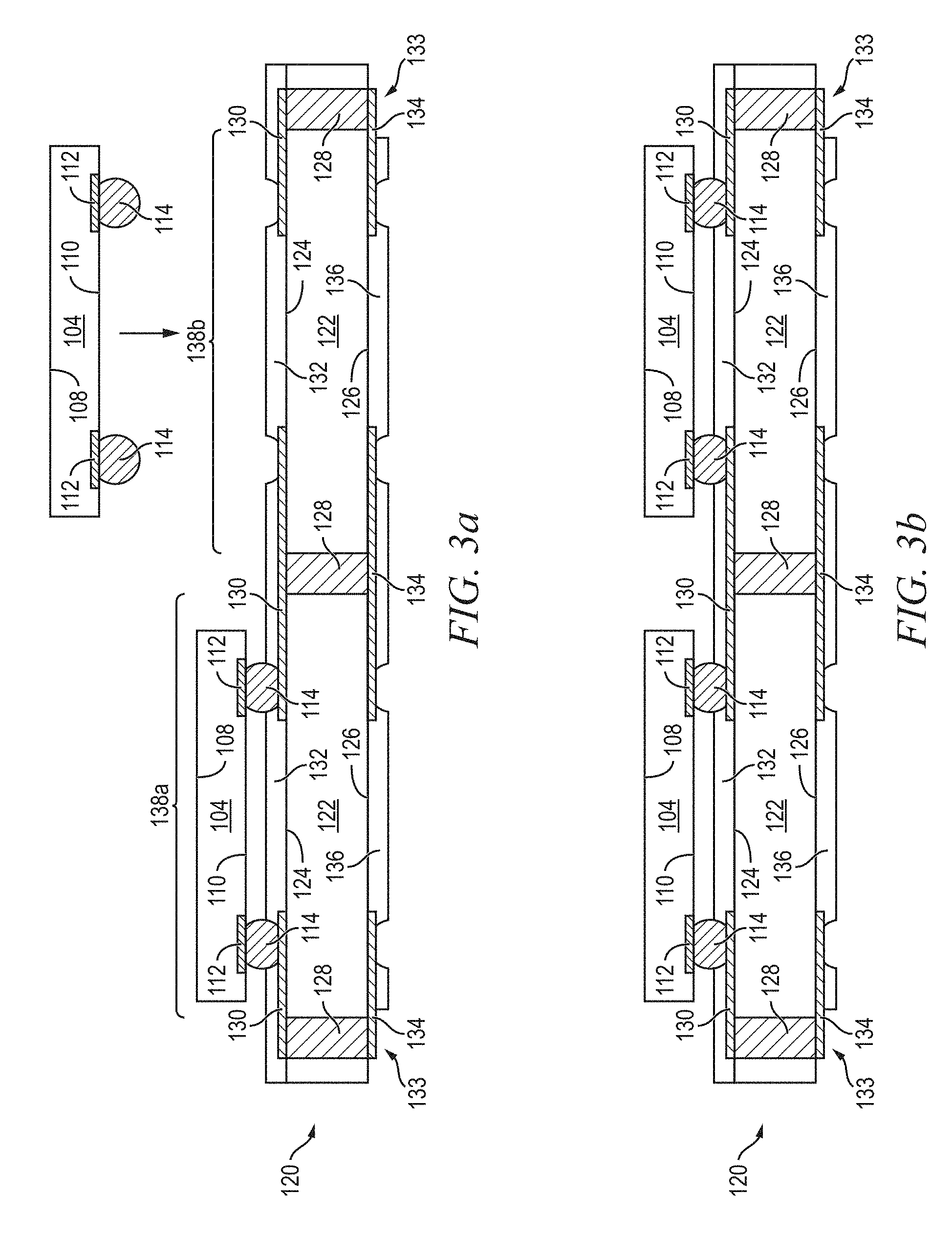
[0028] FIGS. 2a-2b illustrate a prefabricated interconnect substrate or interposer panel 120 including core substrate 122 having opposing surfaces 124 and 126. Core substrate 122 includes one or more insulating layers, such as silicon dioxide (SiO.sub.2), silicon nitride (Si.sub.3N.sub.4), silicon oxynitride (SiON), tantalum pentoxide (Ta.sub.2O.sub.5), aluminum oxide (Al.sub.2O.sub.3), solder resist, polyimide, benzocyclobutene (BCB), polybenzoxazoles (PBO), and other material having similar insulating and structural properties. Alternatively, core substrate 122 may include one or more laminated layers of polytetrafluoroethylene pre-impregnated (prepreg), FR-4, FR-1, CEM-1, or CEM-3 with a combination of phenolic cotton paper, epoxy, resin, woven glass, matte glass, polyester, and other reinforcement fibers or fabrics.
[0029] A plurality of through vias is formed through core substrate 122 using laser drilling, mechanical drilling, deep reactive ion etching (DRIE), or other suitable process. The through vias extend completely through core substrate 122 from surface 124 to surface 126. The through vias are filled with Al, Cu, Sn, Ni, Au, Ag, Ti, TiW, W, or other suitable electrically conductive material or combination thereof using PVD, CVD, electrolytic plating, electroless plating process, or other suitable metal deposition process to form z-direction vertical interconnect structures or conductive vias 128.
[0030] A conductive layer 130 is formed over surface 124 of core substrate 122 using PVD, CVD, electrolytic plating, electroless plating process, or other suitable metal deposition. Conductive layer 130 includes one or more layers of Al, Cu, Sn, Ni, Au, Ag, Ti, TiW, W, or other suitable electrically conductive material or combination thereof. Portions of conductive layer 130 operate as contact pads and are electrically connected to conductive vias 128. Conductive layer 130 also includes portions that are electrically common or electrically isolated depending on the routing design and function of the semiconductor package. In one embodiment, conductive layer 130 operates as an RDL extending electrical connection from conductive vias 128 to areas adjacent to conductive vias 128 to laterally redistribute electrical signals across substrate panel 120.
[0031] An insulating or passivation layer 132 is formed over surface 124 of core substrate 122 and conductive layer 130 using PVD, CVD, printing, lamination, spin coating, spray coating, sintering, or thermal oxidation. The insulating layer 132 contains one or more layers of SiO.sub.2, Si.sub.3N.sub.4, SiON, Ta.sub.2O.sub.5, Al.sub.2O.sub.3, polymer dielectric resist with or without fillers or fibers, or other material having similar insulating and structural properties. In one embodiment, insulating layer 132 is a solder resist layer. A portion of insulating layer 132 is removed by LDA, etching, or other suitable process to expose portions of conductive layer 130.
[0032] A conductive layer 134 is formed over surface 126 of core substrate 122 using PVD, CVD, electrolytic plating, electroless plating process, or other suitable metal deposition. Conductive layer 134 includes one or more layers of Al, Cu, Sn, Ni, Au, Ag, Ti, TiW, W, or other suitable electrically conductive material or combination thereof. Portions of conductive layer 134 operate as contact pads and are electrically connected to conductive vias 128. Conductive layer 134 also may include portions that are electrically common or electrically isolated depending on the routing design and function of the semiconductor package. Alternatively, conductive vias 128 are formed through core substrate 122 after forming conductive layers 130 and 134.
[0033] An insulating or passivation layer 136 is formed over surface 126 of core substrate 122 and conductive layer 134 using PVD, CVD, printing, lamination, spin coating, spray coating, sintering, or thermal oxidation. The insulating layer 136 contains one or more layers of SiO.sub.2, Si.sub.3N.sub.4, SiON, Ta.sub.2O.sub.5, Al.sub.2O.sub.3, polymer dielectric resist with or without fillers or fibers, or other material having similar insulating and structural properties. In one embodiment, insulating layer 136 is a solder resist layer. Portions of conductive layer 134 can be arranged in a repeating side-by-side rectangular pattern with an opening through insulating layer 136 to expose the conductive layer as a ground contact. A portion of insulating layer 136 is removed by LDA, etching, or other suitable process to expose portions of conductive layer 134, as well as areas 133 proximate to the connection between conductive layer 134 and conductive vias 128. Areas 133 with no insulating layer 136 extend around a perimeter of substrate panel 120 to provide external ground connection.
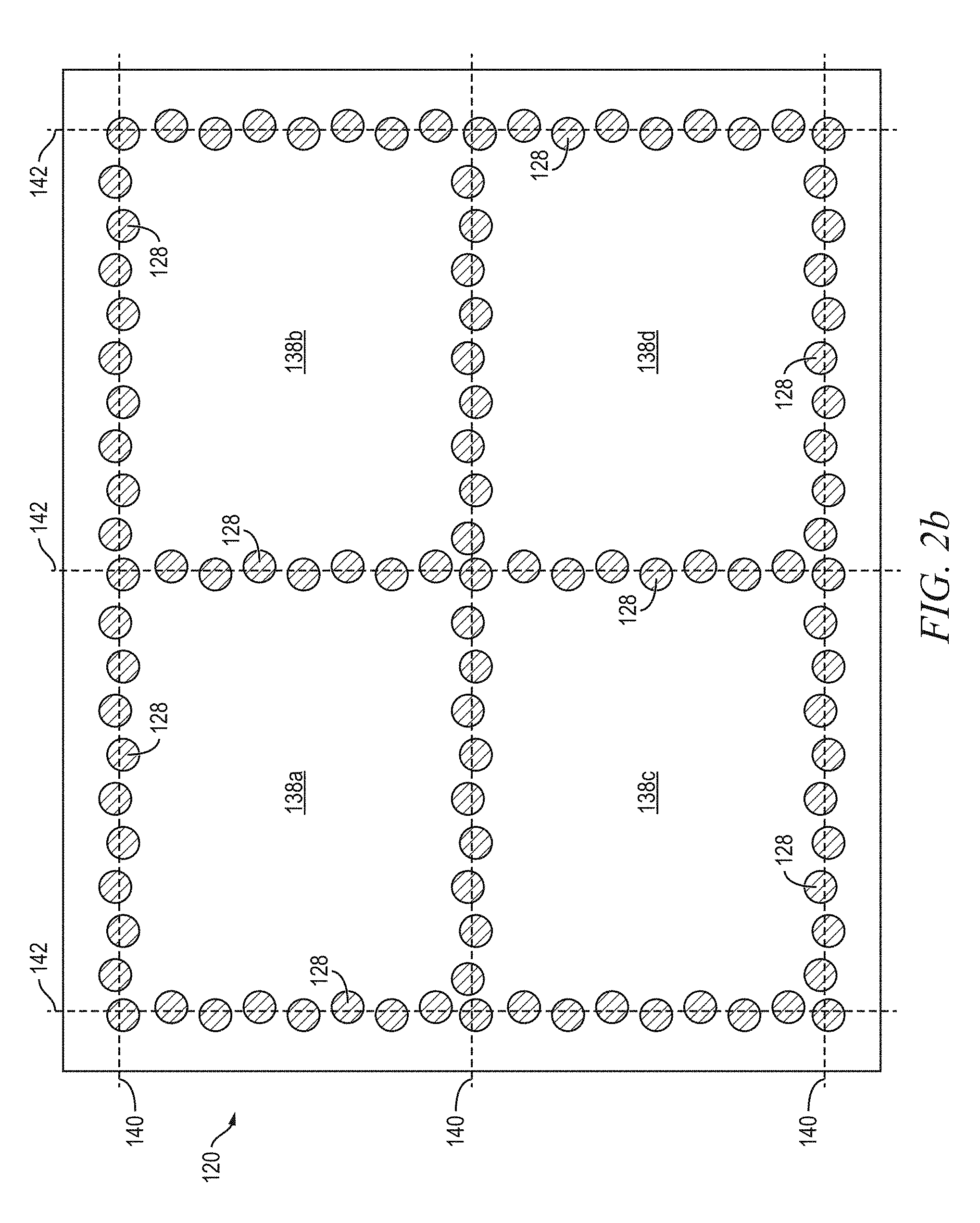
[0034] FIG. 2b is a plane view of substrate panel 120 with sufficient surface area to contain multiple semiconductor die 104. Each die attach areas 138a-138d is designated for placement of at least one semiconductor die 104. Conductive vias 128 are arranged in a staggered or offset pattern completely around a perimeter of each die attachment area 138a-138d. Substrate panel 120 will be singulated through dicing lines 140 and 142. The staggered or offset pattern of conductive vias 128 provides enhanced contact surface area along the vertical side surface post singulation, given variance during cutting along dicing lines 140 and 142.
[0035] FIGS. 3a-3e illustrate a process of forming a semiconductor package using substrate panel 120 with staggered conductive vias 128. In FIG. 3a, semiconductor die 104 from FIG. 1c is positioned over each die attach area 138a-138d of substrate panel 120 using a pick and place operation with active surface 110 and bumps 114 oriented toward surface 124. FIG. 3b shows semiconductor die 104 bonded to conductive layer 130 within die attach areas 138a-138d of substrate panel 120 by reflowing bumps 114. FIG. 3c shows a plan view of semiconductor die 104 bonded to substrate panel 120 with conductive vias 128 disposed around a perimeter of each semiconductor die. Semiconductor die 104 represents one type of semiconductor device or electrical component that can be disposed over die attach areas 138a-138d of substrate panel 120. Other semiconductor or electrical components include a semiconductor package, semiconductor module, and discrete electrical device, such as a resistor, capacitor, and inductor.
[0036] In FIG. 3d, an encapsulant or molding compound 150 is deposited over semiconductor die 104 and substrate panel 120 using a paste printing, compressive molding, transfer molding, liquid encapsulant molding, vacuum lamination, spin coating, or other suitable applicator. Encapsulant 150 can be polymer composite material, such as epoxy resin with filler, epoxy acrylate with filler, or polymer with proper filler.
[0037] Encapsulant 150 is non-conductive, provides structural support, and environmentally protects the semiconductor device from external elements and contaminants.
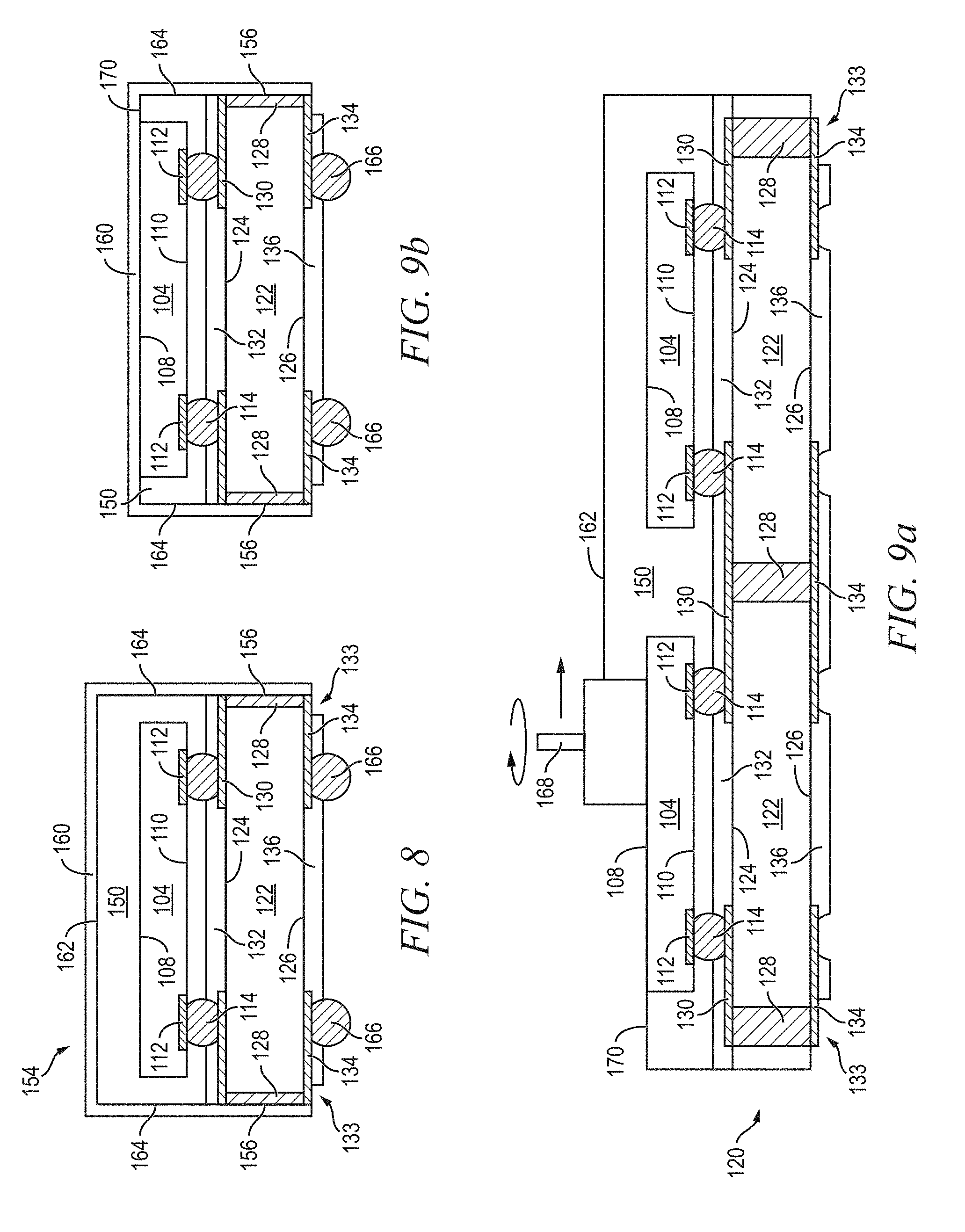
[0038] In FIG. 3e, semiconductor panel 120 is singulated through conductive vias 128 along dicing lines 140 and 142, see FIG. 2b, using a saw blade or laser cutting tool 152 into individual semiconductor packages 154. The singulation process has variance and tolerances of the cutting path. The staggered or offset pattern of conductive vias 128 provides enhanced contact surface area along vertical side surface 156 post singulation, given variance during cutting along dicing lines 140 and 142.
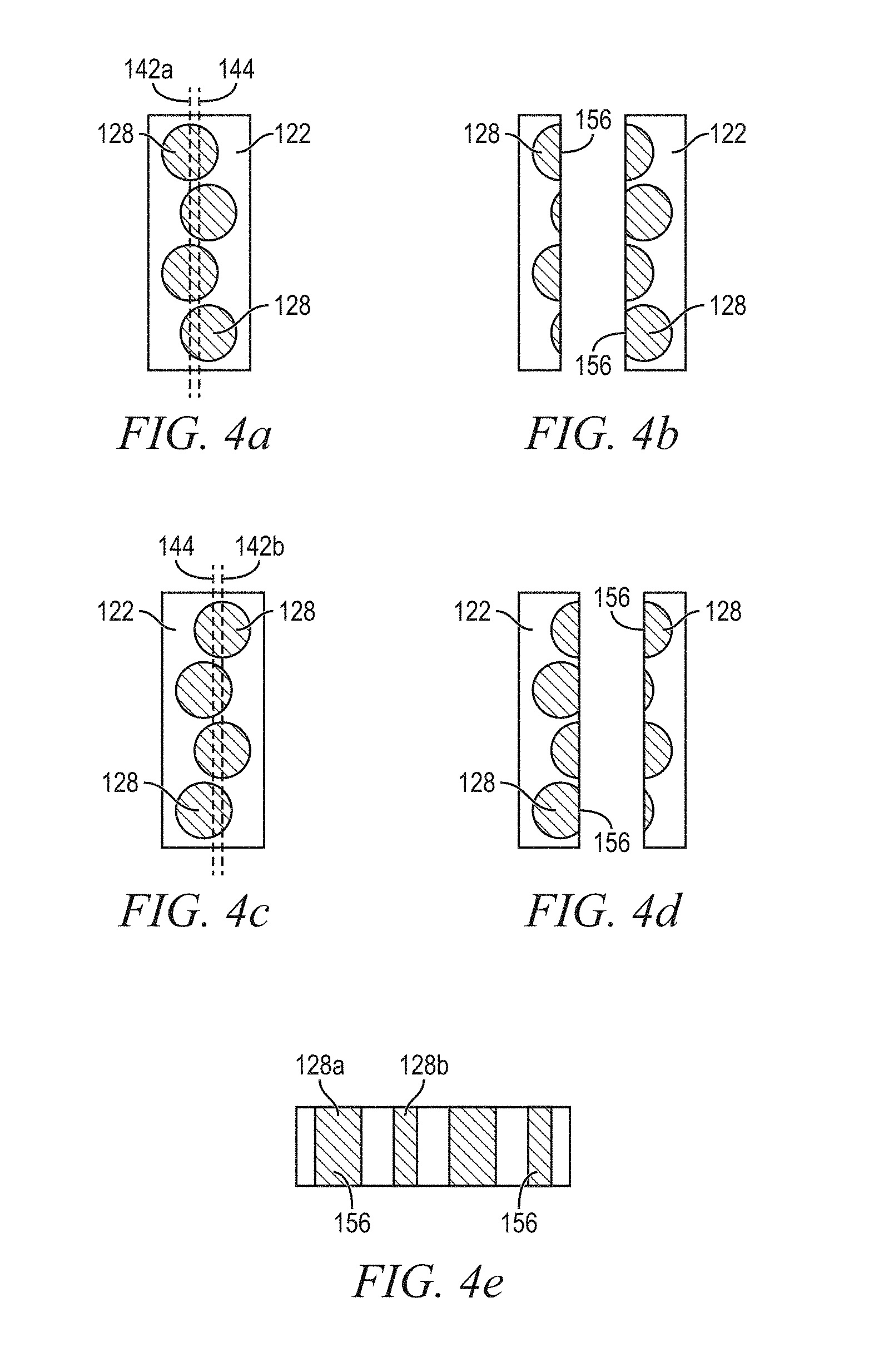
[0039] FIGS. 4a-4e illustrate further detail of singulation through conductive vias 128 arranged in the staggered or offset pattern around die attachment areas 138a-138d. In FIG. 4a, dicing line 142a is to the left of an ideal centerline 144 through conductive vias 128, due to the cutting variance. FIG. 4b shows the post singulation along dicing line 142a. In FIG. 4c, dicing line 142b is to the right of an ideal centerline 144 through conductive vias 128, again due to the cutting variance. FIG. 4d shows the post singulation along dicing line 142b. The same feature is achieved along dicing lines 140. In each case, the staggered or offset pattern of conductive vias 128 provides enhanced contact surface area along vertical side surface 156 post singulation, given variance during cutting along dicing lines 140 and 142. FIG. 4e shows a side view of core substrate 122 and conductive vias 128 with vertical contact side surface 156 post singulation.
[0040] The staggered or offset pattern of conductive vias 128 provides enhanced contact surface area along vertical side surface 156 to shielding layer 160, given variance during cutting along dicing lines 140 and 142. In fact, the total contact area between vertical side surfaces 156 and shielding layer 160 remains substantially uniform and constant, independent of singulation location within a tolerance of centerline 144. The enhanced contact surface area along vertical side surface 156 improves adhesion between conductive vias 128 and shielding layer 160, as well as effectiveness of electrical properties of the shielding layer. With the cylindrical form-factor and offset or staggered pattern, conductive via 128a has a greater exposed side surface area 156 than the adjacent conductive via 128b. Some conductive vias 128 have more exposed side surface area, some conductive vias 128 have less exposed side surface area. The total exposed side surface area 156 among multiple conductive vias 128 remains unchanged, independent of the dicing location within a tolerance of centerline 144.
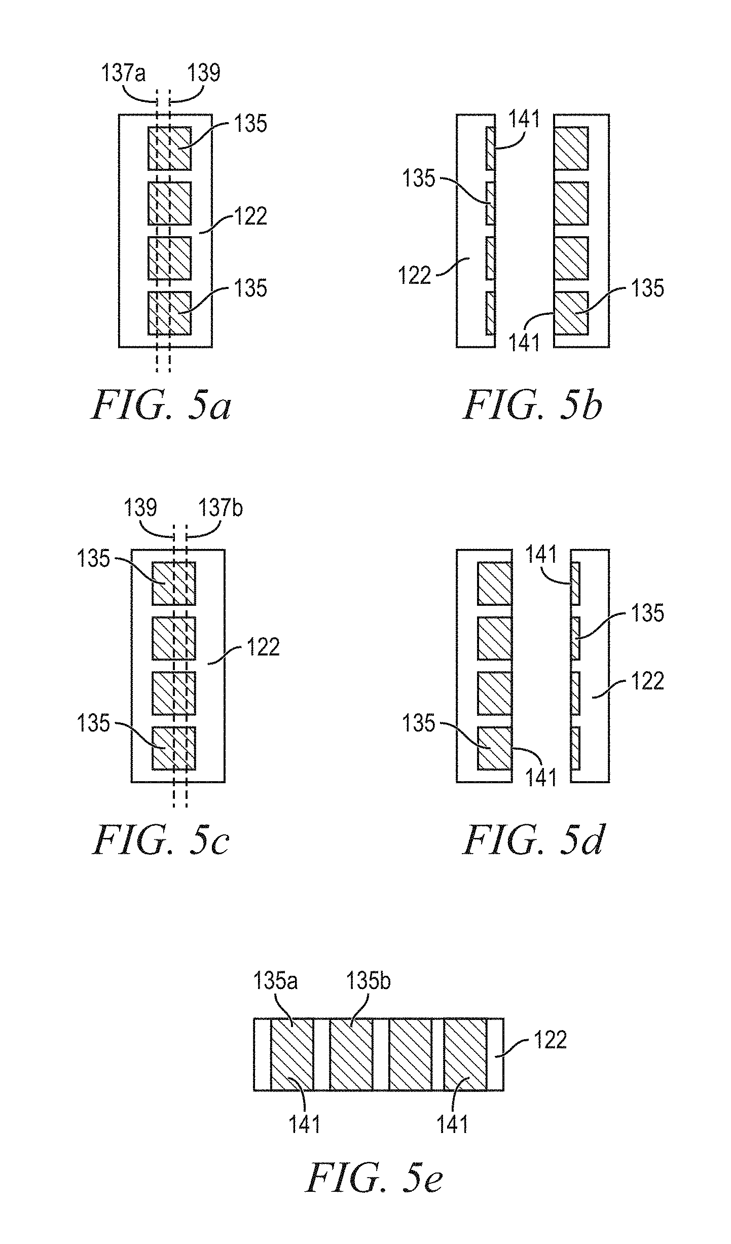
[0041] FIGS. 5a-5e illustrate further detail of singulation through rectangular conductive vias 135 arranged in the repeating side-by-side pattern around die attachment area 138a-138d. In FIG. 5a, dicing line 137a is to the left of an ideal centerline 139 through conductive vias 135, due to the cutting variance. FIG. 5b shows the post singulation along dicing line 137a. In FIG. 5c, dicing line 137b is to the right of an ideal centerline 139 through conductive vias 135, again due to the cutting variance. FIG. 5d shows the post singulation along dicing line 137a. The repeating side-by-side pattern of rectangular conductive vias 135 provides enhanced contact surface area along vertical side surface 141 post singulation, given variance during cutting along dicing lines 137a-137b. In other words, the vertical side surface area 141 of rectangular conductive vias 135 is the same, independent of variance during cutting along dicing lines 137a-137b. FIG. 5e shows a side view of core substrate 122 and conductive vias 135 with vertical contact side surface 141 post singulation.
[0042] FIGS. 6a-6b illustrate further detail of singulation through rhombus-shaped conductive vias 146 arranged in the staggered or offset pattern around die attachment areas 138a-138d. In FIG. 6a, conductive vias 146 are cut along dicing line 147. FIG. 6b shows the post singulation along dicing line 147. The staggered or offset pattern of conductive vias 146 provides enhanced contact surface area along vertical side surface 148 to shielding layer 160, given variance during cutting along dicing line 147. In fact, the total contact area between vertical side surfaces 148 and shielding layer 160 remains substantially uniform and constant. The enhanced contact surface area along vertical side surface 148 improves adhesion between conductive vias 146 and shielding layer 160, as well as effectiveness of electrical properties of the shielding layer.
[0043] FIGS. 7a-7b illustrate further detail of singulation through hexagon-shaped conductive vias 157 arranged in the staggered or offset pattern around die attachment areas 138a-138d. In FIG. 7a, conductive vias 157 are cut along dicing line 158. FIG. 7b shows the post singulation along dicing line 158. The staggered or offset pattern of conductive vias 157 provides enhanced contact surface area along vertical side surface 159 to shielding layer 160, given variance during cutting along dicing line 158. In fact, the total contact area between vertical side surfaces 159 and shielding layer 160 remains substantially uniform and constant. The enhanced contact surface area along vertical side surface 159 improves adhesion between conductive vias 157 and shielding layer 160, as well as effectiveness of electrical properties of the shielding layer.
[0044] The rhombus shaped conductive vias 146 and hexagon shaped conductive vias 157 in FIGS. 6-7 can reduce damage during mechanical sawing. Mechanical sawing is stable and low cost method for singulation. However, the mechanical saw causes shear stress into the rigid material, particularly metal such as via or conductive layer. The shear stress can result in delamination or other failure. The rhombus or hexagon pattern has less curvature than a circle and reduces shear stress.
[0045] Semiconductor die 104 may contain IPDs that are susceptible to or generate EMI, RFI, harmonic distortion, and inter-device interference. For example, the IPDs contained within semiconductor die 104 provide the electrical characteristics needed for high-frequency applications, such as resonators, high-pass filters, low-pass filters, band-pass filters, symmetric Hi-Q resonant transformers, and tuning capacitors. In another embodiment, semiconductor die 104 contains digital circuits switching at a high frequency, which could interfere with the operation of IPDs in nearby semiconductor packages.
[0046] In FIG. 8, shielding layer 160 is formed over surfaces 162 and 164 of encapsulant 150, using for example a sputtering process. Shielding layer 160 can be one or more layers of Al, Cu, Sn, Ni, Au, Ag, or other suitable conductive material. Alternatively, shielding layer 160 can be carbonyl iron, stainless steel, nickel silver, low-carbon steel, silicon-iron steel, foil, conductive resin, carbon-black, aluminum flake, and other metals and composites capable of reducing the effects of EMI, RFI, and other inter-device interference.
[0047] The staggered or offset pattern of conductive vias 128 provides enhanced contact surface area along vertical side surface 156 to shielding layer 160, given variance during cutting along dicing lines 140 and 142. In fact, the total contact area between vertical side surfaces 156 and shielding layer 160 remains substantially uniform and constant, independent of singulation location within a tolerance of centerline 144. The enhanced contact surface area along vertical side surface 156 improves adhesion between conductive vias 128 and shielding layer 160, as well as effectiveness of electrical properties of the shielding layer. With the cylindrical form-factor and offset or staggered pattern, some conductive vias 128 have more exposed side surface area, some conductive vias 128 have less exposed side surface area. The total exposed side surface area 156 among multiple conductive vias 128 remains unchanged, independent of the dicing location within a tolerance of centerline 144. The shapes of conductive vias 135, 146, or 157 can also be used to attach shielding layer 160.
[0048] An electrically conductive bump material is deposited over conductive layer 134 using an evaporation, electrolytic plating, electroless plating, ball drop, or screen printing process. The bump material can be Al, Sn, Ni, Au, Ag, Pb, Bi, Cu, solder, and combinations thereof, with an optional flux solution. For example, the bump material can be eutectic Sn/Pb, high-lead solder, or lead-free solder. The bump material is bonded to conductive layer 134 using a suitable attachment or bonding process. In one embodiment, the bump material is reflowed by heating the material above its melting point to form balls or bumps 166. In one embodiment, bump 166 is formed over a UBM having a wetting layer, barrier layer, and adhesive layer. Bump 166 can also be compression bonded or thermocompression bonded to conductive layer 134. Bump 166 represents one type of interconnect structure that can be formed over conductive layer 134. The interconnect structure can also use bond wires, conductive paste, stud bump, micro bump, or other electrical interconnect.
[0049] Shielding layer 160 makes contact to an external ground through conductive vias 128 and conductive layer 134 in area 133. Alternatively, shielding layer 160 can make contact to an external ground through conductive vias 128, conductive layer 134, and bumps 166. Semiconductor die 104 makes functional signal contact with external components through conductive layer 130, conductive vias 128, conductive layer 134, and bumps 166.
[0050] FIG. 9a shows a portion of encapsulant 150 removed by grinder 168 to expose back surface 108 of semiconductor die 104. Grinder 168 further planarizes surface 170 of encapsulant 150. Alternatively, a portion of encapsulant 150 is removed by an etching process or LDA to planarize surfaces 170 and expose back surface 108 of semiconductor die 104. In FIG. 9b, shielding layer 160 is formed over surfaces 170 and 164 of encapsulant 150 and back surface 108 of semiconductor die 104. Bump 166 is formed over conductive layer 134, as described above.
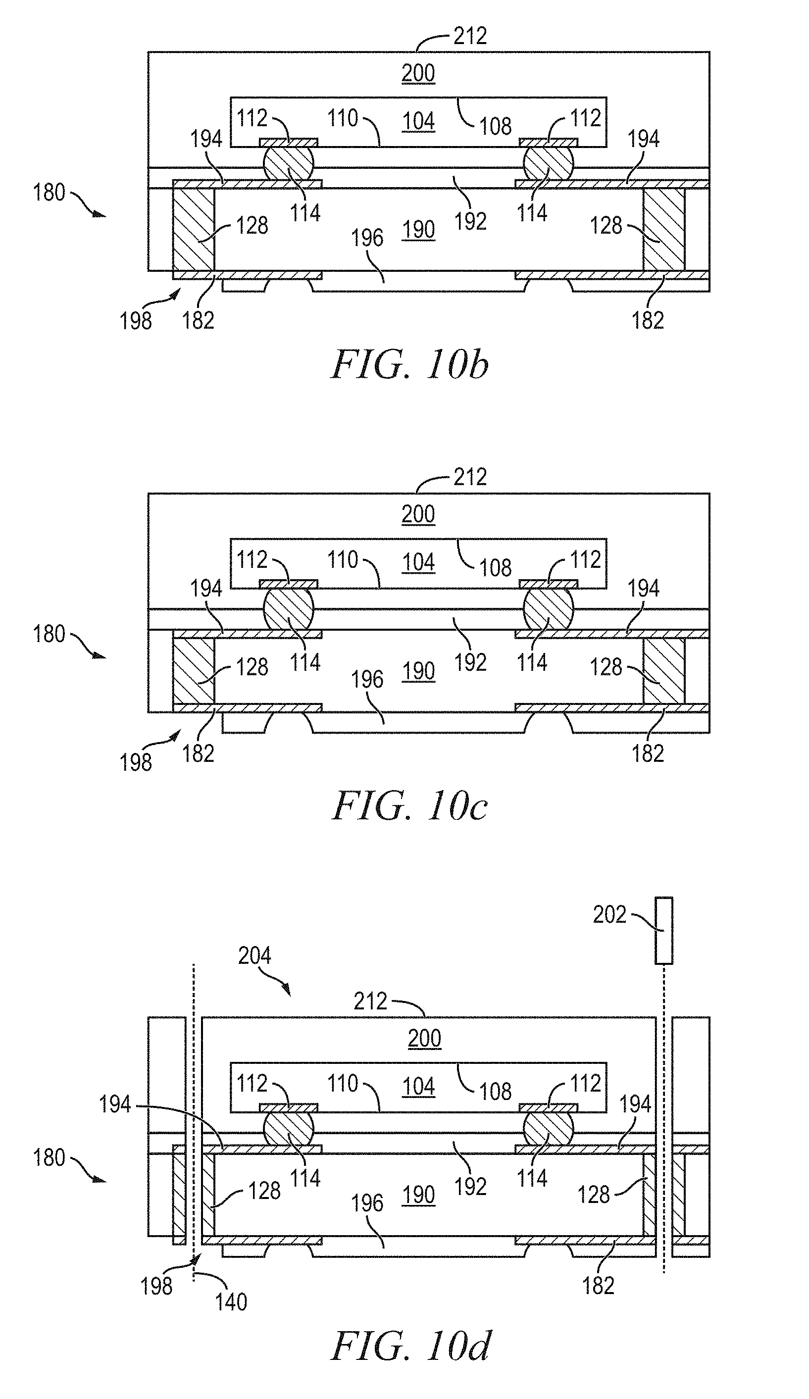
[0051] In another embodiment, substrate panel 180 includes conductive layer 182 formed on a bottom surface of substrate 180 and arranged in a repeating "gear-teeth" pattern completely around die attachment area 184, as shown in FIG. 10a. Die attach area 184 is a bump attach area with solder resist covering and designated for placement of at least one semiconductor die 104. Conductive layer 182a represents one tooth of the gear, conductive layer 182b represents another tooth. One side of conductive layer 182 is continuous along the sides of die attachment area 184. Each tooth of the pattern, e.g. conductive layer 182a, conductive layer 182b, is separated by gap 186. Gaps 186 are regularly spaced between portions of conductive layer 182 to form the gear teeth. One or more conductive vias 128, 135, 146, or 157 can optionally be formed through substrate panel 180 under each portion of conductive layer 182. For example, two conductive vias 128 are formed through substrate panel 180 under conductive layer 182a, and two conductive vias 128 are formed through substrate panel 180 under conductive layer 182b. Substrate panel 180 will be singulated through dicing lines 188. The repeating gear-tooth pattern of conductive layer 182, with optional conductive vias 128, provides enhanced contact surface area along the vertical side surface post singulation.
[0052] In FIG. 10b, semiconductor die 104 from FIG. 1c are positioned over die attach area 184 of substrate panel 180 using a pick and place operation, similar to FIGS. 3a-3b. An encapsulant or molding compound 200 is deposited over semiconductor die 104 and substrate panel 180, similar to FIG. 3d. Conductive layer 182 and conductive vias 128 extend through core substrate 190, similar to FIG. 2a. A conductive layer 194 is formed over a surface of core substrate 190 opposite conductive layer 182. Conductive layer 194 may have the same "gear-tooth" pattern as conductive layer 182. An insulating or passivation layer 192 is formed over core substrate 190 and conductive layer 194. An insulating or passivation layer 196 is formed over core substrate 190 and conductive layer 182. A portion of insulating layers 192 and 196 is removed by LDA, etching, or other suitable process to expose portions of conductive layers 182 and 194, as well as areas 198 proximate to the connection between conductive layer 182 and conductive vias 128. Areas 198 with no insulating layer 196 extend around a perimeter of substrate panel 180 to provide external ground connection.
[0053] FIG. 10c shows an alternate embodiment with conductive layers 182 and 194 embedded within core substrate 190.
[0054] In FIG. 10d, semiconductor panel 180 is singulated through conductive layer 182 and conductive vias 128 along dicing lines 188, see FIG. 10a, using a saw blade or laser cutting tool 202 into individual semiconductor packages 204. The singulation process has variance and tolerances of the cutting path. The repeating gear-tooth pattern of conductive layer 182, with optional conductive vias 128, provides enhanced contact surface area along vertical side surface 156 post singulation. Core substrate 190 is subject to metal burring during singulation. Metal burr can attach to circuits causing electrical short failure. The gear pattern of conductive layer 182 reduces metal burring effects during singulation. Conductive layer 182 can be a thin layer although rigid relative to core substrate 190.
[0055] In FIG. 11, shielding layer 210 is formed over surfaces 212 and 214 of encapsulant 200, using for example a sputtering process. Shielding layer 210 can be one or more layers of Al, Cu, Sn, Ni, Au, Ag, or other suitable conductive material. Alternatively, shielding layer 210 can be carbonyl iron, stainless steel, nickel silver, low-carbon steel, silicon-iron steel, foil, conductive resin, carbon-black, aluminum flake, and other metals and composites capable of reducing the effects of EMI, RFI, and other inter-device interference. Bumps 216 are formed over conductive layer 182. Shielding layer 210 can also be formed in contact with back surface 108 of semiconductor die 104, as described in FIGS. 9a-9b.
[0056] The repeating pattern of conductive layer 182 and conductive vias 128 provides enhanced contact surface area along vertical side surface 156 to shielding layer 210, given variance during cutting along dicing lines 188. In fact, the total contact area between vertical side surfaces 156 and shielding layer 210 remains substantially uniform and constant, independent of singulation location. The enhanced contact surface area along vertical side surface 156 improves adhesion between conductive layer 182 and conductive vias 128 and shielding layer 210, as well as effectiveness of the shielding layer.
[0057] Shielding layer 210 makes contact to an external ground through conductive layer 182 and conductive vias 128 and conductive layer 182 in areas 198. Alternatively, shielding layer 210 can make contact to an external ground through conductive layer 182, conductive vias 128, conductive layer 194, and bumps 216. Semiconductor die 104 makes functional signal contact with external components through conductive layer 182, conductive vias 128, conductive layer 194, and bumps 216.
[0058] In FIG. 12, shielding layer 210 is formed over surfaces 212 and 214 of encapsulant 200, similar to FIG. 11, and extends over conductive layer 196 in area 198 and into the openings in insulating layer 136. Conductive layer 182 is electrically connected to shielding layer 210.
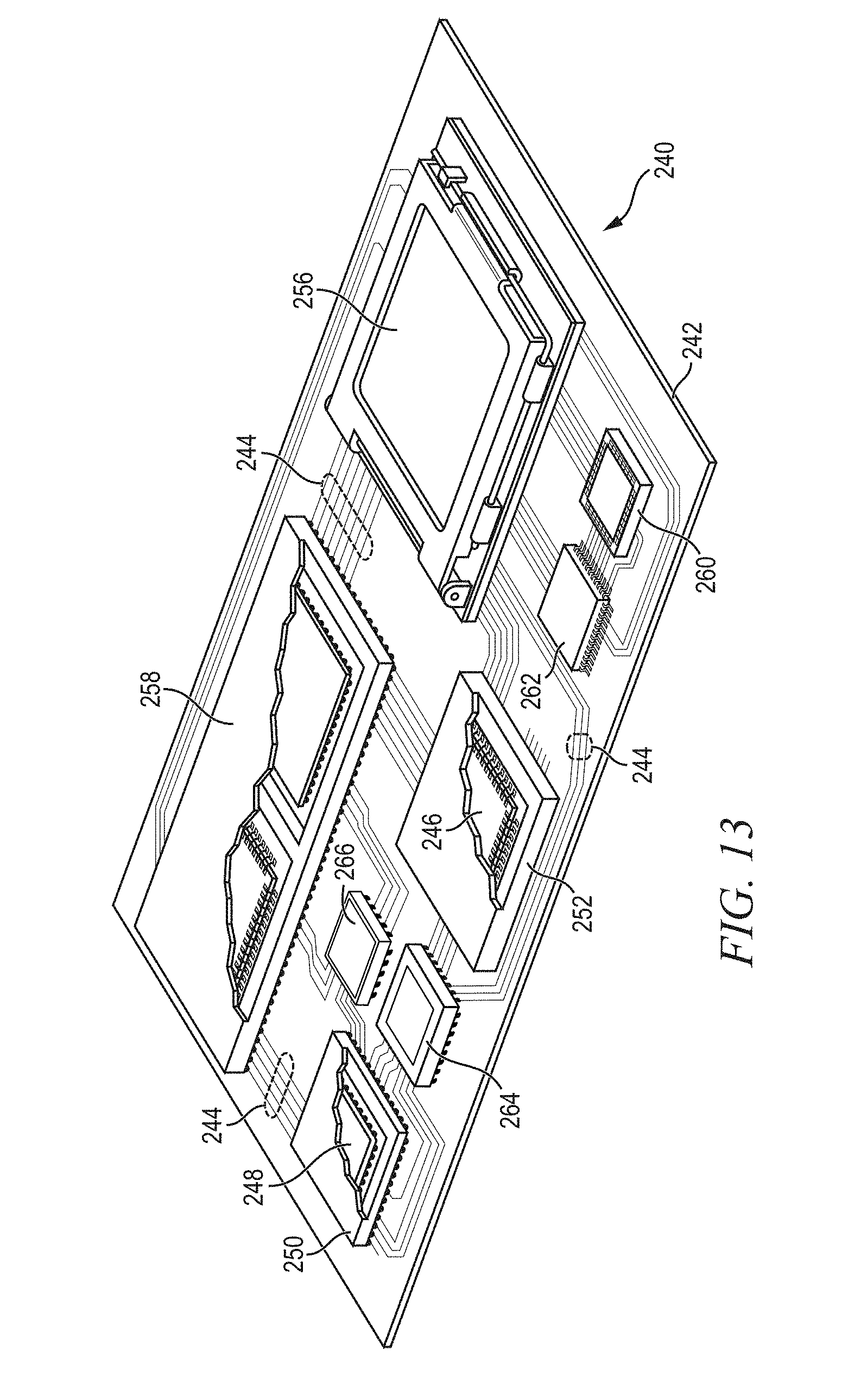
[0059] FIG. 13 illustrates electronic device 240 having a chip carrier substrate or PCB 242 with a plurality of semiconductor packages mounted on a surface of PCB 242, including semiconductor package 154 or 204. Electronic device 240 can have one type of semiconductor package, or multiple types of semiconductor packages, depending on the application.
[0060] Electronic device 240 can be a stand-alone system that uses the semiconductor packages to perform one or more electrical functions. Alternatively, electronic device 240 can be a subcomponent of a larger system. For example, electronic device 240 can be part of a tablet, cellular phone, digital camera, communication system, or other electronic device. Alternatively, electronic device 240 can be a graphics card, network interface card, or other signal processing card that can be inserted into a computer. The semiconductor package can include microprocessors, memories, ASIC, logic circuits, analog circuits, RF circuits, discrete devices, or other semiconductor die or electrical components. Miniaturization and weight reduction are essential for the products to be accepted by the market. The distance between semiconductor devices may be decreased to achieve higher density.
[0061] In FIG. 13, PCB 242 provides a general substrate for structural support and electrical interconnect of the semiconductor packages mounted on the PCB. Conductive signal traces 244 are formed over a surface or within layers of PCB 242 using evaporation, electrolytic plating, electroless plating, screen printing, or other suitable metal deposition process. Signal traces 244 provide for electrical communication between each of the semiconductor packages, mounted components, and other external system components. Traces 244 also provide power and ground connections to each of the semiconductor packages.
[0062] In some embodiments, a semiconductor device has two packaging levels. First level packaging is a technique for mechanically and electrically attaching the semiconductor die to an intermediate substrate. Second level packaging involves mechanically and electrically attaching the intermediate substrate to the PCB. In other embodiments, a semiconductor device may only have the first level packaging where the die is mechanically and electrically mounted directly to the PCB.
[0063] For the purpose of illustration, several types of first level packaging, including bond wire package 246 and flipchip 248, are shown on PCB 242. Additionally, several types of second level packaging, including ball grid array (BGA) 250, bump chip carrier (BCC) 252, land grid array (LGA) 256, multi-chip module (MCM) 258, quad flat non-leaded package (QFN) 260, quad flat package 262, embedded wafer level ball grid array (eWLB) 264, and wafer level chip scale package (WLCSP) 266 are shown mounted on PCB 242. In one embodiment, eWLB 264 is a fan-out wafer level package (Fo-WLP) and WLCSP 266 is a fan-in wafer level package (Fi-WLP). Depending upon the system requirements, any combination of semiconductor packages, configured with any combination of first and second level packaging styles, as well as other electronic components, can be connected to PCB 242. In some embodiments, electronic device 240 includes a single attached semiconductor package, while other embodiments call for multiple interconnected packages. By combining one or more semiconductor packages over a single substrate, manufacturers can incorporate pre-made components into electronic devices and systems. Because the semiconductor packages include sophisticated functionality, electronic devices can be manufactured using less expensive components and a streamlined manufacturing process. The resulting devices are less likely to fail and less expensive to manufacture resulting in a lower cost for consumers.
[0064] While one or more embodiments of the present invention have been illustrated in detail, the skilled artisan will appreciate that modifications and adaptations to those embodiments may be made without departing from the scope of the present invention as set forth in the following claims.
* * * * *
D00000
D00001
D00002
D00003
D00004
D00005
D00006
D00007
D00008
D00009
D00010
D00011
D00012
D00013

D00014
XML
uspto.report is an independent third-party trademark research tool that is not affiliated, endorsed, or sponsored by the United States Patent and Trademark Office (USPTO) or any other governmental organization. The information provided by uspto.report is based on publicly available data at the time of writing and is intended for informational purposes only.
While we strive to provide accurate and up-to-date information, we do not guarantee the accuracy, completeness, reliability, or suitability of the information displayed on this site. The use of this site is at your own risk. Any reliance you place on such information is therefore strictly at your own risk.
All official trademark data, including owner information, should be verified by visiting the official USPTO website at www.uspto.gov. This site is not intended to replace professional legal advice and should not be used as a substitute for consulting with a legal professional who is knowledgeable about trademark law.