Semiconductor Device Including Vertically Integrated Optical And Electronic Devices And Comprising A Superlattice
STEPHENSON; ROBERT JOHN
U.S. patent application number 16/380111 was filed with the patent office on 2019-10-17 for semiconductor device including vertically integrated optical and electronic devices and comprising a superlattice. The applicant listed for this patent is ATOMERA INCORPORATED. Invention is credited to ROBERT JOHN STEPHENSON.
| Application Number | 20190317277 16/380111 |
| Document ID | / |
| Family ID | 66290556 |
| Filed Date | 2019-10-17 |


View All Diagrams
| United States Patent Application | 20190317277 |
| Kind Code | A1 |
| STEPHENSON; ROBERT JOHN | October 17, 2019 |
SEMICONDUCTOR DEVICE INCLUDING VERTICALLY INTEGRATED OPTICAL AND ELECTRONIC DEVICES AND COMPRISING A SUPERLATTICE
Abstract
A semiconductor device may include a substrate having waveguides thereon, and a superlattice overlying the substrate and waveguides. The superlattice may include stacked groups of layers, with each group of layers comprising a stacked base semiconductor monolayers defining a base semiconductor portion, and at least one non-semiconductor monolayer constrained within a crystal lattice of adjacent base semiconductor portions. The semiconductor device may further include an active device layer on the superlattice including at least one active semiconductor device.
| Inventors: | STEPHENSON; ROBERT JOHN; (Duxford, GB) | ||||||||||
| Applicant: |
|
||||||||||
|---|---|---|---|---|---|---|---|---|---|---|---|
| Family ID: | 66290556 | ||||||||||
| Appl. No.: | 16/380111 | ||||||||||
| Filed: | April 10, 2019 |
Related U.S. Patent Documents
| Application Number | Filing Date | Patent Number | ||
|---|---|---|---|---|
| 62656469 | Apr 12, 2018 | |||
| Current U.S. Class: | 1/1 |
| Current CPC Class: | H01L 33/0054 20130101; G02F 2001/01766 20130101; G02B 6/12 20130101; H01L 29/1054 20130101; G02F 1/01708 20130101; G02B 6/12004 20130101; G02B 2006/12061 20130101; H01L 29/152 20130101; H01L 23/5226 20130101; H01L 29/15 20130101; G02B 6/134 20130101; H01L 33/06 20130101; H01L 27/1207 20130101; H01L 27/15 20130101; H01L 33/34 20130101; G02B 2006/12142 20130101; H01L 33/58 20130101; H01L 2933/0058 20130101 |
| International Class: | G02B 6/12 20060101 G02B006/12; H01L 27/12 20060101 H01L027/12; H01L 29/15 20060101 H01L029/15; H01L 23/522 20060101 H01L023/522 |
Claims
1. A semiconductor device comprising: a substrate having a plurality of waveguides thereon; a superlattice overlying the substrate and waveguides, the superlattice comprising a plurality of stacked groups of layers, each group of layers comprising a plurality of stacked base semiconductor monolayers defining a base semiconductor portion, and at least one non-semiconductor monolayer constrained within a crystal lattice of adjacent base semiconductor portions; and an active device layer on the superlattice comprising at least one active semiconductor device.
2. The semiconductor device of claim 1 wherein the substrate comprises a semiconductor-on-insulator (SOI) substrate.
3. The semiconductor device of claim 1 further comprising a plurality of optical modulator regions within the superlattice.
4. The semiconductor device of claim 3 further comprising vias extending through the active device layer to the optical modulator regions.
5. The semiconductor device of claim 3 wherein the optical modulator regions comprise a dopant.
6. The semiconductor device of claim 1 wherein the at least one active optical device comprises at least one metal oxide semiconductor field effect transistor (MOSFET).
7. The semiconductor device of claim 1 wherein the base semiconductor monolayers comprise silicon.
8. The semiconductor device of claim 1 wherein the at least one non-semiconductor monolayer comprises oxygen.
9. A semiconductor device comprising: a semiconductor-on-insulator (SOI) substrate having a plurality of waveguides thereon; a superlattice overlying the SOI substrate and waveguides, the superlattice comprising a plurality of stacked groups of layers, each group of layers comprising a plurality of stacked base semiconductor monolayers defining a base semiconductor portion, and at least one non-semiconductor monolayer constrained within a crystal lattice of adjacent base semiconductor portions; a plurality of optical modulator regions within the superlattice; and an active device layer on the superlattice comprising at least one active semiconductor device.
10. The semiconductor device of claim 9 further comprising vias extending through the active device layer to the optical modulator regions.
11. The semiconductor device of claim 9 wherein the optical modulator regions comprise a dopant.
12. The semiconductor device of claim 9 wherein the at least one active optical device comprises at least one metal oxide semiconductor field effect transistor (MOSFET).
13. The semiconductor device of claim 9 wherein the base semiconductor monolayers comprise silicon.
14. The semiconductor device of claim 9 wherein the at least one non-semiconductor monolayer comprises oxygen.
15. A semiconductor device comprising: a substrate having a plurality of waveguides thereon; a superlattice overlying the substrate and waveguides, the superlattice comprising a plurality of stacked groups of layers, each group of layers comprising a plurality of stacked base silicon monolayers defining a base silicon portion, and at least one oxygen monolayer constrained within a crystal lattice of adjacent base silicon portions; and an active device layer on the superlattice comprising at least one active semiconductor device.
16. The semiconductor device of claim 15 wherein the substrate comprises a semiconductor-on-insulator (SOI) substrate.
17. The semiconductor device of claim 15 further comprising a plurality of optical modulator regions within the superlattice.
18. The semiconductor device of claim 17 further comprising vias extending through the active device layer to the optical modulator regions.
19. The semiconductor device of claim 17 wherein the optical modulator regions comprise a dopant.
20. The semiconductor device of claim 15 wherein the at least one active optical device comprises at least one metal oxide semiconductor field effect transistor (MOSFET).
Description
CROSS-REFERENCE TO RELATED APPLICATIONS
[0001] This application claims the benefit of provisional application Ser. No. 62/656,469 filed Apr. 12, 2018, which is hereby incorporated herein in its entirety by reference.
TECHNICAL FIELD
[0002] The present invention relates to the field of semiconductors, and, more particularly, to optical semiconductor devices and associated methods.
BACKGROUND
[0003] Structures and techniques have been proposed to enhance the performance of semiconductor devices, such as by enhancing the mobility of the charge carriers. For example, U.S. Patent Application No. 2003/0057416 to Currie et al. discloses strained material layers of silicon, silicon-germanium, and relaxed silicon and also including impurity-free zones that would otherwise cause performance degradation. The resulting biaxial strain in the upper silicon layer alters the carrier mobilities enabling higher speed and/or lower power devices. Published U.S. Patent Application No. 2003/0034529 to Fitzgerald et al. discloses a CMOS inverter also based upon similar strained silicon technology.
[0004] U.S. Pat. No. 6,472,685 B2 to Takagi discloses a semiconductor device including a silicon and carbon layer sandwiched between silicon layers so that the conduction band and valence band of the second silicon layer receive a tensile strain. Electrons having a smaller effective mass, and which have been induced by an electric field applied to the gate electrode, are confined in the second silicon layer, thus, an re-channel MOSFET is asserted to have a higher mobility.
[0005] U.S. Pat. No. 4,937,204 to Ishibashi et al. discloses a superlattice in which a plurality of layers, less than eight monolayers, and containing a fractional or binary or a binary compound semiconductor layer, are alternately and epitaxially grown. The direction of main current flow is perpendicular to the layers of the superlattice.
[0006] U.S. Pat. No. 5,357,119 to Wang et al. discloses a Si--Ge short period superlattice with higher mobility achieved by reducing alloy scattering in the superlattice. Along these lines, U.S. Pat. No. 5,683,934 to Candelaria discloses an enhanced mobility MOSFET including a channel layer comprising an alloy of silicon and a second material substitutionally present in the silicon lattice at a percentage that places the channel layer under tensile stress.
[0007] U.S. Pat. No. 5,216,262 to Tsu discloses a quantum well structure comprising two barrier regions and a thin epitaxially grown semiconductor layer sandwiched between the barriers. Each barrier region consists of alternate layers of SiO2/Si with a thickness generally in a range of two to six monolayers. A much thicker section of silicon is sandwiched between the barriers.
[0008] An article entitled "Phenomena in silicon nanostructure devices" also to Tsu and published online Sep. 6, 2000 by Applied Physics and Materials Science & Processing, pp. 391-402 discloses a semiconductor-atomic superlattice (SAS) of silicon and oxygen. The Si/O superlattice is disclosed as useful in a silicon quantum and light-emitting devices. In particular, a green electroluminescence diode structure was constructed and tested. Current flow in the diode structure is vertical, that is, perpendicular to the layers of the SAS. The disclosed SAS may include semiconductor layers separated by adsorbed species such as oxygen atoms, and CO molecules. The silicon growth beyond the adsorbed monolayer of oxygen is described as epitaxial with a fairly low defect density. One SAS structure included a 1.1 nm thick silicon portion that is about eight atomic layers of silicon, and another structure had twice this thickness of silicon. An article to Luo et al. entitled "Chemical Design of Direct-Gap Light-Emitting Silicon" published in Physical Review Letters, Vol. 89, No. 7 (Aug. 12, 2002) further discusses the light emitting SAS structures of Tsu.
[0009] U.S. Pat. No. 6,376,337 to Wang et al. discloses a barrier building block of thin silicon and oxygen, carbon, nitrogen, phosphorous, antimony, arsenic or hydrogen to thereby reduce current flowing vertically through the lattice more than four orders of magnitude. The insulating layer/barrier layer allows for low defect epitaxial silicon to be deposited next to the insulating layer.
[0010] Published Great Britain Patent Application 2,347,520 to Mears et al. discloses that principles of Aperiodic Photonic Band-Gap (APBG) structures may be adapted for electronic bandgap engineering. In particular, the application discloses that material parameters, for example, the location of band minima, effective mass, etc., can be tailored to yield new aperiodic materials with desirable band-structure characteristics. Other parameters, such as electrical conductivity, thermal conductivity and dielectric permittivity or magnetic permeability are disclosed as also possible to be designed into the material.
[0011] Furthermore, U.S. Pat. No. 6,376,337 to Wang et al. discloses a method for producing an insulating or barrier layer for semiconductor devices which includes depositing a layer of silicon and at least one additional element on the silicon substrate whereby the deposited layer is substantially free of defects such that epitaxial silicon substantially free of defects can be deposited on the deposited layer. Alternatively, a monolayer of one or more elements, preferably comprising oxygen, is absorbed on a silicon substrate. A plurality of insulating layers sandwiched between epitaxial silicon forms a barrier composite.
[0012] Despite the existence of such approaches, further enhancements may be desirable for using advanced semiconductor processing techniques in certain applications, including those involving optical devices. An approach for making an integrated circuit including optical components is disclosed in U.S. Pat. No. 7,109,052 to Mears et al., which is assigned to the present Applicant and hereby incorporated herein in its entirety. This approach includes forming at least one active optical device and a waveguide coupled thereto. The waveguide may include a superlattice including a plurality of stacked groups of layers. Each group of layers of the superlattice may include a plurality of stacked base semiconductor monolayers defining a base semiconductor portion and an energy band-modifying layer thereon. The energy-band modifying layer may include at least one non-semiconductor monolayer constrained within a crystal lattice of adjacent base semiconductor portions.
SUMMARY
[0013] A semiconductor device may include a substrate having a plurality of waveguides thereon, and a superlattice overlying the substrate and waveguides. The superlattice may include a plurality of stacked groups of layers, with each group of layers comprising a plurality of stacked base semiconductor monolayers defining a base semiconductor portion, and at least one non-semiconductor monolayer constrained within a crystal lattice of adjacent base semiconductor portions. The semiconductor device may further include an active device layer on the superlattice including at least one active semiconductor device.
[0014] By way of example, the substrate may comprise a semiconductor-on-insulator (SOI) substrate. The semiconductor device may further include a plurality of optical modulator regions within the superlattice, as well as vias extending through the active device layer to the optical modulator regions. Furthermore, the optical modulator regions may comprise a dopant.
[0015] In an example embodiment, the at least one active optical device may comprise at least one metal oxide semiconductor field effect transistor (MOSFET). By way of example, the base semiconductor monolayers may comprise silicon, and the at least one non-semiconductor monolayer may comprise oxygen.
BRIEF DESCRIPTION OF THE DRAWINGS
[0016] FIG. 1 is a greatly enlarged schematic cross-sectional view of a superlattice for use in a semiconductor device in accordance with the present invention.
[0017] FIG. 2 is a perspective schematic atomic diagram of a portion of the superlattice shown in FIG. 1.
[0018] FIG. 3 is a greatly enlarged schematic cross-sectional view of another embodiment of a superlattice in accordance with the invention.
[0019] FIG. 4A is a graph of the calculated band structure from the gamma point (G) for both bulk silicon as in the prior art, and for the 4/1 Si/O superlattice as shown in FIGS. 1-2.
[0020] FIG. 4B is a graph of the calculated band structure from the Z point for both bulk silicon as in the prior art, and for the 4/1 Si/O superlattice as shown in FIGS. 1-2.
[0021] FIG. 4C is a graph of the calculated band structure from both the gamma and Z points for both bulk silicon as in the prior art, and for the 5/1/3/1 Si/O superlattice as shown in FIG. 3.
[0022] FIG. 5 is a schematic cross-sectional diagram of a MOSFET stacked on an optical device and including a superlattice in accordance with an example embodiment.
[0023] FIGS. 6A-6E are a series of a schematic cross-sectional diagrams illustrating a method of fabricating the device of FIG. 5.
DETAILED DESCRIPTION OF THE PREFERRED EMBODIMENTS
[0024] Example embodiments will now be described more fully hereinafter with reference to the accompanying drawings, in which the example embodiments are shown. The embodiments may, however, be implemented in many different forms and should not be construed as limited to the specific examples set forth herein. Rather, these embodiments are provided so that this disclosure will be thorough and complete. Like numbers refer to like elements throughout, and prime notation is used to indicate similar elements in different embodiments.
[0025] Generally speaking, the present disclosure relates to the formation of enhanced structures in planar and vertical semiconductor devices through the use of an enhanced semiconductor superlattice. The enhanced semiconductor superlattice is also referred to as an "MST" layer or "MST technology" in this disclosure.
[0026] More particularly, the MST technology relates to advanced semiconductor materials such as the superlattice 25 described further below. Applicant theorizes, without wishing to be bound thereto, that certain superlattices as described herein reduce the effective mass of charge carriers and that this thereby leads to higher charge carrier mobility. Effective mass is described with various definitions in the literature. As a measure of the improvement in effective mass Applicant's use a "conductivity reciprocal effective mass tensor", M.sub.e.sup.-1 and M.sub.h.sup.-1 for electrons and holes respectively, defined as:
M e , ij - 1 ( E F , T ) = E > E F .intg. B . Z . ( .gradient. k E ( k , n ) ) i ( .gradient. k E ( k , n ) ) j .differential. f ( E ( k , n ) , E F , T ) .differential. E d 3 k E > E F .intg. B . Z . f ( E ( k , n ) , E F , T ) d 3 k ##EQU00001##
for electrons and:
M h , ij - 1 ( E F , T ) = - E > E F .intg. B . Z . ( .gradient. k E ( k , n ) ) i ( .gradient. k E ( k , n ) ) j .differential. f ( E ( k , n ) , E F , T ) .differential. E d 3 k E > E F .intg. B . Z . ( 1 - f ( E ( k , n ) , E F , T ) ) d 3 k ##EQU00002##
for holes, where f is the Fermi-Dirac distribution, E.sub.F is the Fermi energy, T is the temperature, E(k,n) is the energy of an electron in the state corresponding to wave vector k and the n.sup.th energy band, the indices i and j refer to Cartesian coordinates x, y and z, the integrals are taken over the Brillouin zone (B.Z.), and the summations are taken over bands with energies above and below the Fermi energy for electrons and holes respectively.
[0027] Applicant's definition of the conductivity reciprocal effective mass tensor is such that a tensorial component of the conductivity of the material is greater for greater values of the corresponding component of the conductivity reciprocal effective mass tensor. Again, Applicant theorizes without wishing to be bound thereto that the superlattices described herein set the values of the conductivity reciprocal effective mass tensor so as to enhance the conductive properties of the material, such as typically for a preferred direction of charge carrier transport. The inverse of the appropriate tensor element is referred to as the conductivity effective mass. In other words, to characterize semiconductor material structures, the conductivity effective mass for electrons/holes as described above and calculated in the direction of intended carrier transport is used to distinguish improved materials.
[0028] Applicant has identified improved materials or structures for use in semiconductor devices. More specifically, Applicant has identified materials or structures having energy band structures for which the appropriate conductivity effective masses for electrons and/or holes are substantially less than the corresponding values for silicon. In addition to the enhanced mobility characteristics of these structures, they may also be formed or used in such a manner that they provide piezoelectric, pyroelectric, and/or ferroelectric properties that are advantageous for use in a variety of different types of devices, as will be discussed further below.
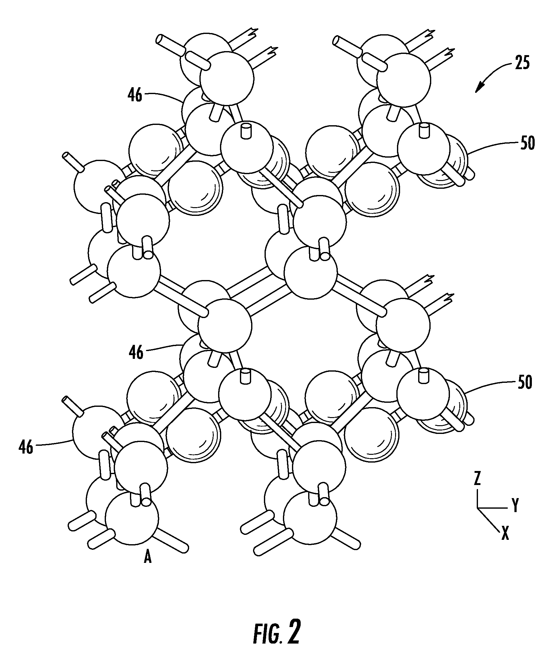
[0029] Referring now to FIGS. 1 and 2, the materials or structures are in the form of a superlattice 25 whose structure is controlled at the atomic or molecular level and may be formed using known techniques of atomic or molecular layer deposition. The superlattice 25 includes a plurality of layer groups 45a-45n arranged in stacked relation, as perhaps best understood with specific reference to the schematic cross-sectional view of FIG. 1.
[0030] Each group of layers 45a-45n of the superlattice 25 illustratively includes a plurality of stacked base semiconductor monolayers 46 defining a respective base semiconductor portion 46a-46n and an energy band-modifying layer 50 thereon. The energy band-modifying layers 50 are indicated by stippling in FIG. 1 for clarity of illustration.
[0031] The energy band-modifying layer 50 illustratively includes one non-semiconductor monolayer constrained within a crystal lattice of adjacent base semiconductor portions. By "constrained within a crystal lattice of adjacent base semiconductor portions" it is meant that at least some semiconductor atoms from opposing base semiconductor portions 46a-46n are chemically bound together through the non-semiconductor monolayer 50 therebetween, as seen in FIG. 2. Generally speaking, this configuration is made possible by controlling the amount of non-semiconductor material that is deposited on semiconductor portions 46a-46n through atomic layer deposition techniques so that not all (i.e., less than full or 100% coverage) of the available semiconductor bonding sites are populated with bonds to non-semiconductor atoms, as will be discussed further below. Thus, as further monolayers 46 of semiconductor material are deposited on or over a non-semiconductor monolayer 50, the newly deposited semiconductor atoms will populate the remaining vacant bonding sites of the semiconductor atoms below the non-semiconductor monolayer.
[0032] In other embodiments, more than one such non-semiconductor monolayer may be possible. It should be noted that reference herein to a non-semiconductor or semiconductor monolayer means that the material used for the monolayer would be a non-semiconductor or semiconductor if formed in bulk. That is, a single monolayer of a material, such as silicon, may not necessarily exhibit the same properties that it would if formed in bulk or in a relatively thick layer, as will be appreciated by those skilled in the art.
[0033] Applicant theorizes without wishing to be bound thereto that energy band-modifying layers 50 and adjacent base semiconductor portions 46a-46n cause the superlattice 25 to have a lower appropriate conductivity effective mass for the charge carriers in the parallel layer direction than would otherwise be present. Considered another way, this parallel direction is orthogonal to the stacking direction. The band modifying layers 50 may also cause the superlattice 25 to have a common energy band structure, while also advantageously functioning as an insulator between layers or regions vertically above and below the superlattice.
[0034] Moreover, this superlattice structure may also advantageously act as a barrier to dopant and/or material diffusion between layers vertically above and below the superlattice 25. These properties may thus advantageously allow the superlattice 25 to provide an interface for high-K dielectrics which not only reduces diffusion of the high-K material into the channel region, but which may also advantageously reduce unwanted scattering effects and improve device mobility, as will be appreciated by those skilled in the art.
[0035] It is also theorized that semiconductor devices including the superlattice 25 may enjoy a higher charge carrier mobility based upon the lower conductivity effective mass than would otherwise be present. In some embodiments, and as a result of the band engineering achieved by the present invention, the superlattice 25 may further have a substantially direct energy bandgap that may be particularly advantageous for optoelectronic devices, for example.
[0036] The superlattice 25 also illustratively includes a cap layer 52 on an upper layer group 45n. The cap layer 52 may comprise a plurality of base semiconductor monolayers 46. The cap layer 52 may have between 2 to 100 monolayers of the base semiconductor, and, more preferably between 10 to 50 monolayers.
[0037] Each base semiconductor portion 46a-46n may comprise a base semiconductor selected from the group consisting of Group IV semiconductors, Group III-V semiconductors, and Group II-VI semiconductors. Of course, the term Group IV semiconductors also includes Group IV-IV semiconductors, as will be appreciated by those skilled in the art. More particularly, the base semiconductor may comprise at least one of silicon and germanium, for example.
[0038] Each energy band-modifying layer 50 may comprise a non-semiconductor selected from the group consisting of oxygen, nitrogen, fluorine, carbon and carbon-oxygen, for example. The non-semiconductor is also desirably thermally stable through deposition of a next layer to thereby facilitate manufacturing. In other embodiments, the non-semiconductor may be another inorganic or organic element or compound that is compatible with the given semiconductor processing as will be appreciated by those skilled in the art. More particularly, the base semiconductor may comprise at least one of silicon and germanium, for example
[0039] It should be noted that the term monolayer is meant to include a single atomic layer and also a single molecular layer. It is also noted that the energy band-modifying layer 50 provided by a single monolayer is also meant to include a monolayer wherein not all of the possible sites are occupied (i.e., there is less than full or 100% coverage). For example, with particular reference to the atomic diagram of FIG. 2, a 4/1 repeating structure is illustrated for silicon as the base semiconductor material, and oxygen as the energy band-modifying material. Only half of the possible sites for oxygen are occupied in the illustrated example.
[0040] In other embodiments and/or with different materials this one-half occupation would not necessarily be the case as will be appreciated by those skilled in the art. Indeed, it can be seen even in this schematic diagram, that individual atoms of oxygen in a given monolayer are not precisely aligned along a flat plane as will also be appreciated by those of skill in the art of atomic deposition. By way of example, a preferred occupation range is from about one-eighth to one-half of the possible oxygen sites being full, although other numbers may be used in certain embodiments.
[0041] Silicon and oxygen are currently widely used in conventional semiconductor processing, and, hence, manufacturers will be readily able to use these materials as described herein. Atomic or monolayer deposition is also now widely used. Accordingly, semiconductor devices incorporating the superlattice 25 may be readily adopted and implemented, as will be appreciated by those skilled in the art.
[0042] It is theorized without Applicant wishing to be bound thereto that for a superlattice, such as the Si/O superlattice, for example, that the number of silicon monolayers should desirably be seven or less so that the energy band of the superlattice is common or relatively uniform throughout to achieve the desired advantages. The 4/1 repeating structure shown in FIGS. 1 and 2, for Si/O has been modeled to indicate an enhanced mobility for electrons and holes in the X direction. For example, the calculated conductivity effective mass for electrons (isotropic for bulk silicon) is 0.26 and for the 4/1 SiO superlattice in the X direction it is 0.12 resulting in a ratio of 0.46. Similarly, the calculation for holes yields values of 0.36 for bulk silicon and 0.16 for the 4/1 Si/O superlattice resulting in a ratio of 0.44.
[0043] While such a directionally preferential feature may be desired in certain semiconductor devices, other devices may benefit from a more uniform increase in mobility in any direction parallel to the groups of layers. It may also be beneficial to have an increased mobility for both electrons and holes, or just one of these types of charge carriers as will be appreciated by those skilled in the art.
[0044] The lower conductivity effective mass for the 4/1 Si/O embodiment of the superlattice 25 may be less than two-thirds the conductivity effective mass than would otherwise occur, and this applies for both electrons and holes. Of course, the superlattice 25 may further comprise at least one type of conductivity dopant therein, as will also be appreciated by those skilled in the art.
[0045] Indeed, referring now additionally to FIG. 3, another embodiment of a superlattice 25' in accordance with the invention having different properties is now described. In this embodiment, a repeating pattern of 3/1/5/1 is illustrated. More particularly, the lowest base semiconductor portion 46a' has three monolayers, and the second lowest base semiconductor portion 46b' has five monolayers. This pattern repeats throughout the superlattice 25'. The energy band-modifying layers 50' may each include a single monolayer. For such a superlattice 25' including Si/O, the enhancement of charge carrier mobility is independent of orientation in the plane of the layers. Those other elements of FIG. 3 not specifically mentioned are similar to those discussed above with reference to FIG. 1 and need no further discussion herein.
[0046] In some device embodiments, all of the base semiconductor portions of a superlattice may be a same number of monolayers thick. In other embodiments, at least some of the base semiconductor portions may be a different number of monolayers thick. In still other embodiments, all of the base semiconductor portions may be a different number of monolayers thick.
[0047] In FIGS. 4A-4C, band structures calculated using Density Functional Theory (DFT) are presented. It is well known in the art that DFT underestimates the absolute value of the bandgap. Hence all bands above the gap may be shifted by an appropriate "scissors correction." However, the shape of the band is known to be much more reliable. The vertical energy axes should be interpreted in this light.
[0048] FIG. 4A shows the calculated band structure from the gamma point (G) for both bulk silicon (represented by continuous lines) and for the 4/1 Si/O superlattice 25 shown in FIG. 1 (represented by dotted lines). The directions refer to the unit cell of the 4/1 Si/O structure and not to the conventional unit cell of Si, although the (001) direction in the figure does correspond to the (001) direction of the conventional unit cell of Si, and, hence, shows the expected location of the Si conduction band minimum. The (100) and (010) directions in the figure correspond to the (110) and (-110) directions of the conventional Si unit cell. Those skilled in the art will appreciate that the bands of Si on the figure are folded to represent them on the appropriate reciprocal lattice directions for the 4/1 Si/O structure.
[0049] It can be seen that the conduction band minimum for the 4/1 Si/O structure is located at the gamma point in contrast to bulk silicon (Si), whereas the valence band minimum occurs at the edge of the Brillouin zone in the (001) direction which we refer to as the Z point. One may also note the greater curvature of the conduction band minimum for the 4/1 Si/O structure compared to the curvature of the conduction band minimum for Si owing to the band splitting due to the perturbation introduced by the additional oxygen layer.
[0050] FIG. 4B shows the calculated band structure from the Z point for both bulk silicon (continuous lines) and for the 4/1 Si/O superlattice 25 (dotted lines). This figure illustrates the enhanced curvature of the valence band in the (100) direction.
[0051] FIG. 4C shows the calculated band structure from both the gamma and Z point for both bulk silicon (continuous lines) and for the 5/1/3/1 Si/O structure of the superlattice 25' of FIG. 3 (dotted lines). Due to the symmetry of the 5/1/3/1 Si/O structure, the calculated band structures in the (100) and (010) directions are equivalent. Thus, the conductivity effective mass and mobility are expected to be isotropic in the plane parallel to the layers, i.e. perpendicular to the (001) stacking direction. Note that in the 5/1/3/1 Si/O example the conduction band minimum and the valence band maximum are both at or close to the Z point.
[0052] Although increased curvature is an indication of reduced effective mass, the appropriate comparison and discrimination may be made via the conductivity reciprocal effective mass tensor calculation. This leads Applicant to further theorize that the 5/1/3/1 superlattice 25' should be substantially direct bandgap. As will be understood by those skilled in the art, the appropriate matrix element for optical transition is another indicator of the distinction between direct and indirect bandgap behavior.
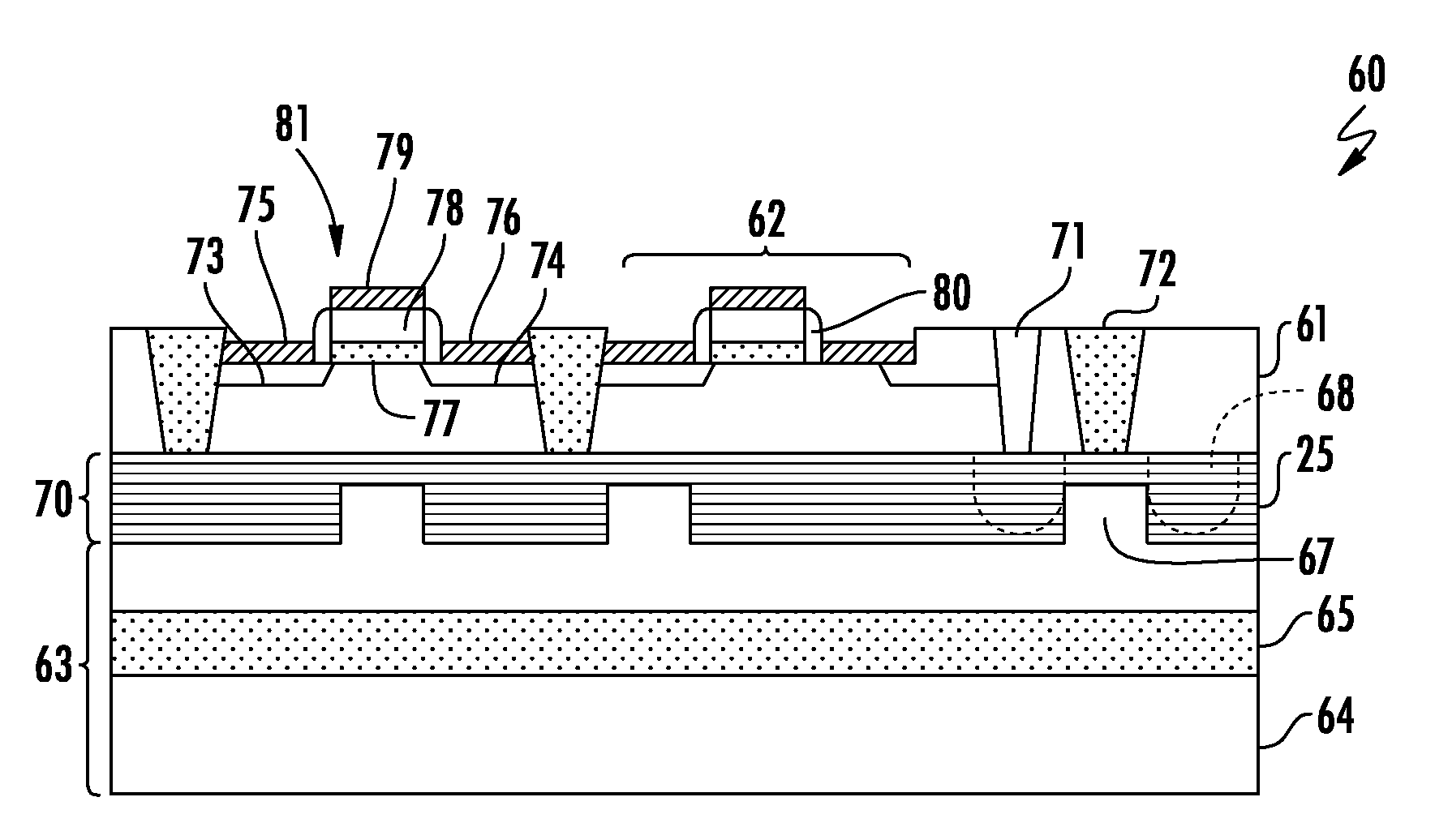
[0053] Using the above-described measures, one can select materials having improved band structures for specific purposes. Turning now to FIG. 5, one such example would be a superlattice 25 material in a 3D photonic/electronic semiconductor device 60. By way of background, the silicon surface area in Ultra Large Scale Integration (ULSI) chips is typically expensive, and thus methods have been sought to increase the device density on wafers. Additionally, photonic components are, in general, large devices compared to cutting edge Integrated Circuits (ICs) with interaction lengths measured on a millimeter length scale. The ability to vertically stack photonic and IC devices on a single chip is one method to reduce cost and increase the functionality per area on a chip.
[0054] Oxygen in silicon (SIMOX) techniques have been implemented for stacking MOSFET devices on top of optical waveguides. See, e.g., Appl. Phys. Lett 88, 121108 (2006). The SIMOX process, however, results in a large concentration of defects which contribute to the degradation of device properties of the MOSFETs. Significantly, the source-drain leakage current is non-zero for sub-threshold gate voltages.
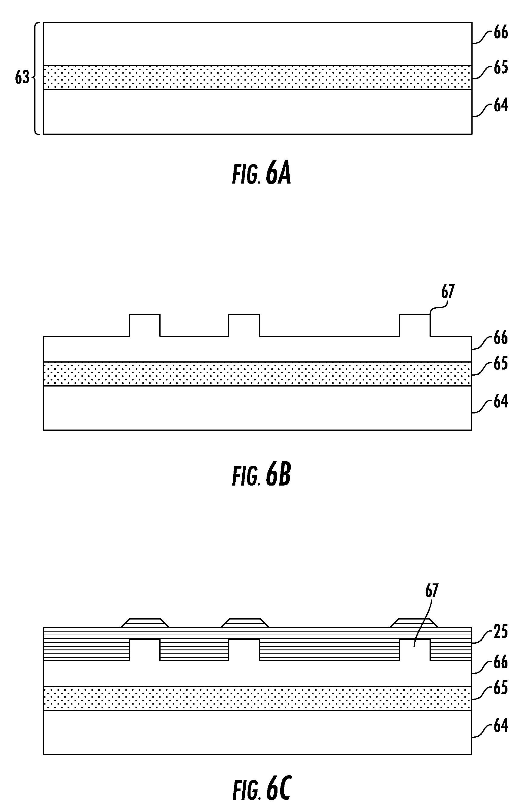
[0055] In the illustrated example, the superlattice material 25 is advantageously used as a low index of refraction material for confining an optical waveguide, in addition to creating a high quality epitaxial silicon active device layer 61 which may accordingly result in high quality MOSFET devices 62 stacked on top of the optical waveguide and/or optical devices. Referring additionally to FIGS. 6A-6E, a method for fabricating the device 60, which illustratively includes a buried optical device layer or chip 70 (in which waveguides, splitters, optical transmitters/receivers, etc., may be defined) on an SOI wafer or substrate 63 via standard patterning and etching processes is now described.
[0056] The SOI substrate 63 illustratively includes a bottom semiconductor (e.g., silicon) layer 64, an insulating layer 65 (e.g., SiO.sub.2) on the bottom semiconductor layer, and an upper semiconductor (e.g., silicon) layer 66 on the insulating layer. After etching waveguides/waveguide grooves 67 into the semiconductor layer 66 on the SOI wafer 63 (FIGS. 6A-6B), a relatively thick superlattice film 25 is grown on the upper semiconductor layer (FIG. 6C), followed by implantation of optical modulator regions 68, etc., and chemical-mechanical polishing/planarization (CMP) (FIG. 6D). It should be noted that the implantation step may optionally be performed at a later time in some embodiments, if desired.
[0057] An epitaxial semiconductor (e.g., silicon) layer 61 is then grown (FIG. 6E) for covering the optical device layer 70 and to provide an active device layer for subsequent CMOS processing to form ICs (here the MOSFETs 62), contact vias, etc., above the buried optical chip, as will be appreciated by those skilled in the art. Thereafter, deep electrically conductive vias 71 may be etched for providing contacts to optical modulators 67, etc., for example, within the optical device layer 70. In the illustrated example, isolation regions 72 (e.g., shallow trench isolation (STI) oxide regions) separate the electrical devices (here the MOSFETs 62) within the active device layer 61. Moreover, each MOSFET 62 illustratively includes source and drain regions 73, 74 with respective metal/silicide contacts 75, 76, and a gate 75 which illustratively includes a gate insulator 77, gate electrode 78, and metal/silicide contact 79, and sidewall spacers 80. However, it should be noted that other FET configurations and other electrical/electronic devices may be used in different embodiments.
[0058] In some embodiments, a superlattice layer 25 may also advantageously be used to produce the underlying low index region, thereby avoiding the need for the SOI substrate 63 and instead allowing a standard semiconductor (e.g., silicon) substrate with a first superlattice layer to be used as the optical isolation region, as will be appreciated by those skilled in the art. The implementation of the superlattice layer 25 for stacking devices may advantageously result in an uppermost layer of silicon of much better quality than the one produced by existing techniques (e.g., SIMOX). This will result in high quality MOSFET (or other) devices stacked on optical devices, as opposed to existing techniques which may lead to a relatively low quality uppermost silicon layer and, consequently, a relatively low quality MOSFET device stacked on top of optical devices.
[0059] Many modifications and other embodiments will come to the mind of one skilled in the art having the benefit of the teachings presented in the foregoing descriptions and the associated drawings. Therefore, it is understood that the foregoing is not to be limited to the example embodiments, and that modifications and other embodiments are intended to be included within the scope of the appended claims.
* * * * *
D00000
D00001
D00002
D00003
D00004
D00005
D00006
D00007
D00008
D00009
XML
uspto.report is an independent third-party trademark research tool that is not affiliated, endorsed, or sponsored by the United States Patent and Trademark Office (USPTO) or any other governmental organization. The information provided by uspto.report is based on publicly available data at the time of writing and is intended for informational purposes only.
While we strive to provide accurate and up-to-date information, we do not guarantee the accuracy, completeness, reliability, or suitability of the information displayed on this site. The use of this site is at your own risk. Any reliance you place on such information is therefore strictly at your own risk.
All official trademark data, including owner information, should be verified by visiting the official USPTO website at www.uspto.gov. This site is not intended to replace professional legal advice and should not be used as a substitute for consulting with a legal professional who is knowledgeable about trademark law.