Bulk Cmos Devices With Enhanced Performance And Methods Of Forming The Same Utilizing Bulk Cmos Process
Costa; Julio C. ; et al.
U.S. patent application number 16/368210 was filed with the patent office on 2019-10-03 for bulk cmos devices with enhanced performance and methods of forming the same utilizing bulk cmos process. The applicant listed for this patent is Qorvo US, Inc.. Invention is credited to Michael Carroll, Julio C. Costa, Dirk Robert Walter Leipold, George Maxim, Baker Scott.
| Application Number | 20190304977 16/368210 |
| Document ID | / |
| Family ID | 68055483 |
| Filed Date | 2019-10-03 |


View All Diagrams
| United States Patent Application | 20190304977 |
| Kind Code | A1 |
| Costa; Julio C. ; et al. | October 3, 2019 |
BULK CMOS DEVICES WITH ENHANCED PERFORMANCE AND METHODS OF FORMING THE SAME UTILIZING BULK CMOS PROCESS
Abstract
The present disclosure relates to a bulk complementary-metal-oxide-semiconductor (CMOS) device including a device substrate, a thinned device die with a device region over the device substrate, a first mold compound, and a second mold compound. The device region includes a back-end-of-line (BEOL) portion and a front-end-of-line (FEOL) portion over the BEOL portion. The first mold compound resides over the device substrate, surrounds the thinned device die, and extends vertically beyond the thinned device die to define an opening over the thinned device die and within the first mold compound. The second mold compound fills the opening and directly connects the thinned device die. Herein, a silicon material with a resistivity between 5 Ohm-cm and 30000 Ohm-cm does not exist between the second mold compound and the thinned device die.
| Inventors: | Costa; Julio C.; (Oak Ridge, NC) ; Carroll; Michael; (Jamestown, NC) ; Leipold; Dirk Robert Walter; (San Jose, CA) ; Maxim; George; (Saratoga, CA) ; Scott; Baker; (San Jose, CA) | ||||||||||
| Applicant: |
|
||||||||||
|---|---|---|---|---|---|---|---|---|---|---|---|
| Family ID: | 68055483 | ||||||||||
| Appl. No.: | 16/368210 | ||||||||||
| Filed: | March 28, 2019 |
Related U.S. Patent Documents
| Application Number | Filing Date | Patent Number | ||
|---|---|---|---|---|
| 62649351 | Mar 28, 2018 | |||
| Current U.S. Class: | 1/1 |
| Current CPC Class: | H01L 24/20 20130101; H01L 24/24 20130101; H01L 2224/24137 20130101; H01L 21/30604 20130101; H01L 24/17 20130101; H01L 29/16 20130101; H01L 23/3121 20130101; H01L 27/0928 20130101; H01L 24/19 20130101; H01L 24/16 20130101; H01L 29/0696 20130101; H01L 29/78 20130101; H01L 2224/13101 20130101; H01L 23/3135 20130101; H01L 24/13 20130101; H01L 2224/73253 20130101; H01L 2224/16225 20130101; H01L 23/5226 20130101; H01L 21/823871 20130101; H01L 24/82 20130101; H01L 21/02381 20130101; H01L 21/823892 20130101; H01L 21/56 20130101; H01L 2224/13147 20130101; H01L 21/565 20130101; H01L 27/092 20130101; H01L 2924/181 20130101; H01L 2224/13101 20130101; H01L 2924/014 20130101; H01L 2924/00014 20130101; H01L 2224/13147 20130101; H01L 2924/00014 20130101; H01L 2924/181 20130101; H01L 2924/00012 20130101 |
| International Class: | H01L 27/092 20060101 H01L027/092; H01L 23/00 20060101 H01L023/00; H01L 23/522 20060101 H01L023/522; H01L 23/31 20060101 H01L023/31; H01L 21/56 20060101 H01L021/56; H01L 21/306 20060101 H01L021/306; H01L 21/02 20060101 H01L021/02; H01L 21/8238 20060101 H01L021/8238; H01L 29/16 20060101 H01L029/16; H01L 29/06 20060101 H01L029/06 |
Claims
1. An apparatus comprising: a device substrate having a top surface; a thinned device die comprising a device region and a plurality of bump structures, wherein: the device region comprises a back-end-of-line (BEOL) portion with a plurality of connecting layers and a front-end-of-line (FEOL) portion residing over the BEOL portion, wherein the FEOL portion comprises a contact layer and an active layer that resides over the contact layer and has a first component cell; and the plurality of bump structures are formed at a bottom surface of the BEOL portion and attached to the top surface of the device substrate, wherein the plurality of bump structures are electrically coupled to the FEOL portion via certain ones of the plurality of connecting layers; a first mold compound residing over the top surface of the device substrate, surrounding the thinned device die, and extending vertically beyond the thinned device die to define an opening over the thinned device die and within the first mold compound, wherein a top surface of the thinned device is at the bottom of the opening; and a second mold compound substantially filling the opening and in contact with the top surface of the thinned device, wherein a silicon material, which has a resistivity between 5 Ohm-cm and 30000 Ohm-cm, does not exist between the second mold compound and the active layer of the thinned device.
2. The apparatus of claim 1 wherein the active layer further includes isolation sections surrounding the first component cell.
3. The apparatus of claim 2 wherein: the first component cell is configured to provide an N-type field-effect transistor (NFET), wherein the first component includes a P-well with an N-source and an N-drain inside, and an N-well encapsulating the P-well and surrounded by the isolation sections; the N-well is doped with an N-dopant having a density more than 1E15 cm-3; and the active layer further includes a P-type passive section over both the first component cell and the isolation sections.
4. The apparatus of claim 2 wherein: the first component cell is configured to provide a P-type field-effect transistor (PFET) and includes an N-well with a P-source and a P-drain, wherein the N-well is surrounded by the isolation sections; the N-well is doped with an N-dopant having a density between 1E14 cm-3 and 1E19 cm-3; and the active layer further includes a P-type passive section over both the first component cell and the isolation sections.
5. The apparatus of claim 1 wherein the active layer further includes a second component cell and isolation sections that separate the first component cell from the second component cell.
6. The apparatus of claim 5 wherein the first component cell and the second component cell are electrically coupled by one of the plurality of connecting layers within the BEOL portion.
7. The apparatus of claim 6 wherein: the first component cell is configured to provide a first NFET, wherein the first component cell includes a first P-well with a first N-source and a first N-drain inside, and a first N-well encapsulating the first P-well; the second component cell is configured to provide a second NFET, wherein the second component cell includes a second P-well with a second N-source and a second N-drain inside, and a second N-well encapsulating the second P-well; the first N-well and the second N-well are doped with an N-dopant having a density more than 1E15 cm-3; the isolation sections reside between first N-well of the first component cell and the second N-well of the second component cell; the first N-source of the first component cell is electrically coupled to the second N-drain of the second component cell by one of the plurality of connecting layers within the BEOL portion; and the active layer further includes a P-type passive section over the first component cell, the second component cell, and the isolation sections.
8. The apparatus of claim 1 wherein the thinned device die further comprises an interfacial layer directly over the active layer and within the opening, wherein: the interfacial layer is formed of silicon germanium (SiGe), or silicon with a boron dopant having a density greater than 1E16 cm-3; a top surface of the interfacial layer is the top surface of the thinned device die; and the second mold compound is in contact with the interfacial layer.
9. The apparatus of claim 1 wherein a top surface of the active layer is the top surface of the thinned device die, such that the second mold compound is in contact with the top surface of the active layer.
10. The apparatus of claim 1 wherein the second mold compound has a thermal conductivity greater than 1 W/mK.
11. The apparatus of claim 1 wherein the second mold compound has a dielectric constant less than 8.
12. The apparatus of claim 11 wherein the first mold compound and the second mold compound have a dielectric constant between 3 and 5.
13. A method comprising: providing a precursor package having a device substrate, a first mold compound, and a device die with a device region, an interfacial layer, a bulk silicon handle substrate, and a plurality of bump structures, wherein: the device region comprises a back-end-of-line (BEOL) portion with a plurality of connecting layers and a front-end-of-line (FEOL) portion residing over the BEOL portion; the FEOL portion comprises a contact layer and an active layer that resides over the contact layer and has a first component cell; the plurality of bump structures are formed at a bottom surface of the BEOL portion and attached to the device substrate, wherein the plurality of bump structures are electrically coupled to the FEOL portion via certain ones of the plurality of connecting layers; the interfacial layer resides over the active layer and is formed of SiGe, or silicon with a boron dopant having a density greater than 1E16 cm-3; the bulk silicon handle substrate resides over the interfacial layer; and the first mold compound resides over the device substrate to encapsulate the device die; thinning down the first mold compound to expose the bulk silicon handle substrate; removing the bulk silicon handle substrate completely to provide a thinned device die and form an opening within the first mold compound and over the thinned device die; and applying a second mold compound to substantially fill the opening and reside directly over the thinned device die.
14. The method of claim 13 wherein the second mold compound is in contact with the interfacial layer after the second mold compound is applied.
15. The method of claim 13 further comprising removing the interfacial layer before applying the second mold compound, wherein the active layer is in contact with the second mold compound after the second mold compound is applied.
16. The method of claim 13 wherein providing the precursor package comprises: providing an initial wafer that includes a silicon epitaxial layer, the interfacial layer over the silicon epitaxial layer, and the bulk silicon handle substrate over the interfacial layer; forming the active layer from the silicon epitaxial layer, wherein the active layer is underneath the interfacial layer; forming the contact layer underneath the active layer to complete the FEOL portion; forming the BEOL portion underneath the FEOL portion; forming the plurality of bump structures at the bottom surface of BEOL portion to complete the device die; mounting the device die to the device substrate, wherein the plurality of bump structures at the bottom surface of the BEOL portion are attached to the device substrate; and applying the first mold compound over the device substrate to encapsulate the device die.
17. The method of claim 13 wherein the interfacial layer is formed of silicon with a boron dopant having a density greater than 1E16 cm-3, and the bulk silicon handle substrate is removed by a wet etching process or a dry etching process.
18. The method of claim 13 wherein the interfacial layer is formed of SiGe with a Ge concentration greater than 25%, and the bulk silicon handle substrate is removed by a wet etching process or a dry etching process.
19. The method of claim 13 wherein the interfacial layer is formed of SiGe, and the bulk silicon handle substrate is removed by a dry etching process.
20. The method of claim 13 wherein the active layer of the FEOL portion further includes a second component cell and isolation sections that separate the first component cell from the second component cell.
21. The method of claim 20 wherein: the first component cell is configured to provide a first NFET, wherein the first component cell includes a first P-well with a first N-source and a first N-drain inside, and a first N-well encapsulating the first P-well; the second component cell is configured to provide a second NFET, wherein the second component cell includes a second P-well with a second N-source and a second N-drain inside, and a second N-well encapsulating the second P-well; the first N-well and the second N-well are doped with an N-dopant having a density more than 1E15 cm-3. the isolation sections reside between first N-well of the first component cell and the second N-well of the second component cell; the first N-source of the first component cell is electrically coupled to the second N-drain of the second component cell by one of the plurality of connecting layers within the BEOL portion; and the active layer further includes a P-type passive section over the first component cell, the second component, and the isolation sections.
Description
RELATED APPLICATIONS
[0001] This application claims the benefit of provisional patent application Ser. No. 62/649,351, filed Mar. 28, 2018, the disclosure of which is hereby incorporated herein by reference in its entirety.
FIELD OF THE DISCLOSURE
[0002] The present disclosure relates to a bulk complementary-metal-oxide-semiconductor (CMOS) device and a process for making the same, and more particularly to a bulk CMOS device with enhanced thermal and electrical performance, and a die-level packaging process to provide the bulk CMOS device with enhanced performance.
BACKGROUND
[0003] The wide utilization of cellular and wireless devices drives the rapid development of radio frequency (RF) technologies. The substrates on which bulk CMOS devices are fabricated play an important role in achieving high level performance in the RF technologies. Fabrications of the bulk CMOS devices on conventional silicon handle substrates may benefit from low cost of silicon materials, a large scale capacity of wafer production, well-established semiconductor design tools, and well-established semiconductor manufacturing techniques.
[0004] Despite the benefits of using conventional silicon handle substrates for the bulk CMOS device fabrications, it is well known in the industry that the conventional silicon handle substrates may have two undesirable properties for the bulk CMOS devices: harmonic distortion and low resistivity values. The harmonic distortion is a critical impediment to achieve high level linearity in the bulk CMOS devices built over silicon handle substrates. In addition, high speed and high performance transistors are more densely integrated in bulk CMOS devices. Consequently, the amount of heat generated by the bulk CMOS devices will increase significantly due to the large number of transistors integrated in the bulk CMOS devices, the large amount of power passing through the transistors, and/or the high operation speed of the transistors. Accordingly, it is desirable to package the bulk CMOS devices in a configuration for better heat dissipation.
[0005] To accommodate the increased heat generation of the bulk CMOS devices and to reduce deleterious harmonic distortion of the bulk CMOS devices, it is therefore an object of the present disclosure to provide an improved packaging process for enhanced thermal and electrical performance. Further, there is also a need to enhance the performance of the bulk CMOS devices without increasing the package size.
SUMMARY
[0006] The present disclosure relates to a bulk complementary-metal-oxide-semiconductor (CMOS) device with enhanced thermal and electrical performance, and a process for making the same. The disclosed bulk CMOS device includes a device substrate having a top surface, a thinned device die with a device region and a number of bump structures, a first mold compound, and a second mold compound. The device region of the thinned device die includes a back-end-of-line (BEOL) portion with a number of connecting layers and a front-end-of-line (FEOL) portion residing over the BEOL portion. The FEOL portion includes a contact layer and an active layer that resides over the contact layer and has a first component cell. The bump structures are formed at a bottom surface of the BEOL portion and coupled to the top surface of the device substrate. Herein, the bump structures are electrically coupled to the FEOL portion via certain ones of the connecting layers. The first mold compound resides over the top surface of the device substrate, surrounds the thinned device die, and extends vertically beyond the thinned device die to define an opening over the thinned device die and within the first mold compound, wherein a top surface of the thinned device is at the bottom of the opening. The second mold compound substantially fills the opening and is in contact with the top surface of the thinned device. There is no silicon material, which has a resistivity between 5 Ohm-cm and 30000 Ohm-cm, between the second mold compound and the active layer of the thinned device.
[0007] In one embodiment of the bulk CMOS device, the active layer further includes isolation sections surrounding the first component cell.
[0008] In one embodiment of the bulk CMOS device, the first component cell is configured to provide an N-type field-effect transistor (NFET), and includes a P-well with an N-source and an N-drain, and an N-well encapsulating the P-well and surrounded by the isolation sections. The N-well is doped with an N-dopant having a density more than 1E15 cm-3. The active layer further includes a P-type passive section over both the first component cell and the isolation sections.
[0009] In one embodiment of the bulk CMOS device, the first component cell is configured to provide a P-type field-effect transistor (PFET) and includes an N-well with a P-source and a P-drain. Herein, the N-well is doped with an N-dopant having a density between 1E14 cm-3 and 1E19 cm-3, and is surrounded by the isolation sections. The active layer further includes a P-type passive section over both the first component cell and the isolation sections.
[0010] In one embodiment of the bulk CMOS device, the active layer further includes a second component cell and isolation sections that separate the first component cell from the second component cell. Herein, the first component cell and the second component cell are electrically coupled by one of the connecting layers within the BEOL portion.
[0011] In one embodiment of the bulk CMOS device, the first component cell is configured to provide a first NFET and the second component cell is configured to provide a second NFET. The first component cell includes a first P-well with a first N-source and a first N-drain, and a first N-well encapsulating the first P-well. The second component cell includes a second P-well with a second N-source and a second N-drain, and a second N-well encapsulating the second P-well. The first N-well and the second N-well are doped with an N-dopant having a density more than 1E15 cm-3. The isolation sections reside between first N-well of the first component cell and the second N-well of the second component cell. The first N-source of the first component cell is electrically coupled to the second N-drain of the second component cell by one of the connecting layers within the BEOL portion. The active layer further includes a P-type passive section over the first component cell, the second component cell, and the isolation sections.
[0012] In one embodiment of the bulk CMOS device, the thinned device die further includes an interfacial layer directly over the active layer and within the opening. Herein, the interfacial layer is formed of silicon germanium (SiGe) or silicon with a boron dopant having a density greater than 1E16 cm-3. A top surface of the interfacial layer is the top surface of the thinned device die, and the second mold compound is in contact with the interfacial layer.
[0013] In one embodiment of the bulk CMOS device, a top surface of the active layer is the top surface of the thinned device die, such that the second mold compound is in contact with the top surface of the active layer.
[0014] In one embodiment of the bulk CMOS device, the second mold compound has a thermal conductivity greater than 1 W/mK.
[0015] In one embodiment of the bulk CMOS device, the second mold compound has a dielectric constant less than 8.
[0016] In one embodiment of the bulk CMOS device, the first mold compound and the second mold compound have a dielectric constant between 3 and 5.
[0017] According to an exemplary process, a precursor package, which includes a device substrate, a first mold compound, and a device die with a device region, an interfacial layer, a bulk silicon handle substrate, and a number of bump structures, is firstly provided. The device region of the device die includes a BEOL portion with a number of connecting layers and a FEOL portion residing over the BEOL portion. The FEOL portion includes a contact layer and an active layer that resides over the contact layer and has a first component cell. The bump structures are formed at a bottom surface of the BEOL portion and coupled to the device substrate. Herein the bump structures are electrically coupled to the FEOL portion via certain ones the connecting layers within the BEOL portion. The interfacial layer resides over the active layer and is formed of SiGe or silicon with a boron dopant having a density greater than 1E16 cm-3. The bulk silicon handle substrate resides over the interfacial layer. The first mold compound resides over the device substrate to encapsulate the device die. Next, the first mold compound is thinned down to expose the bulk silicon handle substrate. The bulk silicon handle substrate is then removed completely to provide a thinned device die from the device die, and form an opening within the first mold compound and over the thinned device die. A second mold compound is applied to substantially fill the opening and reside directly over the thinned device die.
[0018] According to another embodiment, the exemplary process further includes removing the interfacial layer before applying the second mold compound. Herein, the active layer is in contact with the second mold compound after the second mold compound is applied.
[0019] In one embodiment of the exemplary process, the second mold compound is in contact with the interfacial layer after the second mold compound is applied.
[0020] In one embodiment of the exemplary process, providing the precursor package starts with providing an initial wafer that includes a silicon epitaxial layer, the interfacial layer over the silicon epitaxial layer, and the bulk silicon handle substrate over the interfacial layer. The active layer is then formed from the silicon epitaxial layer, and underneath the interfacial layer. Next, the contact layer is formed underneath the active layer to complete the FEOL portion. The formation of the BEOL portion underneath the FEOL portion is followed. Then, the bump structures are formed at the bottom surface of BEOL portion to complete the device die. The device die is mounted to the device substrate, where the bump structures at the bottom surface of the BEOL portion are attached to the device substrate. Lastly, the first mold compound is applied over the device substrate to encapsulate the device die.
[0021] In one embodiment of the exemplary process, the interfacial layer is formed of silicon with a boron dopant having a density greater than 1E16 cm-3, and the bulk silicon handle substrate is removed by a wet etching process or a dry etching process.
[0022] In one embodiment of the exemplary process, the interfacial layer is formed of SiGe with a Ge concentration greater than 25%, and the bulk silicon handle substrate is removed by a wet etching process or a dry etching process.
[0023] In one embodiment of the exemplary process, the interfacial layer is formed of SiGe, and the bulk silicon handle substrate is removed by a dry etching process.
[0024] In one embodiment of the exemplary process, the active layer of the FEOL portion further includes a second component cell and isolation sections that separate the first component cell from the second component cell.
[0025] In one embodiment of the exemplary process, the first component cell is configured to provide a first NFET and the second component cell is configured to provide a second NFET. The first component cell includes a first P-well with a first N-source and a first N-drain, and a first N-well encapsulating the first P-well. The second component cell includes a second P-well with a second N-source and a second N-drain, and a second N-well encapsulating the second P-well. The first N-well and the second N-well are doped with an N-dopant having a density more than 1E15 cm-3. The isolation sections reside between first N-well of the first component cell and the second N-well of the second component cell. The first N-source of the first component cell is electrically coupled to the second N-drain of the second component cell by one of the connecting layers within the BEOL portion. The active layer further includes a P-type passive section over the first component cell, the second component, and the isolation sections.
[0026] Those skilled in the art will appreciate the scope of the present disclosure and realize additional aspects thereof after reading the following detailed description of the preferred embodiments in association with the accompanying drawing figures.
BRIEF DESCRIPTION OF THE DRAWING FIGURES
[0027] The accompanying drawing figures incorporated in and forming a part of this specification illustrate several aspects of the disclosure, and together with the description serve to explain the principles of the disclosure.
[0028] FIG. 1 shows an exemplary bulk complementary-metal-oxide-semiconductor (CMOS) device with enhanced thermal and electrical performance according to one embodiment of the present disclosure.
[0029] FIGS. 2-12 provide an exemplary die-level packaging process that illustrates steps to fabricate the exemplary bulk CMOS device shown in FIG. 1.
[0030] It will be understood that for clear illustrations, FIGS. 1-12 may not be drawn to scale.
DETAILED DESCRIPTION
[0031] The embodiments set forth below represent the necessary information to enable those skilled in the art to practice the embodiments and illustrate the best mode of practicing the embodiments. Upon reading the following description in light of the accompanying drawing figures, those skilled in the art will understand the concepts of the disclosure and will recognize applications of these concepts not particularly addressed herein. It should be understood that these concepts and applications fall within the scope of the disclosure and the accompanying claims.
[0032] It will be understood that, although the terms first, second, etc. may be used herein to describe various elements, these elements should not be limited by these terms. These terms are only used to distinguish one element from another. For example, a first element could be termed a second element, and, similarly, a second element could be termed a first element, without departing from the scope of the present disclosure. As used herein, the term "and/or" includes any and all combinations of one or more of the associated listed items.
[0033] It will be understood that when an element such as a layer, region, or substrate is referred to as being "on" or extending "onto" another element, it can be directly on or extend directly onto the other element or intervening elements may also be present. In contrast, when an element is referred to as being "directly on" or extending "directly onto" another element, there are no intervening elements present. Likewise, it will be understood that when an element such as a layer, region, or substrate is referred to as being "over" or extending "over" another element, it can be directly over or extend directly over the other element or intervening elements may also be present. In contrast, when an element is referred to as being "directly over" or extending "directly over" another element, there are no intervening elements present. It will also be understood that when an element is referred to as being "connected" or "coupled" to another element, it can be directly connected or coupled to the other element or intervening elements may be present. In contrast, when an element is referred to as being "directly connected" or "directly coupled" to another element, there are no intervening elements present.
[0034] Relative terms such as "below" or "above" or "upper" or "lower" or "horizontal" or "vertical" may be used herein to describe a relationship of one element, layer, or region to another element, layer, or region as illustrated in the Figures. It will be understood that these terms and those discussed above are intended to encompass different orientations of the device in addition to the orientation depicted in the Figures.
[0035] The terminology used herein is for the purpose of describing particular embodiments only and is not intended to be limiting of the disclosure. As used herein, the singular forms "a," "an," and "the" are intended to include the plural forms as well, unless the context clearly indicates otherwise. It will be further understood that the terms "comprises," "comprising," "includes," and/or "including" when used herein specify the presence of stated features, integers, steps, operations, elements, and/or components, but do not preclude the presence or addition of one or more other features, integers, steps, operations, elements, components, and/or groups thereof.
[0036] Unless otherwise defined, all terms (including technical and scientific terms) used herein have the same meaning as commonly understood by one of ordinary skill in the art to which this disclosure belongs. It will be further understood that terms used herein should be interpreted as having a meaning that is consistent with their meaning in the context of this specification and the relevant art and will not be interpreted in an idealized or overly formal sense unless expressly so defined herein.
[0037] With the looming shortage of conventional radio frequency silicon on insulator (RFSOI) wafers expected in the coming years, alternative technologies are being devised to get around the need for high resistivity using silicon wafers, the trap rich layer formation, and smart-cut SOI wafer process. One of these alternative technologies is a bulk complementary metal-oxide-semiconductor (CMOS) technology on a high resistivity silicon handle substrate and a buried N-well. However, the bulk CMOS technology will also suffer from the deleterious distortion effects due to the silicon substrate, similar to what is observed in an RFSOI technology. In addition, the high resistivity silicon substrate required in the bulk CMOS technology will be in short supply for the near future. The present disclosure, which relates to a bulk CMOS device with enhanced thermal and electrical performance, and a die-level packaging process to provide the bulk CMOS device with enhanced performances, is based on a bulk CMOS technology with low-cost low resistivity silicon substrate.
[0038] FIG. 1 shows an exemplary bulk CMOS device 10, which is formed from a bulk initial wafer including a silicon epitaxial layer, a low-cost low resistivity silicon handle substrate, and an interfacial layer in-between (processing details are described in following paragraphs), according to one embodiment of the present disclosure. The exemplary bulk CMOS device 10 includes a device substrate 12, a thinned device die 14, a first mold compound 16, and a second mold compound 18. In detail, the device substrate 12 may be formed from a multi-layer laminate. The thinned device die 14 is attached to a top surface of the device substrate 12, and includes a device region 20 and a number of bump structures 22. Herein, the device region 20 includes a back-end-of-line (BEOL) portion 24 and a front-end-of-line (FEOL) portion 26 with an active layer 28 and a contact layer 30. The active layer 28 resides over the contact layer 30, and the contact layer 30 resides over the BEOL portion 24.
[0039] For the purpose of this illustration, the active layer 28 may include a first component cell 32, a second component cell 34, isolation sections 36, and a passive section 38. In one embodiment, the first component cell 32 is configured to provide a first N-type field-effect transistor (NFET) and includes a first P-well 40 with a first N-source 42 and a first N-drain 44 inside, and a first N-well 46 encapsulating the first P-well 40. The second component cell 34 is configured to provide a second NFET and includes a second P-well 48 with a second N-source 50 and a second N-drain 52 inside, and a second N-well 54 encapsulating the second P-well 48. The first N-well 46 and the second N-well 54 may be deeply doped with a density of an N-dopant more than 1E15 cm-3. The first N-well 46 and the second N-well 54 are configured to provide isolation between the first NFET from the first component cell 32 and the second NFET from the second component cell 34, and allow the proper stacking of the first NFET and the second NFET in a switch configuration. The isolation sections 36, which may be formed of silicon dioxide, surround the first N-well 46 and the second N-well 54 separately, as to further isolate the first component cell 32 from the second component cell 34. The passive section 38 resides over the first component cell 32, the second component 34, and the isolation sections 36. A top surface of the passive section 38 is a top surface of the active layer 28. Herein, the first P-well 40, the second P-well 48, and the passive section 38 are from a same P-type silicon epitaxial layer of the bulk initial wafer (processing details are described in the following paragraphs). In different applications, the active layer 28 may include fewer or more component cells, and each component cell may be configured to provide an N-type, a P-type FET, a diode, or a resistor. In addition, the isolation sections 36 may be omitted in the active layer 28.
[0040] The contact layer 30 includes a first gate structure 56, a first source contact 58, a first drain contact 60, a first gate contact 62, a second gate structure 64, a second source contact 66, a second drain contact 68, a second gate contact 70, and vias 72 (only one via is labeled with a reference number for clarity), each of which is formed within an insulating material 74. The first gate structure 56 may be formed of silicon oxide, and extends from underneath the first N-source 42 to underneath the first N-drain 44. The first source contact 58, the first drain contact 60, and the first gate contact 62 are directly connected to and under the first N-source 42, the first N-drain 44, and the first gate structure 56, respectively. Similarly, the second gate structure 64 may be formed of silicon oxide, and extends from underneath the second N-source 50 to underneath the second N-drain 52. The second source contact 66, the second drain contact 68, and the second gate contact 70 are directly connected to and under the second N-source 50, the second N-drain 52, and the second gate structure 64, respectively.
[0041] The BEOL portion 24 includes multiple connecting layers 76 formed within dielectric layers 78. Each via 72 extends from the first source contact 58, the first drain contact 60, the second source contact 66, or the second drain contact 68 to a corresponding connecting layer 76. In this embodiment, the first N-drain 44 is electrically coupled to the second N-source 50 through the first drain contact 60, vias 72, one of the connecting layers 76, and the second source contact 66, such that the first NFET provided by the first component cell 32 and the second NFET provided by the second component cell 34 are coupled in series to form a switch. In some applications, the active layer 28 may provide more FETs (between 4 and 40), and the connecting layers 76 in the BEOL portion 24 connect these FETs in series to form a switch with a desired OFF state voltage. In some applications, the first component cell 32 and the second component cell 34 may not be electrically connected.
[0042] The bump structures 22 are formed at a bottom surface of the BEOL portion 24, and attached to the top surface of the device substrate 12. Herein, the bump structures 22 are electrically coupled to at least one of the first component cell 32 and the second component cell 34 (the first source contact 58 and the second drain contact 68 in this illustration) by certain ones of the connecting layers 76 and certain ones of the vias 72. The bump structures 22 may be solder balls or copper pillars.
[0043] The first mold compound 16 resides over the top surface of the device substrate 12, underfills and surrounds the thinned device die 14, and extends above a top surface of the thinned device die 14 to form an opening 80 over the top surface of the thinned device die 14 and within the first mold compound 16. Herein, the top surface of the thinned device die 14 is at the bottom of the opening 80. The first mold compound 16 may be an organic epoxy resin system or the like, which can be used as an etchant barrier to protect the thinned device die 14 against etching chemistries such as potassium hydroxide (KOH), sodium hydroxide (NaOH), and acetylcholine (ACH). In some applications, there may be an underfilling layer (not shown) residing over the top surface of the device substrate 12, such that the underfilling layer encapsulates the bump structures 22 and underfills the thinned device die 14 between the bottom surface of the BEOL portion 24 and the top surface of the device substrate 12. The underfilling layer may be formed of a same or different material as the first mold compound, and is configured to mitigate the stress effects caused by Coefficient of Thermal Expansion (CTE) mismatch between the thinned device die 14 and the device substrate 12. Herein, the first mold compound 16 resides over the underfilling layer and surrounds the thinned device die 14, but does not underfill the thinned device die 14.
[0044] The second mold compound 18 substantially fills the opening 80, and is in contact with the top surface of the thinned device die 14. The second mold compound 18 has a thermal conductivity greater than 1 W/mK or greater than 10 W/mK, has an electrical resistivity greater than 1E6 Ohm-cm, and has a low dielectric constant less than 8, or between 3 and 5 to yield low RF coupling. The second mold compound 18 may be formed of thermoplastics or thermoset materials, such as PPS (poly phenyl sulfide), overmold epoxies doped with boron nitride, alumina, carbon nanotubes, diamond-like thermal additives, or the like. The second mold compound 18 may be formed of the same or different material as the first mold compound 16. However, unlike the second mold compound 18, the first mold compound 16 does not have thermal conductivity, electrical resistivity, or dielectric constant requirements. Herein, a portion of the second mold compound 18 may reside over the first mold compound 16.
[0045] In one embodiment, the top surface of the thinned device die 14 is the top surface of the active layer 28, such that the second mold compound 18 is in contact with the active layer 28. In another embodiment, the thinned device die 14 may further include an interfacial layer (not shown herein) directly over the active layer 28 of the FEOL portion 26 and within the opening 80. The top surface of the thinned device die 14 is a top surface of the interfacial layer. As such, the second mold compound 18 is in contact with the interfacial layer. Herein, the interfacial layer is formed of silicon germanium (SiGe), or silicon with a P type dopant, such as boron, having a density greater than 1E16 cm-3 or greater than 1E18 cm-3, and is from the bulk initial wafer (processing details are described in following paragraphs). Notice that, regardless of the interfacial layer, there is no silicon material itself, which has a resistivity between 5 Ohm-cm and 30000 Ohm-cm, or between 5 Ohm-cm and 3000 Ohm-cm, or between 5 Ohm-cm and 50 Ohm-cm, residing between the second mold compound 18 and the top surface of the active layer 28.
[0046] FIGS. 2-12 provide an exemplary die-level packaging process that illustrates steps to fabricate the exemplary bulk CMOS device 10 shown in FIG. 1. Although the exemplary steps are illustrated in a series, the exemplary steps are not necessarily order dependent. Some steps may be done in a different order than that presented. Further, processes within the scope of this disclosure may include fewer or more steps than those illustrated in FIGS. 2-12.
[0047] Initially, a bulk initial wafer 82 is provided as illustrated in FIG. 2. The bulk initial wafer 82 includes a silicon epitaxial layer 84, an interfacial layer 86 over the silicon epitaxial layer 84, and a bulk silicon handle substrate 88 over the interfacial layer 86. The interfacial layer 86 separates the silicon epitaxial layer 84 from the bulk silicon handle substrate 88.
[0048] Herein, the silicon epitaxial layer 84 may be formed of a P-type device grade silicon material, which has desired silicon epitaxy characteristics to form electronic devices. The interfacial layer 86 may be formed of an alloy with any molar ratio of Si and Ge, or a silicon material with a P type dopant, such as boron, having a density greater than 1E16 cm-3 or greater than 1E18 cm-3. For the SiGe alloy, the higher the Ge concentration, the better the etch selectivity between the bulk silicon handle substrate 88 and the interfacial layer 86, but also the more difficult the epitaxial growth of the silicon epitaxial layer 84 becomes. In one embodiment, the interfacial layer 86 may have a Ge concentration greater than 25%. In different applications, the Ge concentration may be uniform throughout the interfacial layer 86, or the Ge concentration may be vertically graded so as to yield the necessary strain relief for the growth of the silicon epitaxial layer 84. The bulk silicon handle substrate 88 may consist of conventional low cost, low resistivity, and high dielectric constant silicon. Typically, the bulk silicon handle substrate 88 has a resistivity between 5 Ohm-cm and 30000 Ohm-cm or between 10 Ohm-cm and 50 Ohm-cm. The silicon epitaxial layer 84 has higher resistivity and lower harmonic generation than the bulk silicon handle substrate 88. A thickness of the silicon epitaxial layer 84 may be between 10 nm and 300 nm, a thickness of the interfacial layer 86 may be between 100 nm and 1000 nm, and a thickness of the bulk silicon handle substrate 88 may be between 200 .mu.m and 500 .mu.m.
[0049] Next, the active layer 28 is formed from the silicon epitaxial layer 84, and underneath the interfacial layer 86, as illustrated in FIG. 3A. For the purpose of this illustration, the active layer 28 includes the first component cell 32, the second component cell 34, the isolation sections 36, and the passive section 38. In reality, the active layer 28 includes at least millions of component cells, one or more of which may realize an integrated circuit. In one embodiment, the active layer 28 is formed by a CMOS process, and the first component cell 32 and the second component cell 34 are configured to provide NFETs. The first (second) N-well 46(54) of the first (second) component cell 32 (34) may be formed by ion implantation in the silicon epitaxial layer 84, and separates a portion of the silicon epitaxial layer 84 from the other. This separated portion of the silicon epitaxial layer 84 is the first (second) P-well 40(48) of the first (second) component cell 32 (34). The first N-well 46 and the second N-well 54 are configured to provide isolation between the first P-well 40 and the second P-well 48. The first (second) N-source 42 (50) and the first (second) N-drain 44 (52) are formed by ion implantation in the first (second) P-well 40(48). The ion implantation may be realized by Halo implant, LDD implant, or other implanting technologies.
[0050] The isolation sections 36 of the active layer 28 may be formed by shallow trench isolation (STI). The isolation sections 36 surround the first N-well 46 and the second N-well 54 separately, and extend from a bottom surface of the silicon epitaxial layer 84 into the silicon epitaxial layer 84. As such, the isolation sections 36 further isolate the first component cell 32 from the second component cell 34. If there is no isolation section 36 included in the active layer, portions of the silicon epitaxial layer 84 may be surrounding and/or in between the first N-well 46 and the second N-well 54. Besides the first component cell 32, the component cell 34, and the isolation sections 36, a portion of the silicon epitaxial layer 84 remains as the passive section 38, which resides over the first component cell 32, the second component 34, and the isolation sections 36. A top surface of the passive section 38 is a top surface of the active layer 28. The interfacial layer 86 directly resides over the active layer 28, and the bulk silicon handle substrate 88 remains over the interfacial layer 86.
[0051] FIG. 3B shows an alternative active layer 28A formed from the silicon epitaxial layer 84. Herein, besides the first component cell 32, the isolation sections 36, and the passive section 38, the alternative active layer 28A also includes an alternative second component cell 34A, which is configured to provide a PFET. The alternative second component cell 34A includes an alternative second N-well 54A with a P-source 90 and a P-drain 92 inside. The alternative second N-well 54A may be formed by ion implantation in the silicon epitaxial layer 84, and the P-source 90 and the P-drain 92 are formed by ion implantation in the alternative second N-well 54A. The ion implantation may be realized by Halo implant, LDD implant, or other implanting technologies. The isolation sections 36 surround the first N-well 46 and the alternative second N-well 54A separately, and the passive section 38 resides over the first component cell 32, the alternative second component 34A, and the isolation sections 36. A top surface of the passive section 38 is a top surface of the alternative active layer 28A. The interfacial layer 86 directly resides over the alternative active layer 28A, and the bulk silicon handle substrate 88 remains over the interfacial layer 86.
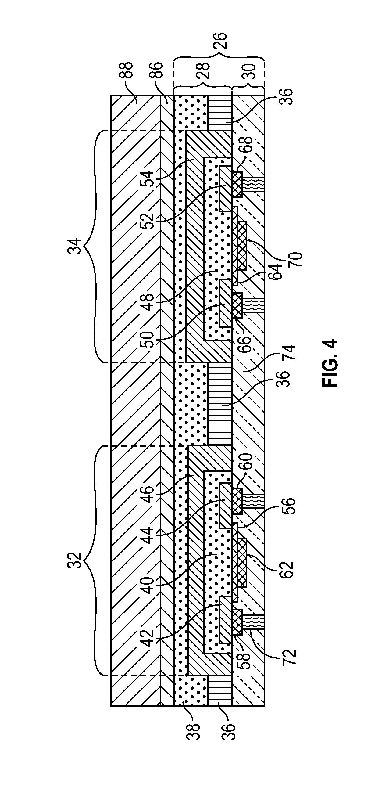
[0052] The contact layer 30 is then formed underneath the active layer 28 to complete the FEOL portion 26, as illustrated in FIG. 4. The contact layer 30 may also be formed by the CMOS process. The first (second) gate structure 56 (64) extends underneath from the first (second) N-source 42 (50) to the first (second) N-drain 44 (52). The first (second) source contact 58 (66), the first (second) drain contact 60 (68), and the first (second) gate contact 62 (70) are directly connected to and under the first (second) N-source 42 (50), the first (second) N-drain 44 (52), and the first (second) gate structure 56 (64), respectively. The first gate structure 56, the first source contact 58, the first drain contact 60, the first gate contact 62, the second gate structure 64, the second source contact 66, the second drain contact 68, and the second gate contact 70 are formed within the insulating material 74. Each via 72 extends from the first source contact 58/the first drain contact 60/the second source contact 66/the second drain contact 68 to a bottom surface of the contact layer 30.
[0053] After the FEOL portion 26 is completed, the BEOL portion 24 is formed underneath the FEOL portion 26 to provide the device region 20, as illustrated in FIG. 5. The BEOL portion 24 includes the connecting layers 76 within the dielectric layers 78. Each via 72 exposed at the bottom surface of the contact layer 30 is electrically coupled to a corresponding connecting layer 76. When the first component cell 32 and the second component cell 34 are configured to provide NFETs, the first component cell 32 and the second component cell 34 may be connected in series by one of the connecting layers 76 to form a CMOS switch. When the first component cell 32 and the second component cell 34 are configured to provide different types of FETs, the first component cell 32 and the second component cell 34 may not be electrically connected. Portions of certain ones of the connecting layers 76 are exposed through the dielectric layers 78 at the bottom surface of the BEOL portion 24. In addition, the BEOL portion 24 may further provide metal-insulator-metal (MIM) capacitors (not shown) by utilizing the connecting layers 76 and the dielectric layers 78.
[0054] The bump structures 22 are then formed at the bottom surface of the BEOL portion 24 to provide a device wafer 94, as depicted in FIG. 6. Each bump structure 22 is in contact with the exposed portion of a corresponding connecting layer 76. Herein, the bump structures 22 are electrically coupled to the first component cell 32 (the first source contact 58 in this illustration) and the second component cell 34 (the second drain contact 68 in this illustration) by the connecting layers 76 and vias 72. The bump structures 22 may be formed by a solder ball bumping technology or a copper pillar packaging technology. Each bump structure 22 protrudes from the bottom surface of the BEOL portion 24 between 20 .mu.m and 350 .mu.m. The device wafer 94 is then singulated into individual dies (not shown), each of which realizes a circuit function and includes one or more component cells in the active layer 28. Herein, an exemplary singulated device die 14F includes the device region 20 with the first component cell 32 and the second component cell 34, the bump structures 22 at the bottom of the device region 20, the interfacial layer 86 over the device region 20, and the bulk silicon handle substrate 88 over the interfacial layer 86. A top surface of the device die 14F is the backside of the bulk silicon handle substrate 88.
[0055] Next, the device die 14F is mounted to the device substrate 12 as depicted in FIG. 7. The bump structures 22 of the device die 14F are attached to the top surface of the device substrate 12, and the backside of the bulk silicon handle substrate 88 is the tallest component after the attaching process. In different applications, there may be multiple device dies mounted to the device substrate 12. The first mold compound 16 is then applied over the top surface of the device substrate 12 to provide a precursor package 96 as illustrated in FIG. 8. The device die 14F is fully encapsulated by the first mold compound 16. If there are multiple device dies mounted to the device substrate 12, the first mold compound 16 individually encapsulates each device die, and separate one from each other.
[0056] The first mold compound 16 may be applied by various procedures, such as sheet molding, overmolding, compression molding, transfer molding, dam fill encapsulation, and screen print encapsulation. The first mold compound 16 may be formed from an organic epoxy resin system or the like, such as Hitachi Chemical Electronic Materials GE-100LFC, which can be used as an etchant barrier to protect the device die 14F against etching chemistries such as KOH, NaOH, and ACH. A curing process (not shown) is followed to harden the first mold compound 16. The curing temperature may be between 100.degree. C. and 320.degree. C. depending on which material is used as the first mold compound 16.
[0057] Notice that, if the final bulk CMOS device 10 includes an underfilling layer, there may be extra steps to form the underfilling layer (not shown) before applying the first mold compound 16 over the top surface of the device substrate 12. Forming the underfilling layer is provided by applying an underfilling material over the top surface of the device substrate 12 and then curing the underfilling material to form the underfilling layer. The underfilling layer encapsulates the bump structures 22 and underfills the device die 14F between the bottom surface of the BEOL portion 24 and the top surface of the device substrate 12. The first mold compound 16 is then applied over the underfilling layer, and encapsulates at least the sides and the top surface of the device die 14F.
[0058] FIG. 9 shows a thinning procedure that the first mold compound 16 is thinned down to expose the backside of the bulk silicon handle substrate 88 of the device die 14F. The thinning procedure may be done with a mechanical grinding process. The bulk silicon handle substrate 88 is then selectively removed to provide an etched package 98, where the selective removal is stopped on the interfacial layer 86, as illustrated in FIG. 10. The removal of the bulk silicon handle substrate 88 from the device die 14F provides the thinned device die 14 and forms the opening 80 within the first mold compound 16 and over the thinned device die 14. The interfacial layer 86 is exposed at the bottom of the opening 80.
[0059] When the interfacial layer 86 is formed of SiGe, the bulk silicon handle substrate 88 may be removed by a dry etching system, such as the SELECTRA tools from Applied Materials Co. Because the interfacial layer 86 and the bulk silicon handle substrate 88 have different etching speeds, the etching system is capable of identifying the presence of the interfacial layer 88. Consequently, the etching system is able to indicate when to stop the etching process.
[0060] When the interfacial layer 86 is formed of SiGe with a Ge concentration greater than 25%, the bulk silicon handle substrate 88 may be removed by a wet etching process with TMAH. This is because a high Ge concentration (>25%) layer may effectively stop the etching process for the bulk silicon handle substrate 88 by TMAH. A wet etching process with similar appropriate silicon wet etchants or a dry etching process may also be applied to remove the bulk silicon handle substrate 88 herein.
[0061] In addition, when the interfacial layer 86 is formed of silicon with a P type dopant, such as boron, having a density greater than 1E16 cm-3 or greater than 1E18 cm-3, the bulk silicon handle substrate 88 may be removed by a wet etching process with a hydroxide base wet chemistry, such as TMAH or KOH. This is because a heavily P-doped layer may effectively stop the etching process for the bulk silicon handle substrate 88 by TMAH or KOH. A wet etching process with similar appropriate silicon wet etchants or a dry etching process may also be applied to remove the bulk silicon handle substrate 88 herein. Regardless of the material used to form the interfacial layer 86 and the etching process used to remove the bulk silicon handle substrate 88, the first mold compound 16 protects the sides and bottom surface of the thinned device die 14 from the etching process.
[0062] In some applications, the interfacial layer 86 may be also removed, as illustrated in FIG. 11. For instance, if the interfacial layer 86 is heavily doped with a P type dopant, the interfacial layer 86 may provide a pseudo ground-plane over the first component cell 32 and the second component cell 34 (switch region), which is an undesirable condition. The interfacial layer 86 may be removed by wet or dry etching chemistries in another etching process. Herein, the thinned device die 14 does not include the interfacial layer 86, and the active layer 28 is exposed at the bottom of the opening 80. If the interfacial layer 86 is formed of SiGe with a high Ge concentration (>25%), the interfacial layer 86 may be left in the thinned device die 14 and exposed at the bottom of the opening 80, since the interfacial layer 86 may be engineered to be undoped and non-conducting.
[0063] Next, the second mold compound 18 is applied over the etched package 98 to provide a mold device package 100, as illustrated in FIG. 12. The second mold compound 18 substantially fills the opening 80 and is in contact with the top surface of the thinned device die 14. Herein, substantially filling an opening refers to filling at least 75% of the entire opening. If the thinned device die 14 does not include the interfacial layer 86, the second mold compound 18 is in contact with the active layer 28. If the thinned device die 14 includes the interfacial layer 86, the second mold compound 18 is in contact with the interfacial layer 86. In either case, there is no bulk silicon handle substrate 88 left in the opening 80, such that there is no bulk silicon handle substrate 88 between the second mold compound 18 and the active layer 28. In some applications, portions of the second mold compound 18 may extend over the first mold compound 16.
[0064] The second mold compound 18 may have a superior thermal conductivity greater than 1 W/mK, or greater than 10 W/mK, and may have a dielectric constant less than 8, or between 3 and 5. The second mold compound 18 may be formed of thermoplastics or thermoset materials, such as PPS (poly phenyl sulfide), overmold epoxies doped with boron nitride, alumina, carbon nanotubes, diamond-like thermal additives, or the like. The second mold compound 18 may be formed of the same or different material as the first mold compound 16. However, unlike the second mold compound 18, the first mold compound 16 does not have thermal conductivity, electrical resistivity, or dielectric constant requirements. The second mold compound 18 may be applied by various procedures, such as compression molding, sheet molding, overmolding, transfer molding, dam fill encapsulation, and screen print encapsulation. A curing process (not shown) is followed to harden the second mold compound 18. The curing temperature is between 100.degree. C. and 320.degree. C. depending on which material is used as the second mold compound 18. After the curing process, the second mold compound 18 may be thinned and/or planarized (not shown).
[0065] Lastly, the mold device package 100 may be marked, diced, and singulated into individual devices (not shown). The bulk CMOS device 10 is an exemplary singulated device, which achieves switch functionality.
[0066] Those skilled in the art will recognize improvements and modifications to the preferred embodiments of the present disclosure. All such improvements and modifications are considered within the scope of the concepts disclosed herein and the claims that follow.
* * * * *
D00000
D00001
D00002
D00003
D00004
D00005
D00006
D00007
D00008
D00009
D00010
D00011
D00012

XML
uspto.report is an independent third-party trademark research tool that is not affiliated, endorsed, or sponsored by the United States Patent and Trademark Office (USPTO) or any other governmental organization. The information provided by uspto.report is based on publicly available data at the time of writing and is intended for informational purposes only.
While we strive to provide accurate and up-to-date information, we do not guarantee the accuracy, completeness, reliability, or suitability of the information displayed on this site. The use of this site is at your own risk. Any reliance you place on such information is therefore strictly at your own risk.
All official trademark data, including owner information, should be verified by visiting the official USPTO website at www.uspto.gov. This site is not intended to replace professional legal advice and should not be used as a substitute for consulting with a legal professional who is knowledgeable about trademark law.