Substrate Rack And A Substrate Processing System And Method
Pierreux; Dieter ; et al.
U.S. patent application number 15/940759 was filed with the patent office on 2019-10-03 for substrate rack and a substrate processing system and method. The applicant listed for this patent is ASM IP Holding B.V.. Invention is credited to Cornelis Thaddeus Herbschleb, Bert Jongbloed, Werner Knaepen, Dieter Pierreux, Hessel Sprey.
| Application Number | 20190304821 15/940759 |
| Document ID | / |
| Family ID | 68055086 |
| Filed Date | 2019-10-03 |

| United States Patent Application | 20190304821 |
| Kind Code | A1 |
| Pierreux; Dieter ; et al. | October 3, 2019 |
SUBSTRATE RACK AND A SUBSTRATE PROCESSING SYSTEM AND METHOD
Abstract
The invention relates to a substrate rack and a substrate processing system for processing substrates in a reaction chamber. The substrate rack may be used for introducing a plurality of substrates in the reaction chamber. The substrate rack may have a plurality of spaced apart substrate holding provisions configured to hold the substrates in a spaced apart relationship. The rack may have an illumination system to irradiate radiation with a range from 100 to 500 nanometers onto a top surface of the substrates.
| Inventors: | Pierreux; Dieter; (Dilbeek, BE) ; Knaepen; Werner; (Leuven, BE) ; Jongbloed; Bert; (Oud-Heverlee, BE) ; Herbschleb; Cornelis Thaddeus; (Leiden, NL) ; Sprey; Hessel; (Kessel-Lo, BE) | ||||||||||
| Applicant: |
|
||||||||||
|---|---|---|---|---|---|---|---|---|---|---|---|
| Family ID: | 68055086 | ||||||||||
| Appl. No.: | 15/940759 | ||||||||||
| Filed: | March 29, 2018 |
| Current U.S. Class: | 1/1 |
| Current CPC Class: | H01L 21/6719 20130101; H01L 21/67063 20130101; H01L 21/30604 20130101; H01L 21/67346 20130101; C23C 16/482 20130101; H01L 21/67115 20130101; H01L 21/67757 20130101; H01L 21/0223 20130101; C23C 16/56 20130101; C23C 16/4583 20130101 |
| International Class: | H01L 21/673 20060101 H01L021/673; H01L 21/306 20060101 H01L021/306; H01L 21/02 20060101 H01L021/02; C23C 16/48 20060101 C23C016/48; H01L 21/67 20060101 H01L021/67 |
Claims
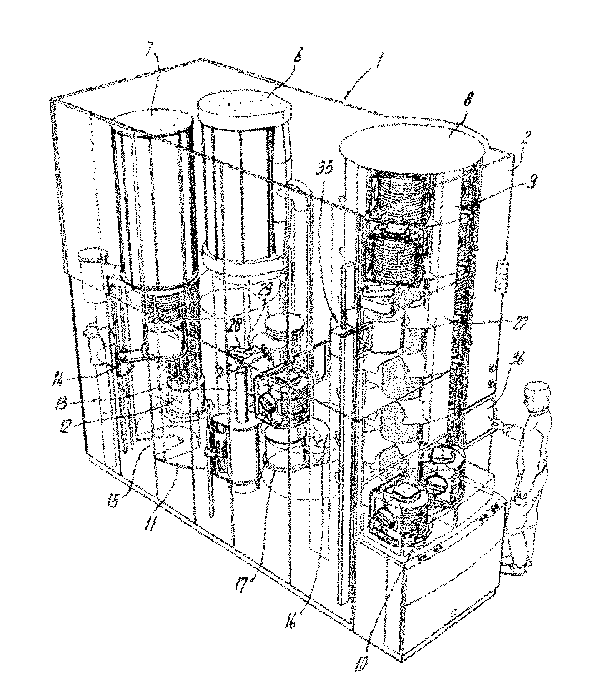
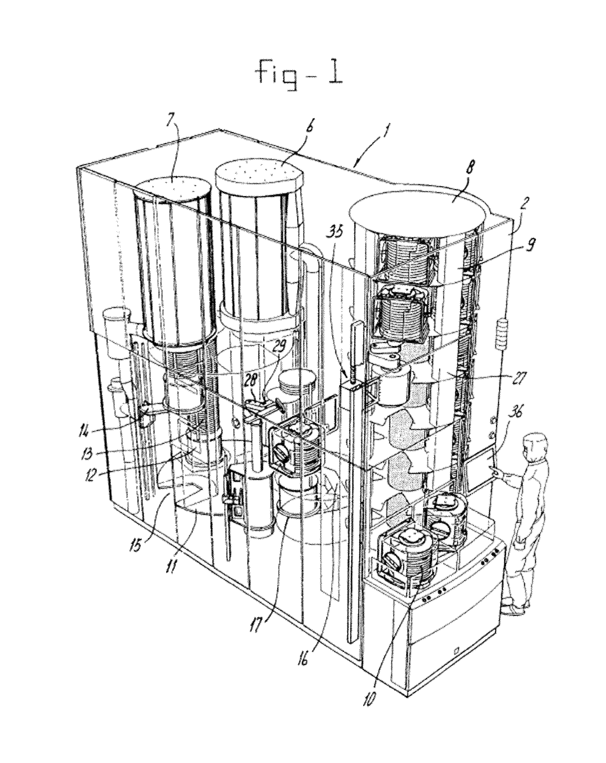
1. A substrate rack constructed for holding a plurality of substrates in a reaction chamber of a substrate processing system, the substrate rack comprising a plurality of spaced apart substrate holding provisions configured to hold the plurality of substrates in a spaced apart relationship, wherein the substrate rack comprises an illumination system constructed and arranged to radiate ultraviolet radiation with a range from 100 to 500 nanometers onto a top surface of at least one of the substrates held in the substrate holding provisions.
2. The rack according to claim 1, wherein the substrate holding provisions of the rack are constructed and arranged to hold the top surface of the at least one of the substrates opposite a radiation output surface of the illumination system so as to radiate ultraviolet radiation onto the top surface of the at least one of the substrates.
3. The rack according to claim 1, wherein the illumination system comprises a plurality of illumination devices provided to the rack and each illumination device has dedicated substrate holding provisions on the rack to hold the top surface of one of the substrates in the radiation of the illumination device.
4. The rack according to claim 3, wherein the dedicated substrate holding provisions on the rack are configured to hold one substrate in between two illumination devices.
5. The rack according to claim 3, wherein the illumination device comprises a substantially plate shape with a top and a back surface and the back surface comprises a radiation output surface.
6. The rack according to claim 3, wherein the illumination device has substantially the same size as the substrate in directions parallel to the top surface.
7. The rack according to claim 3, wherein the illumination device is provided with illumination sources irradiating ultraviolet radiation onto the top surface of at least one of the substrates in the substrate rack.
8. The rack according to claim 7, wherein the illumination device comprises a first light emitting diode for irradiating ultraviolet radiation within a range from 100 to 500 nanometers.
9. The rack according to claim 7, wherein the illumination device comprise a second light emitting diode for irradiating infrared radiation within a range from 700 nanometers to 1 millimeter to heat the substrate.
10. The rack according to claim 1, wherein the illumination system is passive and is constructed and arranged to direct radiation from outside the rack to the substrates.
11. The rack according to claim 1, wherein the illumination system comprises an optical wave guide to guide the radiation to the substrates.
12. The rack according to claim 11 wherein the optical wave guide is an optical fiber.
13. The rack according to claim 1, wherein the illumination system is provided with radiation reflecting surfaces to direct the ultraviolet radiation to the substrates.
14. The rack according to claim 13, wherein the radiation reflecting surfaces comprises a material selected from the group of material comprising glass, steel, aluminum or polytetrafluoroethylene (PTFE) to direct the radiation to the substrates.
15. The rack according to claim 13, wherein the radiation reflecting surfaces comprises a scatter plate to scatter the radiation to the substrates.
16. The rack according to claim 1, wherein the illumination system is constructed and arranged to direct the radiation in a direction within 0-45 degrees of an axis perpendicular to the top surface of the at least one of the substrates.
17. The rack according to claim 1, wherein the rack is provided with an electrical power connection and the illumination system is active and constructed and arranged to generate radiation from the electrical power and direct the radiation to the substrates.
18. The rack according to claim 17, wherein the illumination system comprises a discharge lamp.
19. The rack according to claim 1, wherein the rack is provided with a gas supply system for providing a gas flow on a radiation transmitting or reflecting surface.
20. The rack according to claim 2, wherein the illumination system comprises multiple parts to irradiate ultraviolet radiation to the substrates in the substrate rack from multiple sides.
21. The rack according to claim 1, wherein the rack is constructed and arranged for movement in a reaction chamber.
22. A substrate processing system comprising: a reaction chamber constructed an arranged to process a plurality of substrates in a rack according to claim 1; and a rack handler constructed and arranged to move the rack into the reaction chamber.
23. The substrate processing system according to claim 22, wherein the system comprises a rotation device for rotating the rack with substrates around a vertical axis in the reaction chamber.
24. The substrate processing system according to claim 22, wherein the reaction chamber is limited by a process tube and the system comprises a UV radiation system constructed and arranged to irradiate the ultraviolet radiation through the process tube into the reaction chamber to the illumination system of the rack and the illumination system is passive and is constructed and arranged to direct radiation from outside the rack to the substrates.
25. The substrate processing system according to claim 22, wherein the rack is provided with an electrical power connection which is electrically connected to the rest of the substrate processing system to supply energy to the rack.
26. A substrate processing method, comprising: providing a plurality of substrates in a substrate rack comprising a plurality of spaced apart substrate holding provisions configured to hold the plurality of substrates in a spaced apart relationship; moving the rack with substrates in a reaction chamber; and, irradiating ultraviolet radiation with a range from 100 to 500 nanometers to a top surface of at least one of the substrates held in the substrate rack from an illumination system provided to the rack.
27. The substrate processing method according to claim 26, wherein irradiating ultraviolet radiation to the substrates in the substrate rack comprises directing the ultraviolet radiation to the substrates via a radiation transmitting or reflecting surface.
28. The substrate processing method according to claim 26, wherein the method comprises providing a fluid into the reaction chamber via an inlet.
29. The substrate processing method according to claim 28, wherein the method comprises providing a fluid with a precursor into the reaction chamber via the inlet to deposit a layer on the substrates.
30. The substrate processing method according to claim 28, wherein the method comprises providing an oxidizing fluid in the reaction chamber so as to oxidize a layer deposited on the radiation transmitting or reflecting surface to improve the transmissivity of the radiation transmitting or reflecting surface.
31. The substrate processing method according to claim 28, wherein the method comprises providing an etching fluid in the reaction chamber so as to etch a layer deposited on the radiation transmitting or reflecting surface away to improve the transmissivity of the radiation transmitting or reflecting surface.
Description
FIELD
[0001] The present invention generally relates to a substrate rack, and a substrate processing system and method. More particularly, the invention relates to a substrate rack constructed for holding a plurality of substrates in a reaction chamber of a substrate processing system during a substrate processing method. The substrate rack may comprise a plurality of spaced apart substrate holding provisions configured to hold the plurality of substrates in a spaced apart relationship.
BACKGROUND
[0002] Furnaces, functioning as reactors, may be used as reaction chambers to create fine dimension structures, such as integrated circuits, on a substrate. Several substrates, such as silicon wafers, may be placed on a substrate holder, such as a substrate rack or boat and moved inside the reactor. In a subsequent substrate treatment step the substrates may be heated. Further, reactant gases may be passed over the substrate, causing the deposition of a thin layer of the reactant material or reactants of the gases on the substrate to be treated.
[0003] A series of treatment steps on a substrate is called a recipe. If the deposited layer has the same crystallographic structure as the underlying silicon substrate, it is called an epitaxial layer. This is also sometimes called a monocrystalline layer because may have one crystal structure. Through subsequent deposition, doping, lithography, etch and other processes, these layers are made into integrated circuits, producing from tens to thousands or even millions of integrated devices, depending on the substrate size and the circuits' complexity.
[0004] Various process parameters are carefully controlled to ensure the high quality of the resulting layers. One such critical parameter is the substrate temperature during each recipe step. During CVD, for example, the deposition gases react within a particular temperature window and deposit on the substrate. Different temperatures result in different deposition rates and quality. Accordingly, it is important to accurately control the substrate temperature to bring the substrate to the desired temperature before the reaction treatment begins. The substrate may comprise features that are temperature sensitive and therefor the temperature may be limited to a certain maximum to avoid damage to those sensitive features.
[0005] For certain processes energy may be necessary at the substrate surface. If this energy is provided in the form of heat this may lead to contradicting requirements in which for productivity, quality and/or reactivity the temperature should be high, while to avoid damage to the features on the substrate the temperature should remain low.
SUMMARY
[0006] Accordingly, there may be a need for providing energy to a surface of a plurality of substrates in a reaction chamber.
[0007] In accordance with at least one embodiment of the invention there may be provided a substrate rack. The substrate rack may be constructed for holding a plurality of substrates in a reaction chamber of a substrate processing system. The substrate rack may comprise a plurality of spaced apart substrate holding provisions configured to hold the plurality of substrates in a spaced apart relationship. The substrate rack may comprise an illumination system constructed and arranged to radiate ultraviolet radiation with a range from 100 to 500 nanometers onto a top surface of at least one of the substrates held by the substrate holding provisions.
[0008] By irradiating the surface of the substrates with ultraviolet radiation, it may be possible to provide energy to the top surface. The illumination system may be constructed and arranged to radiate ultraviolet radiation with a range from 100 to 500, preferably 150 to 400, and even more preferably 170 to 300 nanometers. The spaced apart substrate holding provisions of the substrate rack may be configured to independently hold a substrate in a particular orientation.
[0009] In accordance with a further embodiment of the invention there may be provided a substrate processing system comprising:
[0010] a reaction chamber constructed and arranged for processing a plurality of substrates in a rack; and
[0011] a rack handler for moving the rack into the reaction chamber. The rack may comprise an illumination system constructed and arranged to radiate ultraviolet radiation with a range from 100 to 500 nanometers from a radiation output surface onto a top surface of at least one of the substrates held by the substrate holding provisions. The rack may comprise a plurality of spaced apart substrate holding provisions configured to hold the plurality of substrates in a spaced apart relationship.
[0012] According to yet a further embodiment there is provided a substrate processing method, comprising:
[0013] providing a plurality of substrates in a substrate rack comprising a plurality of spaced apart substrate holding provisions configured to hold the plurality of substrates in a spaced apart relationship;
[0014] moving the rack with substrates in a reaction chamber; and,
[0015] irradiating ultraviolet radiation with a range from 100 to 500 nanometers to a top surface of at least one of the substrates held in the substrate rack from an illumination system provided to the rack.
[0016] The method may comprise providing a fluid into the reaction chamber via an inlet. The fluid may be used to deposit a layer on the substrates.
[0017] Alternatively, a fluid may be used to improve the transmissivity of the radiation transmitting or reflecting surface. The fluid may be an oxidizing fluid used to oxidize a layer deposited on the radiation transmitting or reflecting surface to improve the transmissivity of the radiation transmitting or reflecting surface. The fluid may be an etching fluid so as to etch a layer deposited on the radiation transmitting or reflecting surface away to improve the transmissivity of the radiation transmitting or reflecting surface.
[0018] For purposes of summarizing the invention and the advantages achieved over the prior art, certain objects and advantages of the invention have been described herein above. Of course, it is to be understood that not necessarily all such objects or advantages may be achieved in accordance with any particular embodiment of the invention. Thus, for example, those skilled in the art will recognize that the invention may be embodied or carried out in a manner that achieves or optimizes one advantage or group of advantages as taught or suggested herein without necessarily achieving other objects or advantages as may be taught or suggested.
[0019] All of these embodiments are intended to be within the scope of the invention herein disclosed. These and other embodiments will become readily apparent to those skilled in the art from the following detailed description of certain embodiments having reference to the attached figures, the invention not being limited to any particular embodiment(s) disclosed.
BRIEF DESCRIPTION OF THE FIGURES
[0020] It will be appreciated that elements in the figures are illustrated for simplicity and clarity and have not necessarily been drawn to scale. For example, the dimensions of some of the elements in the figures may be exaggerated relative to other elements to help improve understanding of illustrated embodiments of the present disclosure.
[0021] FIG. 1 shows a perspective view of the substrate processing system with the substrate rack according to an embodiment;
[0022] FIG. 2 shows a plan top view of the system according to FIG. 1; and
[0023] FIGS. 3A, 3B and 3C show a perspective view of a substrate rack with substrates that are illuminated with an illumination system according to a first (A) and a second (B) embodiment.
DETAILED DESCRIPTION
[0024] Although certain embodiments and examples are disclosed below, it will be understood by those in the art that the invention extends beyond the specifically disclosed embodiments and/or uses of the invention and obvious modifications and equivalents thereof. Thus, it is intended that the scope of the invention disclosed should not be limited by the particular disclosed embodiments described below.
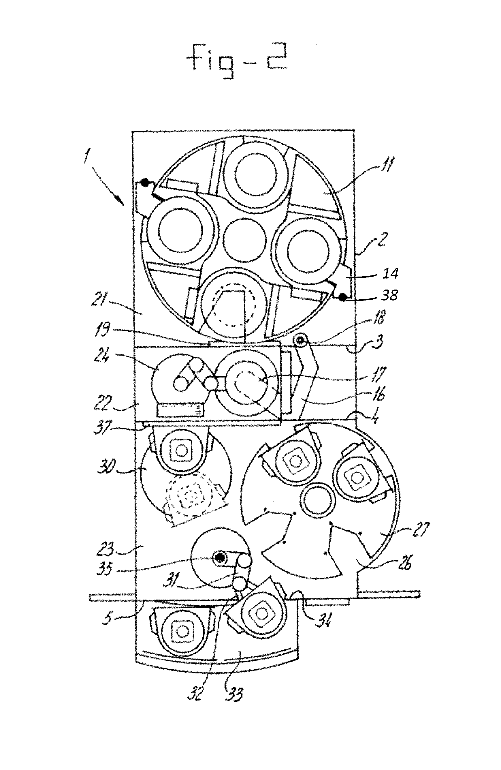
[0025] A substrate processing system with a substrate rack according to an embodiment may be indicated in FIGS. 1 and 2. Said system may be incorporated in an apparatus 1 comprising a housing 2 and may in general being installed partially or completely in a so-called "clean room".
[0026] In addition to housing 2, partitions 3, 4 and 5 may be present, as can be seen in particular from FIG. 2. Housing 2 may delimit, with partition 3, reactor area 21. A substrate handling chamber 22 may be delimited between housing 2 and partitions 3, 4. A cassette handling chamber 23 may be delimited between partitions 4 and 5 and housing 2. The apparatus 1 may further comprise a cassette introduction portion 33.
[0027] Two reactor chambers 6, 7, may be arranged in reactor area 21, however also a single reactor chamber may be used. Said reactor chambers may be positioned vertically and substrate racks 12 filled with substrates 13, e.g., semiconductor wafers, may be moved into the reactor chambers 6, 7 in the vertical direction from below.
[0028] The substrate racks 12 may comprise a plurality of spaced apart substrate holding provisions configured to hold the plurality of substrates 13 in a spaced apart relationship. The substrate rack 12 may be supported at the bottom on an insulating plug, which provides a seal with respect to the reactor chamber 6, 7.
[0029] Each reactor chamber 6, 7 may have a rack handler comprising an insertion arm 14, which is movable in the vertical direction with the aid of a spindle 38, to bring the substrate rack 12 in the reactor chamber. In FIG. 2 it is indicated that there may be two insertion arms 14 on both sides of the apparatus. The reactor chamber may be referred to as a furnace and may be provided with a heater to heat the substrates.
[0030] The rack handler further may comprise a rotary platform 11, provided with cut-outs 15, arranged in the reaction area 21. Said cut-outs 15 may be shaped such that, if the cut-outs 15 have been brought into the correct position, arm 14 is able to move up and down through the cut-outs. On the other hand, the diameter of the bottom of the substrate rack may be such that said diameter is larger than the cut-out 15 in the platform 11, so that when the arm 14 moves downwards from the position shown in FIG. 1 the substrate rack 12 may be placed on rotary platform 11 and may be removed therefrom again in a reverse operation.
[0031] The substrate racks 12 may be fed to both reactor chambers 6 and 7 with the rack handler. It may be possible to perform a successive treatment therein. It may also be possible to allow parallel groups of substrate racks 12 to be treated exclusively by reactor chamber 6 and exclusively by reactor chamber 7. Said substrate racks 12 may be provided with substrates 13. The system comprises a rotation device for rotating the rack 12 with substrates 13 around a vertical axis in the reaction chamber 6, 7 to improve the uniformity of the treatment.
[0032] Substrates 13 may be supplied in (transport) cassettes 10 which, from the cassette introduction portion 33, may be placed in store 8 through a closable opening 34 with the aid of arm 31 of the cassette handling robot 35. Arm 31 may be provided with a bearing surface 32 which has dimensions a little smaller than those of the series of cut-outs 26 in rotary platforms 27. A number of such rotary platforms may be provided one above the other in the vertical direction in store 8. Arm 31 may be movable in the vertical direction with the aid of cassette handling robot 35. Arm 31 may be mounted such that said arm is able not only to pick up or remove cassettes from or to introduction portion 33 to or from store 8, but also to make it possible to move cassettes from or to store 8 to or from rotary platform 30.
[0033] Said rotary platform 30 may be constructed such that on rotation the cassette is placed against partition 4 where an opening 37 has been made so that, after opening the cassettes, substrates can be taken one by one from the cassette concerned with the aid of arm 24 of a substrate handler and can be placed in the substrate rack 12 located in substrate handling chamber 22.
[0034] Said substrate rack 12 is supported by a hinged arm 16 being part of the rack handler and provided with a bearing surface 17 at the end, the dimensions of which are somewhat smaller than those of cut-outs 15 of rotary platform 11. Said arm 16 may be able to move with the substrate rack through a closable opening in partition 3 by rotation about rotation point 18. A closure may be provided in order to be able to close opening 19 between reaction area 21 and substrate handling chamber 22.
[0035] An operator or an automated cassette transport system (not shown), may load store 8 by introducing a number of cassettes on introduction portion 33. Control operations may be done on panel 36. Cassettes 10 may be transferred from the introduction portion 33 with the aid of arm 31 into the storage compartments 9 made for these cassettes in store 8. By starting from the lowest position for removing the relevant cassette 10 from portion 33 through the opening 34, said cassette can be moved upwards for moving into a higher compartment 9 of the store 8 by the cassette handling robot 35. By rotation of the store 8 it is possible to fill various compartments 9 with cassettes 10.
[0036] The cassettes 10 concerned may be removed from the store by arm 31 and placed on rotary platform 30. The cassettes are rotated on the rotary platform 30 and placed with their door against partition 4. The door of the cassette may be removed with a door opener. With the aid of arm 24, the substrates may be removed substrate by substrate and placed in substrate rack 12 placed on swing arm 16 with the substrate handler.
[0037] In the interim the rotary platform 11 may be able to move in the reactor area 21 in an optimum manner with regard to the treatments to be carried out on the substrates present inside the reactor area 21. After substrate rack 12 has been filled in the substrate handling chamber 22 and may become available to one of the reactor chambers 6, 7, opening 19, which was closed up to this time, is opened and said freshly filled substrate rack 12 may be placed on rotary platform 11. Said rotary platform 11 may then move one position and the filled substrate rack 12 may be removed from platform 11 with the help of insertion arm 14 into the reactor chambers 6, 7. Treated substrates in a finished rack may be lowered on said filled platform 11. Said substrates execute a movement counter to the above to end up in the cassettes.
[0038] The substrate rack 12 with the fresh substrate may be fed to reactor chamber 6 or 7 with the insertion arms 14 and may be treated in said chamber. It may be possible to perform a successive treatment in the reactor chamber 6, 7. As depicted the apparatus may have two reactor chambers 6, 7, but the apparatus may have also one reactor chamber or three or more reactor chambers without departing from the scope of invention.
[0039] The treatment may comprise an increase of the temperature of the substrates in the substrate rack 12 with a heater. The increased temperature may be necessary to get the right reactivity. It is therefore important to accurately control the substrate temperature to bring the substrate to the desired temperature before the treatment begins to get the right reactivity and productivity. Further the substrate may comprise features that are temperature sensitive and therefor the temperature may be limited to a certain maximum to avoid damage to those sensitive features. This may lead to contradicting requirements in which for reactivity the temperature requirements of the substrate may be high while the temperature requirement of the substrate may be limited to avoid damaging the temperature sensitive features on the substrate.
[0040] FIGS. 3A and 3B show a cross-section of a substrate rack 12 with a substrates 13. The substrate rack 12 may comprise a top plate 41 connected with struts 43 to a bottom plate 45. A plurality of spaced apart substrate holding provisions 47 configured to hold the plurality of substrates 13 in a spaced apart relationship may be provided to the struts 43. In general 2 to 4 struts may be provided in a rack 12 and 10 to 200 substrate holding provisions 47 may be provided to hold substrates 13. The rack 12 may be supported by an insulating plug 49 which provides a seal with respect to the reactor chamber 6, 7 at the bottom.
[0041] The substrate rack 12 may be provided with an illumination system constructed and arranged to radiate ultraviolet radiation with a range from 100 to 500 nanometers onto a top surface of at least one of the substrates 13 held in the substrate holding provisions 47. The illumination system may be constructed and arranged to radiate ultraviolet radiation with a range from 100 to 500, preferably 150 to 400, and even more preferably 170 to 300 nanometers. The substrate holding provisions 47 of the rack 12 may be constructed and arranged to hold the top surface of the at least one of the substrates opposite a radiation output surface of the illumination system so as to radiate ultraviolet radiation onto the top surface of the at least one of the substrates.
[0042] By irradiating the top surface of the substrates with ultraviolet radiation it may be possible to provide energy to the top surface for certain processes. The energy may increase the reactivity on the top surface. This increase of reactivity may be accomplished while not overheating the substrate so that temperature sensitive features on the substrate may not get damaged. The increase of reactivity may lead to a better quality of the deposited layer and/or a higher productivity of the apparatus. It may also lead to certain processes becoming possible at a temperature on which before they were not possible because the reactivity was zero.
[0043] The illumination system may comprise a plurality of illumination devices 51 provided to the rack 12. Each illumination device 51 may have dedicated substrate holding provisions 47 on the rack to hold the top surface of one of the substrates in the radiation of the illumination device.
[0044] The energy transfer from an electromagnetic wave (like UV) unto the top surface of the substrate is proportional to the cosines of the angle between an axis perpendicular to the top surface of the substrate and the direction of the radiation. The illumination device may therefore be constructed and arranged to direct the radiation in a direction within 0-60 degrees, preferably 0-45 degrees, more preferably 0-30 degrees and most preferably 0-15 degrees of an axis perpendicular to the top surface of the substrate on the top surface of the substrate. Further, it may be difficult to direct direction to deep trenches that may be formed in the microstructures on the top surface of the substrate. Radiation in a direction with smaller angles with an axis perpendicular to the top surface of the substrate may increase the in coupling of the radiation into deep trenches.
[0045] The dedicated substrate holding provisions 47 provided to the rack 12 may be configured to hold one substrate in between two illumination devices. The illumination device 51 may have a substantially plate shape with a top and a back surface. The back surface may comprise the radiation output surface. The illumination device 51 may have substantially the same size as the substrate 13 in directions parallel to the substrate surface.
[0046] FIG. 3C depicts an enlargement of the illumination device 51 of FIG. 3A. The illumination device 51 which may be provided with illumination sources 53, 55. Some illumination sources 53 may irradiate ultraviolet radiation onto the top surface of at least one of the substrates in the substrate rack 12. The illumination sources 53 comprise a first light emitting diode for irradiating ultraviolet radiation within a range from 100 to 500, preferably 150 to 400, and even more preferably 170 to 300 nanometers. Other illumination sources 55 comprise a second light emitting diode for irradiating infrared radiation within a range from 700 nanometers to 1 millimeter to heat the substrate.
[0047] In FIG. 3B the illumination device 51 is provided with illumination sources 53 only comprising a first light emitting diode for irradiating ultraviolet radiation within a range from 100 to 500 nanometers. The heating function in FIG. 3B is accomplished by the heater provided with heating coils 51. Beside the heating function, FIG. 3A and FIG. 3B are identical and function in conjunctions with each other so that FIG. 3B functions as the lower part of the FIG. 3A and the other way around.
[0048] The rack 12 may be provided with an electrical power connection 57 connectable to a power source V. The rack could, for example, have a power connector. The power connector may have a plug and socket connection. The illumination system may be active and constructed and arranged to generate radiation from the electrical power and direct the radiation to the substrates. The illumination devices 51 may comprise a gas discharge lamp or a light emitting diode to generate radiation from the electrical power.
[0049] Gas discharge lamps generate radiation by having an electric discharge between two electrodes through an ionized gas, e.g., a plasma in a tube. Such lamps may use a noble gas such as argon, neon, krypton, and xenon or a mixture thereof and additionally even may use mercury, sodium, and metal halides in the mixture in the tube. The electrons may be forced to leave atoms of the gas near an anode by the electric field applied between the two electrodes from which only one 45 is depicted, leaving these atoms positively ionized. Free electrons flow to the anode, while the cations flow to the cathode. The ions may collide with neutral gas atoms, which transfer their electrons to the ions. The atoms, having lost an electron during the collisions, ionize and speed toward the cathode while the ions, having gained an electron during the collisions, return to a lower energy state while releasing energy in the form of radiation which is emitted in the direction of the substrate top surface of the substrate to transfer its energy into the top surface.
[0050] The rack 12 may be provided with a passive illumination device constructed and arranged to direct radiation from outside the rack to the substrates. The active components of the illumination source may be provided outside the reaction chamber in the apparatus and direct the radiation to the passive illumination device provided in the rack. The passive components in the reaction chamber may be less sensitive to the hot and reactive environment in the reaction chamber than the active components.
[0051] The passive illumination device may comprise an optical wave guide to guide the radiation to the substrates. The optical wave guide may be an optical fiber. The optical wave guide may be hollow.
[0052] The passive illumination device may be provided with radiation reflecting surface to direct the ultraviolet radiation to the substrates. The radiation reflecting surface may comprise a mirror to redirect the radiation to the substrates. The radiation reflecting surface may be made of glass, steel, aluminum or polytetrafluoroethylene (PTFE) to reflect ultraviolet radiation. The radiation reflecting surface may have an upside down cone shape to reflect ultraviolet radiation from the side of the rack downwards to the substrate surface. The radiation reflecting surface may comprise a scatter plate to scatter the radiation to the substrates.
[0053] The rack 12 may be provided with a gas supply system for providing a gas flow on a radiation transmitting or reflecting surface. In this way deposition of contamination on the radiation transmitting or reflecting surface may be circumvented. The illumination system may comprise multiple parts to irradiate ultraviolet radiation to the substrates in the substrate rack from multiple sides.
[0054] The illumination system for illuminating the substrate surface may have a power of between 5 W and 100 kW, preferably 300 W and 20 kW and even more preferably between 1 and 10 kW. The illumination devices for illuminating the substrate surface may have a power of between 0.05 and 150 W, preferably 1 W and 60 W and even more preferably between 4 and 50 W. The illumination system may have an efficiency of between 50 and 90% in the conversion of electrical energy to ultraviolet radiation. The substrate surface may receive a power between 0.1 and 200 milliwatt (mW)/cm.sup.2, preferably between 1 and 100 mw/cm.sup.2 and even more preferably between 5 and 80 mW/cm.sup.2.
[0055] The rack 12 may have a length between 50 and 200 cm and may be between 20 and 50 cm, preferably around 30 cm wide. The rack 12 may have a maximum of between 20 and 120, preferably between 40 and 80 spaced apart substrate holding provisions along the struts for holding an equal amount of substrates. The rack 12 may be provided with between 20 and 130, preferably between 40 and 80 illumination devices 51. The distance between the substrates 13 and the illumination devices 51 in the rack 12 may be between 4 to 20, preferably 5 to 10 mm.
[0056] The apparatus may be provided with at least one fluid inlet 59. The fluid inlet 59 may be embodied as an injector within the reaction chamber for providing a fluid into the reaction chamber. A purge or processing gas may be provided through the inlet 59. The apparatus may be provided with a fluid system comprising a control system for controlling a valve for providing the fluid such as a processing or purge gas in the reaction chamber via the inlet. The fluid may be received from a fluid storage or a gas line.
[0057] The control system and the valve may be constructed and arranged to process substrates. More particularly the control system and the valve may be constructed and arranged to perform an atomic layer deposition (ALD) or chemical vapor deposition (CVD) cycle on the substrate with a first and/or second precursor stored in a fluid storage. The apparatus may be provided with a fluid outlet 61 to remove gases from the reaction chamber 6, 7. The ultraviolet radiation can be used to deposit or densify, atomic (ALD) layers, chemical vapor deposition (CVD) layers or other layers.
[0058] When layers of, for example, silicon or silicon nitride are deposited in a reaction chamber 6, 7, the efficiency of the ultraviolet radiation system may be reduced by absorption when a thickness of deposited material is adding up on top of the radiation transmitting surface. Purging the radiation transmitting surfaces may be alleviating this issue to some extent.
[0059] A complementary periodical in situ clean with etch gases may be a required to clean the radiation transmitting or reflecting surface of the illumination devices 51. The apparatus may comprise an etching system. The etching system may comprise a fluid storage, a control system and a valve. The control system may be provided with a program when run on the control system to improve the transmissivity of the radiation transmitting or reflecting surface after a layer is deposited on the radiation transmitting or reflecting surface.
[0060] An etching fluid may be stored in the fluid storage of the etching system. The control system may be controlling a valve for providing the etching fluid in the reaction chamber 6, 7 via the inlet 59. The control system may control the valve to provide the etching fluent i.e., etchant in the reaction chamber, so as to etch a layer deposited on the radiation transmitting or reflecting surface away to improve the transmissivity of the surface.
[0061] The etching fluid may be chloride (Cl2), boriumchloride (BCl3), hydrogenchloride (HCl), tetrafluoromethane (CF4), nitrogentrifluoride (NF3), hydrogenbromide (HBr), sulfur hexafluoride (SF6), or an ashing component created by ultraviolet radiation in combination with an hydrogen or oxygen comprising gas such as hydrogen or oxygen. The periodical in situ clean with etch gases may also be used as an alternative for purging the radiation transmitting or reflecting surfaces which may simplify the design of the apparatus.
[0062] The radiation transmitting surface or reflecting surface may also be made transmissive or reflective for the illumination radiation again by periodically converting the silicon or silicon nitride layers into silicon oxide by a thermal treatment in an oxidizing environment. The apparatus may comprise a conversion system. The conversion system may comprise the fluid storage, the control system and the valve. The control system may be provided with a program when run on the control system to improve the transmissivity of the radiation transmitting or reflecting surface after a layer is deposited on the radiation transmitting or reflecting surface.
[0063] An oxygen comprising fluid, such as, for example, oxygen (O.sub.2), ozone (O.sub.3), peroxide (H.sub.2O.sub.2), water (H.sub.2O), or nitrous oxide (N.sub.2O), may for this purpose be stored in the fluid storage. The control system may be controlling a valve for providing the oxidizing fluid in the reaction chamber 6, 7 via the inlet 59 from the fluid storage and controlling heating of the reaction chamber. After conversion of the silicon or silicon nitride layers into silicon oxide the silicon oxide may transmit the UV and no in situ clean may be required. The periodical in situ conversion with oxidizing gas may also be used as an alternative for purging the radiation transmitting or reflecting surfaces which may simplify the design of the apparatus.
[0064] The substrate 13 may be positioned in the substrate rack 12 having three struts 43 comprising a plurality of spaced apart substrate holding provisions 47 configured to hold the plurality of substrates 13 in a spaced apart relationship. The struts 43 may be elongated and extend in a direction substantially perpendicular to the substrate surface, e.g., in a vertical direction. The plurality of substrates may be positioned parallel in the substrate rack 12. The top plate 41 and the bottom plate 45 may extend parallel to the substrates in a horizontal direction.
[0065] Alternatively, a rack 12 may be filled with substrates to be processed alternating with removable illumination devices 51 which are also positioned in the rack. The removable illumination devices could, for example, have their own independent power supply or a power connector. The independent power supply could be a working with a chargeable battery, or an RF receiver. The power connector may have a plug and socket connection with the rack or a part of the apparatus. The substrate handler may be used to fill the rack 12 with the substrates 13 to be processed alternating with the removable illumination devices 51. The removable illumination devices could be switched on after the rack is moved into the reactor. The removable illumination devices 51 may be removed from the rack and cleaned after the rack is moved out of the reaction chamber. Removable illumination devices create a very versatile system.
[0066] The particular implementations shown and described are illustrative of the invention and its best mode and are not intended to otherwise limit the scope of the aspects and implementations in any way. Indeed, for the sake of brevity, conventional manufacturing, connection, preparation, and other functional aspects of the system may not be described in detail. Furthermore, the connecting lines shown in the various figures are intended to represent exemplary functional relationships and/or physical couplings between the various elements. Many alternative or additional functional relationship or physical connections may be present in the practical system, and/or may be absent in some embodiments.
[0067] It is to be understood that the configurations and/or approaches described herein are exemplary in nature, and that these specific embodiments or examples are not to be considered in a limiting sense, because numerous variations are possible. The specific routines or methods described herein may represent one or more of any number of processing strategies. Thus, the various acts illustrated may be performed in the sequence illustrated, in other sequences, or omitted in some cases.
[0068] The subject matter of the present disclosure includes all novel and nonobvious combinations and sub combinations of the various processes, systems, and configurations, and other features, functions, acts, and/or properties disclosed herein, as well as any and all equivalents thereof.
* * * * *
D00000
D00001
D00002
D00003
XML
uspto.report is an independent third-party trademark research tool that is not affiliated, endorsed, or sponsored by the United States Patent and Trademark Office (USPTO) or any other governmental organization. The information provided by uspto.report is based on publicly available data at the time of writing and is intended for informational purposes only.
While we strive to provide accurate and up-to-date information, we do not guarantee the accuracy, completeness, reliability, or suitability of the information displayed on this site. The use of this site is at your own risk. Any reliance you place on such information is therefore strictly at your own risk.
All official trademark data, including owner information, should be verified by visiting the official USPTO website at www.uspto.gov. This site is not intended to replace professional legal advice and should not be used as a substitute for consulting with a legal professional who is knowledgeable about trademark law.