Plasma Processing Apparatus And Method For Manufacturing Mounting Stage
SASAKI; Yasuharu ; et al.
U.S. patent application number 16/282552 was filed with the patent office on 2019-08-29 for plasma processing apparatus and method for manufacturing mounting stage. The applicant listed for this patent is Tokyo Electron Limited. Invention is credited to Ryo CHIBA, Akira NAGAYAMA, Yasuharu SASAKI.
| Application Number | 20190267277 16/282552 |
| Document ID | / |
| Family ID | 67686112 |
| Filed Date | 2019-08-29 |


| United States Patent Application | 20190267277 |
| Kind Code | A1 |
| SASAKI; Yasuharu ; et al. | August 29, 2019 |
PLASMA PROCESSING APPARATUS AND METHOD FOR MANUFACTURING MOUNTING STAGE
Abstract
A plasma processing apparatus includes a mounting stage including a mounting surface, on which an object to be processed is mounted, a back surface provided on a side opposite to the mounting surface, a plate-like member, in which a first hole penetrating through the mounting surface and the back surface is formed, and a base having a supporting surface for supporting the plate-like member and having a second hole communicating with the first hole; and an embedment member disposed inside the first and second holes, the first embedment member being disposed inside the first hole, the second embedment member being disposed inside the second hole, wherein the first embedment member and the second embedment member are not mutually fixed, and the first embedment member has a portion having a wider width than a width of an upper end portion on a lower side than the upper end portion.
| Inventors: | SASAKI; Yasuharu; (Miyagi, JP) ; CHIBA; Ryo; (Miyagi, JP) ; NAGAYAMA; Akira; (Miyagi, JP) | ||||||||||
| Applicant: |
|
||||||||||
|---|---|---|---|---|---|---|---|---|---|---|---|
| Family ID: | 67686112 | ||||||||||
| Appl. No.: | 16/282552 | ||||||||||
| Filed: | February 22, 2019 |
| Current U.S. Class: | 1/1 |
| Current CPC Class: | H01L 21/6831 20130101; H01J 2237/3343 20130101; H01J 37/32724 20130101; H01L 21/68785 20130101; H01L 21/67109 20130101 |
| International Class: | H01L 21/687 20060101 H01L021/687; H01J 37/32 20060101 H01J037/32 |
Foreign Application Data
| Date | Code | Application Number |
|---|---|---|
| Feb 26, 2018 | JP | 2018-032364 |
Claims
1. A plasma processing apparatus comprising: a mounting stage including a mounting surface, on which an object to be processed is mounted, a back surface provided on a side opposite to the mounting surface, a plate-like member, in which a first hole penetrating through the mounting surface and the back surface is formed, and a base having a supporting surface for supporting the plate-like member and having a second hole communicating with the first hole; and an embedment member disposed inside the first hole and the second hole, the first embedment member being disposed inside the first hole, the second embedment member being disposed inside the second hole, wherein the first embedment member and the second embedment member are not mutually fixed, and wherein the first embedment member has a portion having a wider width than a width of an upper end portion on a lower side than the upper end portion.
2. The plasma processing apparatus according to claim 1, the plasma processing apparatus, wherein the first embedment member and the second embedment member are formed to provide a heat transfer gas path inside the first hole and the second hole, respectively.
3. The plasma processing apparatus according to claim 2, the plasma processing apparatus, wherein a recess is formed at a peripheral edge of an upper end portion of the second embedment member.
4. The plasma processing apparatus according to claim 1, wherein a thickness of the first embedment member is equal to or smaller than a thickness of the plate-like member.
5. A plasma processing apparatus, according to claim 1, wherein the first embedment member is in any one of a shape of a protrusion, a shape where a width of a portion increases as the portion approaches a lower end, a shape where a portion having a widest width is positioned between an upper end and the lower end, and a shape where a portion having a narrowest width is positioned between the upper end and the lower end.
6. A method for manufacturing a mounting stage comprising: preparing an embedment member formed by fitting a protrusion formed in a lower end of a first embedment member, which has an intervening portion whose width is wider than a width at an upper end, into a recess formed in an upper end of a second embedment member; inserting the embedment member into a mounting stage, the mounting stage including a mounting surface, on which an object to be processed is mounted, a back surface provided on a side opposite to the mounting surface, a plate-like member, in which a first hole penetrating through the mounting surface and the back surface is formed, and a base having a supporting surface for supporting the plate-like member and having a second hole communicating with the first hole; and disposing the embedment member into an inside of the first and second holes so as to provide a heat transfer gas path inside the first and second holes; and dividing the protrusion from the first embedment member using stress applied from the mounting stage after disposing the embedment member so as to make the first embedment member and the second embedment member not mutually fixed.
7. A plasma processing apparatus comprising the mounting stage manufactured by the method of manufacturing the mounting stage according to claim 6.
Description
CROSS-REFERENCE TO RELATED APPLICATIONS
[0001] This patent application is based upon and claims priority to Japanese Patent Application No. 2018-032364 filed on Feb. 26, 2018, the entire contents of which are incorporated herein by reference.
BACKGROUND OF THE INVENTION
1. Field of the Invention
[0002] The present invention relates to a plasma processing apparatus and a method for manufacturing a mounting stage.
2. Description of the Related Art
[0003] A plasma processing apparatus which performs an etching process for an object to be processed such as a wafer using plasma is conventionally known (see, for example, Patent Document 1). For example, this plasma processing apparatus includes a processing container for forming a vacuum space, in which a mounting stage for holding the object to be processed and functioning also as an electrode is accommodated. A hole (a through hole) for supplying a heat transfer gas between a back surface of an object to be processed placed on the mounting stage and an upper surface of the mounting stage is formed in the mounting stage.
[Patent Document 1] Japanese Laid-open Patent Publication No. 2000-195935
SUMMARY OF THE INVENTION
[0004] A plasma processing apparatus includes a mounting stage including a mounting surface, on which an object to be processed is mounted, a back surface provided on a side opposite to the mounting surface, a plate-like member, in which a first hole penetrating through the mounting surface and the back surface is formed, and a base having a supporting surface for supporting the plate-like member and having a second hole communicating with the first hole; and an embedment member disposed inside the first hole and the second hole, the first embedment member being disposed inside the first hole, the second embedment member being disposed inside the second hole, wherein the first embedment member and the second embedment member are not mutually fixed, and wherein the first embedment member has a portion having a wider width than a width of an upper end portion on a lower side than the upper end portion.
BRIEF DESCRIPTION OF THE DRAWINGS
[0005] FIG. 1 illustrates an example of a plasma processing apparatus according to an embodiment of the present invention.
[0006] FIG. 2 is a cross-sectional view schematically illustrating a mounting stage according to an embodiment of the present invention.
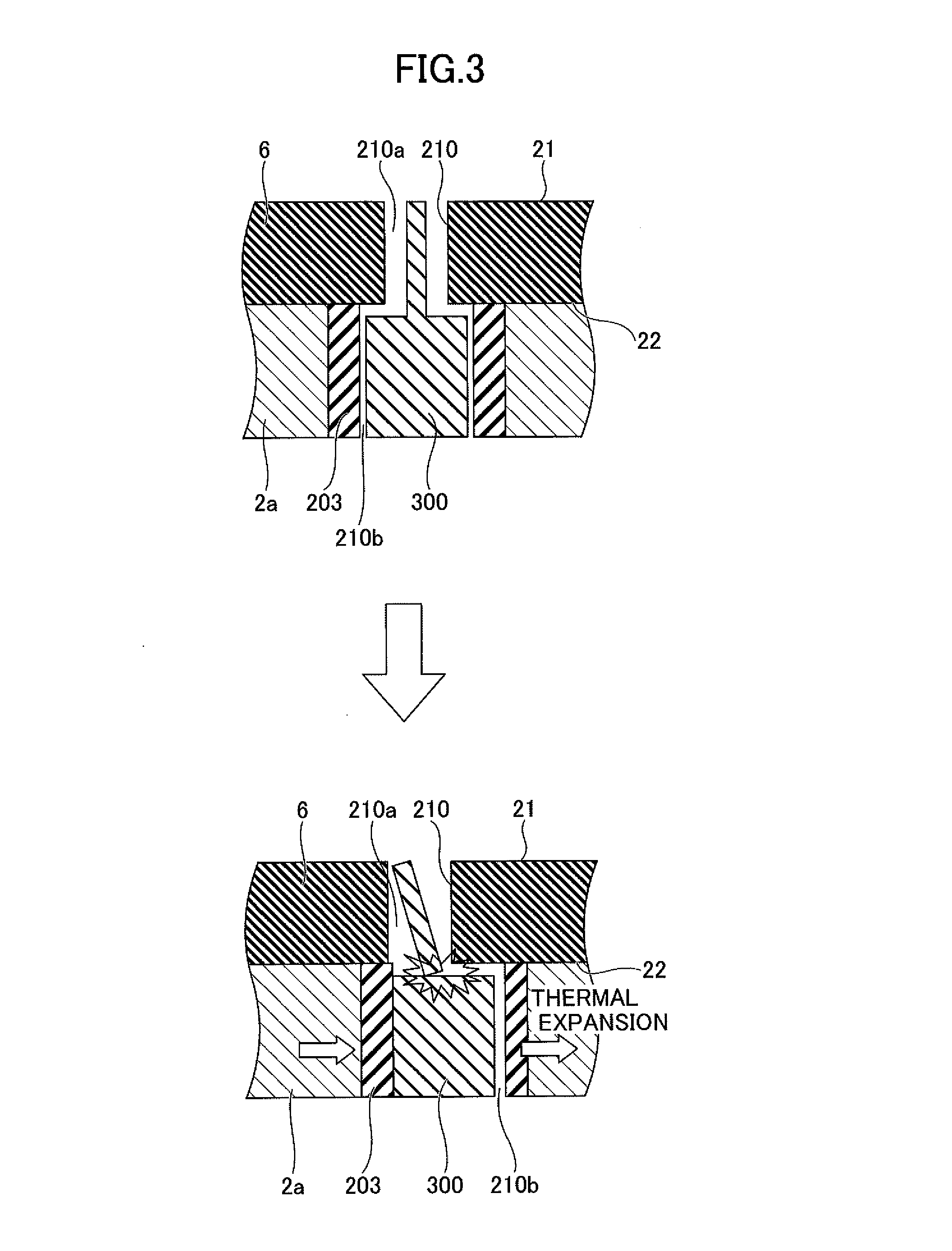
[0007] FIG. 3 illustrates an example of breakage of an embedment member in a comparative example.
[0008] FIG. 4 illustrates an example of an embedment member according to the embodiment of the present invention.
[0009] FIGS. 5A to 5C illustrate an example of a method for manufacturing a mounting stage according to the embodiment of the present invention.
[0010] FIGS. 6A to 6C illustrate a modified example of a first embedment member according to the embodiment of the present invention.
DETAILED DESCRIPTION OF EMBODIMENTS
[0011] Recently, the high-frequency power applied to the mounting stages in plasma processing apparatuses has higher voltages in order to perform plasma processes. In a case where this high-frequency power applied to the mounting stages has higher voltages, the energy of the high-frequency power may concentrate on the hole supplying the heat transfer gas to occasionally cause abnormal electrical discharge. When the abnormal electrical discharge occurs in the hole supplying the heat transfer gas, there is a risk that the quality of the object to be processed processed by the plasma processing apparatus is degraded and a drop of yield occurs.
[0012] An object of the present invention is to provide an embedment member that prevents abnormal electrical discharge in a hole for communicating a heat transfer gas.
[0013] A description of embodiments of the present invention is given below, with reference to the FIG. 1 through FIG. 6.
[0014] The embodiments described below are only examples and the present invention is not limited to the embodiments.
[0015] Through all figures illustrating the embodiments, the same references symbols are used for portions having the same function, and repetitive explanations of these portions are omitted.
[0016] Reference symbols typically designate as follows:
[0017] W: wafer;
[0018] 2: mounting stage;
[0019] 2a: base;
[0020] 6: electrostatic chuck;
[0021] 6c: conductive film;
[0022] 6d: cylindrical member;
[0023] 15: gas supply unit;
[0024] 16: shower head;
[0025] 21: mounting surface;
[0026] 22: back surface;
[0027] 31: heat transfer gas supply unit;
[0028] 100: plasma processing apparatus;
[0029] 210: gas supply pipe;
[0030] 210a: through hole;
[0031] 210b: through hole;
[0032] 219: embedment member;
[0033] 221: first embedment member;
[0034] 221a: step;
[0035] 221b: protrusion;
[0036] 220: second embedment member; and
[0037] 220a: cutout.
[Structure of Plasma Processing Apparatus]
[0038] FIG. 1 illustrates an example of the structure of the plasma processing apparatus 100 of this embodiment. The plasma processing apparatus 100 includes a processing container 1 that is hermetically enclosed and electrically has the ground potential. This processing container 1 is in a cylindrical shape and is made from, for example, aluminum. The processing container 1 separates a space for generating plasma. Inside the processing container 1, the mounting stage 2 is provided to horizontally support a semiconductor wafer (hereinafter, referred to as a "wafer") as an object to be processed (work-piece). The mounting stage 2 includes a base 2a and an electrostatic chuck (ESC) 6. The base 2a is made from conductive metal such as aluminum and has a function as a lower electrode. An electrostatic chuck 6 is made from ceramics such as alumina and has a function of statistically adsorbing the wafer. The mounting stage 2 is supported by a support seat 4. The support seat 4 is supported by a support member 3 made from, for example, quartz. A focus ring 5 made from, for example, silicon is provided in an outer periphery above the mounting stage 2. Further, inside the processing container 1, a cylindrical inner wall member 3a made from, for example, quartz is provided so as to surround the outside of the mounting stage 2 and the support seat 4.
[0039] A first RF power source 10a is connected to the base 2a through the matching box 11a, and a second RF power source 10b is connected to the base 2a through the matching box 11b. The first RF power source 10a supplies high frequency power having a predetermined frequency for generating plasma to the base 2a of the mounting stage 2. The second RF power source 10b supplies high-frequency power having a predetermined frequency lower than that of the first RF power source 10a for drawing ions (for biasing) to the base 2a of the mounting stage 2.
[0040] A shower head having a function as the upper electrode is provided above the mounting stage 2 in parallel with the mounting stage 2. The shower head 16 and the mounting stage 2 function as a pair of electrodes (an upper electrode and a lower electrode).
[0041] The electrostatic chuck 6 is structured by embedding an electrode 6a in an insulator 6b. A direct current power source 12 is connected to the electrode 6a. When a direct voltage is applied from the direct current power source 12 to the electrode 6a to generate coulomb force, the wafer W is adsorbed by the coulomb force.
[0042] A refrigerant flow passage 2d is formed inside the mounting stage 2. A refrigerant inlet pipe 2b and a refrigerant outlet pipe 2c are connected to the refrigerant flow passage 2d. By circulating appropriate refrigerant such as cooling water inside a refrigerant flow passage 2d, the mounting stage 2 is controlled to have a predetermined temperature. A gas supply pipe 210 for supplying a cold and heat transferring gas (hereinafter, referred to as a "heat transfer gas") such as a helium gas is provided on the back surface of the wafer W through the mounting stage 2 or the like. The gas supply pipe a heat transfer gas supply unit 31. By this structure, the wafer W on the mounting stage 2 is controlled to have a predetermined temperature. The internal structure of the gas supply pipe 210 is described later.
[0043] The mounting stage 2 has multiple through holes 200 for multiple (for example, three) pins. Only one through hole is illustrated in FIG. 1. A lifter pin 61 is disposed inside each of the through holes 200. The lifter pin 61 is connected to a drive mechanism 62 so as to be moved up and down by the drive mechanism 62.
[0044] The gas shower head 16 is disposed in a ceiling portion of the processing container 1. The shower head 16 includes a main body 16a and an upper ceiling plate 16b as an electrode plate. The shower head 16 is supported by an upper portion of the processing container 1 via an insulation member 95. The main body 16a is made with aluminum whose surface is subjected to anodic oxidation, for example. The main body attachably and detachably supports a lower portion of the ceiling plate 16b.
[0045] An inside of the main body 16a includes a gas diffusion chamber 16c. A large number of gas communication holes 16d are formed in a bottom portion of the main body 16a so as to be positioned at a lower portion of the main body 16a. Gas introduction holes 16e penetrate the ceiling plate 16b in the thickness direction of the ceiling plate 16b. The gas introduction holes 16e respectively communicate with the above gas communication holes 16d.
[0046] A gas introducing port 16g for introducing a process gas into the gas diffusion chamber 16c is formed in the main body 16a. An end of a gas supply pipe 15a is connected to the gas introducing port 16g. A gas supply unit 15 for supplying a process gas is connected to another end of the gas supply pipe 15a. A mass flow controller (MFC) 15b and an on-off valve V2 are provided in the gas supply pipe 15a sequentially from the upstream side. The process gas is provided for plasma etching and is supplied from the gas supply unit 15 through the gas supply pipe 15a to the gas diffusion chamber 16c. By this structure, the process gas supplied to the gas diffusion chamber 16c is supplied inside the processing container 1 through the gas communication holes 16d and the gas introduction holes 16e.
[0047] A variable direct current power source 72 is electrically connected through a low pass filter (LPF) 71 to the shower head 16 as the above upper electrode. An on-off switch 73 turns on or off supply from the variable direct current power source 72. The electric current, the electric voltage, and on or off of the on-off switch 73 are controlled by the control unit 9. When plasma is generated in a process space by applying radio-frequency waves through the first RF power source 10a and the second RF power source 10b to the mounting stage 2, the control unit 90 turns on the on-off switch 73 so as to cause the shower head 16 to be applied with a predetermined direct voltage where necessary.
[0048] A cylindrical ground conductor 1a is disposed along the sidewall so as to extend over of the height of the shower head 16 in the upward direction. This cylindrical ground conductor 1a has a ceiling in it is upper portion.
[0049] An exhaust port 81 is formed in a bottom portion of the processing container 81. An exhaust device 83 is connected to the exhaust port 81 through an exhaust pipe 82. The exhaust device 83 includes a vacuum pump which is operated to depressurize the inside of the processing container 1 to be a predetermined degree of vacuum. A carry-in and carry-out port 84 for the wafer W is provided in a sidewall inside the processing container 1. A gate valve 85 for opening and closing the carry-in and carry-out port 84 is provided in the carry-in and carry-out port 84.
[0050] A depo-shield 86 is provided along an inner wall surface on a side of the processing container 1. The depo-shield 86 prevents an etching by-product (depo) from attaching to the processing container 1. At a position being substantially the same height as that of the wafer W in this depo-shield 86, a conductive member (a GND block) 89, to which an electric potential relative to the ground is connected so as to be controllable. With this, abnormal electrical discharge is prevented. A depo-shield 87 extends along the inner wall member 3a at a lower end of the depo-shield 86. The depo-shields 86 and 87 are attachable and detachable.
[0051] The operation of the above described plasma processing apparatus 100 is totally controlled by the control unit 90. The control unit 90 includes a CPU 91 controlling various portions of the plasma processing apparatus 100, an interface 92, and a memory 93.
[0052] The interface 92 includes a keyboard, with which a process administrator inputs commands for administering the plasma processing apparatus 100 and a display visualizing an operation state of the plasma processing apparatus 100 and displaying the visualized operation state.
[0053] The memory 93 stores a recipe, in which a control program (software) for implementing various processes performed by a control of the CPU 91, and a recipe storing data for processing conditions or the like are stored. By calling an arbitrary recipe from the memory 93 upon an instruction corresponding to an input operation from the interface 92 where necessary and causing the CPU 91 to execute, a desired process is performed by the plasma processing apparatus 100 under the control by the CPU 91. The control program and the recipe storing the data for processing conditions or the like can be used from a computer recording medium (for example, a hard disk, a CD, a flexible disk, a semiconductor memory, or the like) readable by the computer or can be used online through, for example, a dedicated line continuously transmitting the control program and the recipe.
[Structure of Mounting Stage]
[0054] Referring to FIG. 2, an example of the structure of the mounting stage 2 is described. FIG. 2 is a cross-sectional view schematically illustrating a mounting stage according to the embodiment of the present invention. The mounting stage 2 includes a base 2a and an electrostatic chuck 6. In the mounting stage 2, the electrostatic chuck 6 is shaped like a disk. The electrostatic chuck 6 has a mounting surface for mounting the wafer W similarly shaped like a disk and a back surface 22 facing the mounting surface 21. The base 2a is joined to the back surface 22 of the electrostatic chuck 6.
[0055] An end of the gas supply pipe 210 (a gas port) is formed on the mounting surface 21. The gas supply pipe 210 is formed with the through holes 210a and 210b and supplies a heat transfer gas such as a helium gas to the back surface of the wafer W. The through hole 210a is provided so as to penetrate from the back surface 22 of the electrostatic chuck 6 to the mounting surface 21. Said differently, the inner wall of the through hole 210a is formed by the electrostatic chuck 6. The through hole 210b is formed to penetrate through the back surface of the base 2a to a joint face between the base 2a and the electrostatic chuck 6. Said differently, the inner wall of the through hole 210b is formed by the base 2a.
[0056] The through hole 210a is an example of a first hole penetrating through the mounting surface 21 on which the wafer W is mounted and the back surface 22 opposite to the mounting surface 21. The through hole 210b is an example of a second hole formed in the base 2a and communicating with the first hole. The electrostatic chuck 6 is an example of a plate-like portion in which the first hole is formed. However, the plate-like portion, in which the first hole is formed, may not have the function of the electrostatic chuck 6.
[0057] The through hole 210a has a step. The inner diameter of the through hole above the step is smaller than the inner diameter of the through hole below the step. The inner diameter of the through hole 210b is equal to the the inner diameter of the through hole below the step. The through hole 210a and the through hole 210b are formed so as to be positionally aligned at, for example, a normal temperature. A gas sleeve made of alumina is provided in the gas supply pipe 210. A spacer may be provided on an inner wall of the gas supply pipe 210.
[Embedment Member]
[0058] An embedment member 219 is disposed inside the gas supply pipe 210. Specifically, a first embedment member 221 and a second embedment member 220 are respectively disposed inside the through hole 210a and the through hole 210b.
[0059] The thickness of the first embedment member 221 is the same as the thickness of the electrostatic chuck 6. The thickness of the first embedment member 221 may be thinner than the thickness of the electrostatic chuck 6. A step 221a is formed in the first embedment member 221. The outer diameter of the first embedment member 221 above the step 221a is smaller than the outer diameter of the first embedment member 221 below the step 221a. The longitudinal cross-sectional view of the first embedment member 221 is shaped like a protrusion.
[0060] The first embedment member 221 is formed by a material having plasma durability such as ceramics. For example, the first embedment member 221 may be made of any one of quartz, silicon carbide, silicon nitride, aluminum oxide, aluminum nitride, yttria, titanium oxide, and tungsten carbide. The first embedment member 221 is formed by a material having plasma durability such as ceramics. For example, the material having low plasma durability may be replaced by silicon, tungsten, titanium, silicone, Teflon ("Teflon" is a registered trademark), elastomer, or fluorine resin.
[0061] The second embedment member 220 is disposed below the first embedment member 221. The second embedment member 220 is made of, for example, alumina. A cutout 220a is formed in a peripheral edge of the upper end portion of the second embedment member 220. The cutout 220a is an example of a recess formed in the peripheral edge of the upper end portion of the second embedment member 220.
[0062] The outer diameter of the first embedment member 221 is smaller than the inner diameter of the through hole 210a. The outer diameter of the second embedment member 220 is smaller than the inner diameter of the through hole 210b. Therefore, the the first embedment member 221 and the second embedment member 220 are arranged to keep a predetermined interval from the inner wall of the gas supply pipe 210 to provide a heat transfer gas path inside the through holes 210a and 210b.
[0063] Further, in a case where the the first embedment member 221 is horizontally misaligned with the second embedment member 220, the cutout 220a in the upper end of the second embedment member 220 maintains the heat transfer gas path to enable the heat transfer gas to be sufficiently flown. However, when the width of the cutout 220a is unnecessarily large, there is a risk of generating abnormal electrical discharge. Therefore, the width of the cutout 220a is sufficient to enable the heat transfer gas to flow in the case where the first embedment member 221 and the second embedment member 220 are horizontally misaligned. Further, the cutout 220a may be formed through the entire periphery or shaped in a crescentic shape or a sector shape.
[0064] The high-frequency power applied to the mounting stage 2 in the plasma processing apparatus 100 has a higher voltage. When the high-frequency power applied to the mounting stage 2 has the higher voltage, abnormal electrical discharge may be generated near the through hole 210a.
[0065] Said differently, in the plasma processing apparatus 100, when the high-frequency power is applied to the mounting stage 2, an electric potential difference occurs between the wafer W and the back surface 22 of the electrostatic chuck 6 due to an electrostatic capacity of the electrostatic chuck 6. With this, if the electric potential difference of an RF electric potential generated in the through hole 210a exceeds a limit value, at which discharge is generated, abnormal electrical discharge occurs.
[0066] Meanwhile, it is experientially known that the abnormal electrical discharge is prevented from generating by shortening a straight travelling distance of charged particle of the heat transfer gas inside the through hole 210a. Within the embodiment, the embedment member 219 is disposed inside the gas supply pipe 210 to prevent the abnormal electrical discharge from occurring. Hereinafter, problems in the structure of comparative example are described, the structure of the embedment member 219 of the embodiment is described.
[Breakage of Embedment Member in Comparative Example]
[0067] Referring to FIG. 3, an example of breakage in the embedment member 300 of the comparative example is described. The embedment member 300 of the comparative example is arranged by providing a predetermined interval from the inner wall of the gas supply pipe 210.
[0068] The abnormal electrical discharge in the through hole 210a can be prevented by reducing the interval between the embedment member 300 and the through hole 210a. The abnormal electrical discharge in the through hole 210a can also be prevented by shortening the linear portion of the heat transfer gas path. This is because the energy of electrons in the heat transfer gas can be reduced. Then, as illustrated in the upper half of FIG. 3, the inner diameter of the through hole 210b is made greater than the inner diameter of the through hole 210a, and a portion of the embedment member 300 corresponding to the through hole 210b is made wider.
[0069] However, there may be a case where the embedment member 300 is broken. In a case where the plasma process is performed, the temperature of the mounting stage 2 become high, for example, 100.degree. C. to 200.degree. C. The electrostatic chuck 6 is made of ceramics and the base 2a is made of metal. The electrostatic chuck 6 and the base 2a have different thermal expansion coefficients. Therefore, if the temperature of the electrostatic chuck 6 and the base 2a become high, the through holes 210a and 210b are misaligned as illustrated in the lower half of FIG. 3 due to differential thermal expansion between the electrostatic chuck 6 and the base 2a. In this case, the shear stress is applied to the embedment member 300 from the base 2a. As a result, there may occur a case where a part corresponding to the through hole 210a of the embedment member 300 contacts the electrostatic chuck 6 and the embedment member 300 breaks.
[Embedment Member of this Embodiment]
(Prevention of Breakage of Embedment Member)
[0070] As illustrated in the upper half of FIG. 4, the embedment member 219 of the embodiment is structured such that the first embedment member 221 disposed on the second embedment member 220 is not fixed to the second embedment member 220 to prevent breakage by the thermal expansion. With this structure, as illustrated in the lower half of FIG. 4, in a case where the positions of the through holes 210a and 210b are misaligned due to the thermal expansion, shear stress is applied to the embedment member 219 from the base 2a. In this case, according to the embodiment, the embedment member 219 is prevented from being broken because the second embedment member 220 is misaligned relative to the first embedment member 221.
[0071] The cutout 220a of the second embedment member 220 maintains the heat transfer gas path inside the gas supply pipe 210 even if the first embedment member 221 and the second embedment member 220 are misaligned. With this, it is possible to sufficiently supply the heat transfer gas to the back surface of the wafer W.
(Prevention of Spread of Embedment Member)
[0072] When the inside of the processing container 1 is evacuated to vacuum by the exhaust device 83, the inside of the gas supply pipe 210 having the embedment member 219 is also evacuated onto a side of a process space. If the wafer W is not mounted on the electrostatic chuck 6 at that time, because the first embedment member 221 is not fixed to the second embedment member 220, there a risk that the first embedment member 221 flies out through the hole 210a into the process space above the electrostatic chuck 6.
[0073] The first embedment member 221 includes a step 221a. The outer diameter below the step 221a is greater than the outer diameter above the step 221a. With this, it is possible to prevent the first embedment member 221 from spreading inside the process space in a case where the inside of the processing container 1 is evacuated to vacuum or the heat transfer gas is supplied to the back surface of the wafer W.
[0074] The first embedment member 221 is not limited to the protrusion-like shape, and may be in a shape such that a portion wider than that in the upper end portion of the first embedment member 221 on a lower side. According to such a shape, the first embedment member 221 can be prevented from flying out of the gas supply pipe 210.
[Manufacturing Method of Mounting Stage]
[0075] Next, referring to FIGS. 5A to 5C, an example of the manufacturing method of the embodiment is described. FIGS. 5A to 5C illustrate examples of the manufacturing method for manufacturing the mounting stage 2 of this embodiment. According to the manufacturing method, as illustrated in FIG. 5A, the gas supply pipe 210 penetrating through the mounting stage 2 is formed after registering the positions of the through hole 210a penetrating the electrostatic chuck 6 and the through hole 210b penetrating through the base 2a. The number of the gas supply pipes 210 provided at predetermined positions of the mounting stage 2 is about 12 to 18 pieces. The through hole 210b is formed by disposing a sleeve for gas 203 made of alumina.
[0076] Within the embodiment, a rod-like protrusion 221b protruding on a lower side is formed at the lower end portion of the first embedment member 221. The embedment member 219 formed by fitting the protrusion 221b into a recess formed at the upper end of the second embedment member 220 is prepared. The first embedment member 22 of this embodiment is separate from the second embedment member 220. Therefore, according to this manufacturing method of the embedment member 219, the protrusion 221b formed at the lower end of the first embedment member 221 is used to register the first embedment member 221 and the second embedment member 220 so that center lines o of the first embedment member 221 and the second embedment member 220 match.
[0077] Next, as illustrated in FIG. 5B, the embedment member 219 is inserted in the through hole 210a and the through hole 210b. The embedment member 219 is disposed inside the gas supply pipe 210 so that a predetermined space as the heat transfer gas path is formed between embedment member 219 and the through hole 210a and 210b. With this, the first embedment member 221 is disposed inside the through hole 210a and the second embedment member 220 is disposed inside the through hole 210b.
[0078] As described, the temperature of the mounting stage 2 is high such as 100.degree. C. to 200.degree. C. When the temperature of the mounting stage 2 becomes high, the positions of the through hole 210a and the through hole 210b are misaligned due to a differential thermal coefficient between the electrostatic chuck 6 and the base 2a.
[0079] In this case, when shear stress is applied to the embedment member 219 from the base 2a, the second embedment member 220 is misaligned from the first embedment member 221 so that the protrusion 221b is divided from the first embedment member 221. As a result, as illustrated in FIG. 5C, the first embedment member 221 and the second embedment member 220 are not mutually fixed. With this structure, according to the manufacturing method of the mounting stage 2 of the embodiment, the mounting stage 2 can be manufactures so that the embedment member 219 does not break due to the misalignment of the positions of the through hole 210a and the through hole 210b.
[0080] Although, according to this manufacturing method, the example where the protrusion 221b is divided from the first embedment member 221 is described, the embodiment is not limited thereto. For example, the protrusion 221b may not be divided from the first embedment member 221. The protrusion 221b may be made of soft material such as a resin so as to deform depending on the misalignment of the positions of the through holes 210a and 210b. With this, the mounting stage 2 may be manufactured so that the embedment member 219 does not break.
[0081] Further, it is sufficient that the protrusion 221b can register the first embedment member 221 and the second embedment member 220 and can provisionally fix at the time of manufacture. One or multiple protrusions may be provided at any position on the lower surface of the first embedment member 221. Furthermore, the protrusion 221b is not limited to a rod-like shape but a screw-like shape.
[Modified Example]
[0082] Finally, referring to FIGS. 6A to 6C, a modified example of the first embedment member 221 is described. FIGS. 6A thru 6C illustrate a modified example of a first embedment member 221 according to the embodiment of the present invention. The first embedment member is in any one of a shape of a protrusion, a shape where a width of a portion increases as the portion approaches a lower end, a shape where a portion having a widest width is positioned between an upper end and the lower end, and a shape where a portion having a narrowest width is positioned between the upper end and the lower end (a shape of a gourd whose upper end and lower end are flat).
[0083] FIG. 6A illustrates an example of a shape where the width of a portion increases as the portion approaches the lower end. The shape of the first embedment member 221 is a conic shape, and a longitudinal cross-sectional view of the first embedment member 221 is substantially a triangle (the upper end is flat).
[0084] FIG. 6B illustrates an example of a shape where a portion having the widest width is positioned between the upper end and the lower end. The shape of the longitudinal cross-sectional view of the first embedment member 221 is substantially a rhombus (the upper and lower ends are flat).
[0085] FIG. 6C illustrates an example of a shape where a portion having a dent is positioned between the upper end and the lower end. The shape of the longitudinal cross-sectional view of the first embedment member 221 is substantially a gourd.
[0086] Referring to FIGS. 6A to 6C, the examples of the first embedment member 221 are in the shape where the portion having the widest width is positioned between the upper end and the lower end. The shape of the first embedment member 221 is not limited as long as the portion having a width wider than the width of the upper end on a side lower than the upper end.
[0087] The plasma processing apparatus 100 may be a plasma processing apparatus having the mounting stage 2 manufactured by the manufacturing method illustrated in FIG. 5. According to the manufacturing method for manufacturing the plasma processing apparatus 100 and the mounting stage 2, the first embedment member 221 does not fly apart and the embedment member 219 can be prevented from breaking.
[0088] Further, by disposing the embedment member 219 inside the gas supply pipe 210, the heat transfer gas is sufficiently supplied to the back surface of the wafer W, and simultaneously it is possible to prevent abnormal electrical discharge from occurring in the through hole 210a by electric power of a high frequency applied to the base 2a.
[0089] The plasma processing apparatus of the embodiments may be any type of Capacitively Coupled Plasma (CCP), Inductively Coupled Plasma (ICP), Radial Line Slot Antenna, Electron Cyclotron Resonance Plasma (ECR), and Helicon Wave Plasma (HWP).
[0090] Within the embodiment, the wafer W is mentioned as an example of an object to be processed by the plasma processing apparatus. However, the object to be processed is not limited to this and may be various substrates used for a Liquid Crystal Display (LCD) and a Flat Panel Display (FPD), a Compact Disk (CD) substrate, a printed wiring board, and so on.
[0091] According to the embodiment, it is possible to provide an embedment member which can prevent abnormal electrical discharge from occurring in the hole of the heat transfer gas.
[0092] All examples and conditional language recited herein are intended for pedagogical purposes to aid the reader in understanding the invention embodiments and the concepts contributed by the inventor to furthering the art, and are to be construed as being without limitation to such specifically recited examples and conditions, nor does the organization of such examples in the specification relate to a showing of superiority or inferiority of the invention embodiments. Although the method for manufacturing the plasma processing apparatus and the mounting stage of the present invention have been described in detail, it should be understood that the various changes, substitutions, and alterations could be made hereto without departing from the spirit and scope of the invention.
* * * * *
D00000
D00001
D00002
D00003
D00004
D00005
D00006
XML
uspto.report is an independent third-party trademark research tool that is not affiliated, endorsed, or sponsored by the United States Patent and Trademark Office (USPTO) or any other governmental organization. The information provided by uspto.report is based on publicly available data at the time of writing and is intended for informational purposes only.
While we strive to provide accurate and up-to-date information, we do not guarantee the accuracy, completeness, reliability, or suitability of the information displayed on this site. The use of this site is at your own risk. Any reliance you place on such information is therefore strictly at your own risk.
All official trademark data, including owner information, should be verified by visiting the official USPTO website at www.uspto.gov. This site is not intended to replace professional legal advice and should not be used as a substitute for consulting with a legal professional who is knowledgeable about trademark law.