Method Of Spacer-defined Direct Patterning In Semiconductor Fabrication
Nozawa; Toshihisa ; et al.
U.S. patent application number 15/900425 was filed with the patent office on 2019-08-22 for method of spacer-defined direct patterning in semiconductor fabrication. The applicant listed for this patent is ASM IP Holding B.V.. Invention is credited to Dai Ishikawa, Tomohiro Kubota, Toshihisa Nozawa.
| Application Number | 20190259612 15/900425 |
| Document ID | / |
| Family ID | 67616998 |
| Filed Date | 2019-08-22 |


View All Diagrams
| United States Patent Application | 20190259612 |
| Kind Code | A1 |
| Nozawa; Toshihisa ; et al. | August 22, 2019 |
METHOD OF SPACER-DEFINED DIRECT PATTERNING IN SEMICONDUCTOR FABRICATION
Abstract
A method of spacer-defined direct patterning in semiconductor fabrication includes: providing a photoresist structure having a target width of lines; trimming the photoresist structures such that a width of each trimmed photoresist structure is smaller than the target width; depositing an oxide film on the template, thereby entirely covering with the oxide film an exposed top surface of the template and the trimmed photoresist structures; etching the oxide film-covered template to remove an unwanted portion of the oxide film without removing the trimmed photoresist structures so as to form vertical spacers isolated from each other, each spacer substantially maintaining the target width and being constituted by the trimmed photoresist structures and a vertical portion of the oxide film covering sidewalls of the trimmed photoresist structures; and etching the spacer-formed template to transfer a pattern constituted by the spacers to the template.
| Inventors: | Nozawa; Toshihisa; (Kawasaki-shi, JP) ; Ishikawa; Dai; (Tokyo, JP) ; Kubota; Tomohiro; (Tokyo, JP) | ||||||||||
| Applicant: |
|
||||||||||
|---|---|---|---|---|---|---|---|---|---|---|---|
| Family ID: | 67616998 | ||||||||||
| Appl. No.: | 15/900425 | ||||||||||
| Filed: | February 20, 2018 |
| Current U.S. Class: | 1/1 |
| Current CPC Class: | H01L 21/31116 20130101; H01L 21/76832 20130101; H01L 21/32137 20130101; H01L 21/02164 20130101; H01L 21/0338 20130101; H01L 21/0228 20130101; H01L 21/0332 20130101; H01L 21/0337 20130101; H01L 21/02274 20130101; H01L 21/02219 20130101; H01L 21/027 20130101; H01L 21/0276 20130101; H01L 21/0275 20130101; H01L 21/31144 20130101; H01L 21/0273 20130101; H01L 21/76816 20130101; H01L 21/31138 20130101 |
| International Class: | H01L 21/033 20060101 H01L021/033; H01L 21/311 20060101 H01L021/311; H01L 21/027 20060101 H01L021/027; H01L 21/02 20060101 H01L021/02 |
Claims
1. A method of spacer-defined direct patterning in semiconductor fabrication, comprising: (i) presetting a target width of lines to be patterned in a template using photoresist structures formed by photolithography on the template; (ii) providing the template having the photoresist structures patterned thereon; (iii) trimming the photoresist structures such that a width of each trimmed photoresist structure is smaller than the target width; (iv) depositing an oxide film on the template, thereby entirely covering with the oxide film an exposed top surface of the template and the trimmed photoresist structures; (v) etching the oxide film-covered template to remove an unwanted portion of the oxide film without removing the trimmed photoresist structures so as to form vertical spacers isolated from each other, each spacer substantially maintaining the target width and being constituted by the trimmed photoresist structures and a vertical portion of the oxide film covering sidewalls of the trimmed photoresist structures; and (vi) etching the spacer-formed template to transfer a pattern constituted by the spacers to the template.
2. The method according to claim 1, wherein the photoresist structures in step (ii) have a width substantially the same as the target width.
3. The method according to claim 1, wherein the oxide film deposited in step (iv) has a thickness such that each oxide film-covered trimmed photoresist structure has a width substantially the same as the target width.
4. The method according to claim 1, wherein in step (iv), the oxide film is a conformal film deposited by plasma-enhanced atomic layer deposition (PEALD).
5. The method according to claim 1, wherein in step (iv), the oxide film is deposited by plasma-enhanced atomic layer deposition (PEALD) wherein pressure, temperature, and/or RF power are/is controlled so that a dry etch rate of a portion of the oxide film deposited on a top surface of each trimmed photoresist structure is higher than that of a portion of the oxide film deposited on sidewalls of each trimmed photoresist structure.
6. The method according to claim 1, wherein each photoresist structure is trimmed in step (iii) so as to reduce its width by 1 nm to 5 nm on each side of the photoresist structure.
7. The method according to claim 1, wherein the photoresist structures are formed on an anti-reflective layer of the template, and in step (v), when the unwanted portion of the oxide film is removed, a portion of the anti-reflective layer formed underneath the unwanted portion of the oxide film is also removed.
8. The method according to claim 1, wherein in step (i), the preset target width is in the range of 10 nm to 20 nm.
9. The method according to claim 1, wherein step (ii) comprises forming the photoresist structures by photolithography using EUV (Extrema Ultra Violet) light.
10. The method according to claim 1, further comprising, prior to step(iii): (iia) depositing by plasma-enhanced atomic layer deposition (PEALD) a thin oxide film having a thickness of about 2 nm or less on the template, thereby entirely covering with the thin oxide film an exposed top surface of the template and the photoresist structures.
11. The method according to claim 10, wherein the trimming in step (iii) is conducted by direct plasma etching.
12. The method according to claim 10, wherein the thin oxide film in step (iia) and the oxide film in step (iv) are constituted by a same material.
13. The method according to claim 10, wherein the photoresist structures in step (ii) are constituted by sparely and densely arranged photoresist structures having different line spaces.
14. The method according to claim 10, wherein the thin oxide film in step (iia) is constituted by SiO.sub.2, TiO, HfO, or AlO.
15. The method according to claim 1, wherein the photoresist structures have an LER (Line-Edge Roughness) of more than 3.5 nm, and an LWR (Line-Width Roughness) of more than 5 nm prior to step (iii).
16. The method according to claim 15, wherein the trimmed photoresist structures have an LER of less than 3.5 nm, and an LWR of less than 5 nm prior to step (iv).
17. The method according to claim 16, wherein the oxide film-covered trimmed photoresist structures have an LER of 3 nm or less, and an LWR of 4 nm or less prior to step (v).
18. The method according to claim 1, wherein a reactant gas used in step (iii) comprises no oxygen.
19. The method according claim 1, wherein steps (ii) to (v) are conducted at a temperature of 150.degree. C. or lower.
20. The method according to claim 1, wherein steps (ii) to (iv) are continuously conducted in a same reaction chamber.
Description
BACKGROUND OF THE INVENTION
Field of the Invention
[0001] The present invention generally relates to a method of patterning in semiconductor fabrication, particularly a method of spacer-defined direct patterning in semiconductor fabrication using, e.g., EUV (Extreme Ultra Violet) for photolithography.
Description of the Related Art
[0002] To correspond to miniaturization of semiconductor devices, a reduction of wavelength of light source for photolithography progresses, e.g., changing from ArF (Argon Fluoride laser) to EUV. Heretofore, due to low productivity of EUV lithography as discussed below, miniaturization of semiconductor devices has been achieved by using spacer-defined double patterning (SDDP). However, there is a limit of miniaturization by SDDP due to limited exposure accuracy, and also, the prospect of actually using EUV lithography has recently emerged. Accordingly, it is expected that direct patterning using EUV lithography will be placed into practical use in semiconductor fabrication in the future.
[0003] EUV lithography enables patterning with a pattern dimension of 10 to 20 nm (the minimum dimension in ArF laser lithography is approximately 40 nm); however, patterning accuracy, which is surface roughness evaluated by LER (Line-Edge Roughness) and LWR (Line-Width Roughness), depends on the characteristics of polymer constituting a resist, and thus, a surface roughness of approximately 5 nm may be the lower limit and has not yet improved. Thus, in fine wiring for microfabrication, undulation or waviness of fine wiring having a width of 5 nm is inevitable and causes line-to-line short circuits. The present inventors have conducted research to improve patterning accuracy in semiconductor fabrication.
[0004] Any discussion of problems and solutions in relation to the related art has been included in this disclosure solely for the purposes of providing a context for the present invention, and should not be taken as an admission that any or all of the discussion was known at the time the invention was made.
SUMMARY OF THE INVENTION
[0005] In some embodiments, variations in microfabrication can be reduced by providing a template having a resist patterned by EUV lithography; conducting trimming or etching of the resist using a plasma-enhanced atomic layer deposition (PEALD) apparatus; and depositing a SiO.sub.2 film on an exposed surface of the template including the trimmed resist at a thickness such that the dimensions of the pre-trimmed resist are resumed so as to cover the trimmed resist having rough surfaces while substantially maintaining the original dimensions of the resist.
[0006] For purposes of summarizing aspects of the invention and the advantages achieved over the related art, certain objects and advantages of the invention are described in this disclosure. Of course, it is to be understood that not necessarily all such objects or advantages may be achieved in accordance with any particular embodiment of the invention. Thus, for example, those skilled in the art will recognize that the invention may be embodied or carried out in a manner that achieves or optimizes one advantage or group of advantages as taught herein without necessarily achieving other objects or advantages as may be taught or suggested herein.
[0007] Further aspects, features and advantages of this invention will become apparent from the detailed description which follows.
BRIEF DESCRIPTION OF THE DRAWINGS
[0008] These and other features of this invention will now be described with reference to the drawings of preferred embodiments which are intended to illustrate and not to limit the invention. The drawings are greatly simplified for illustrative purposes and are not necessarily to scale.
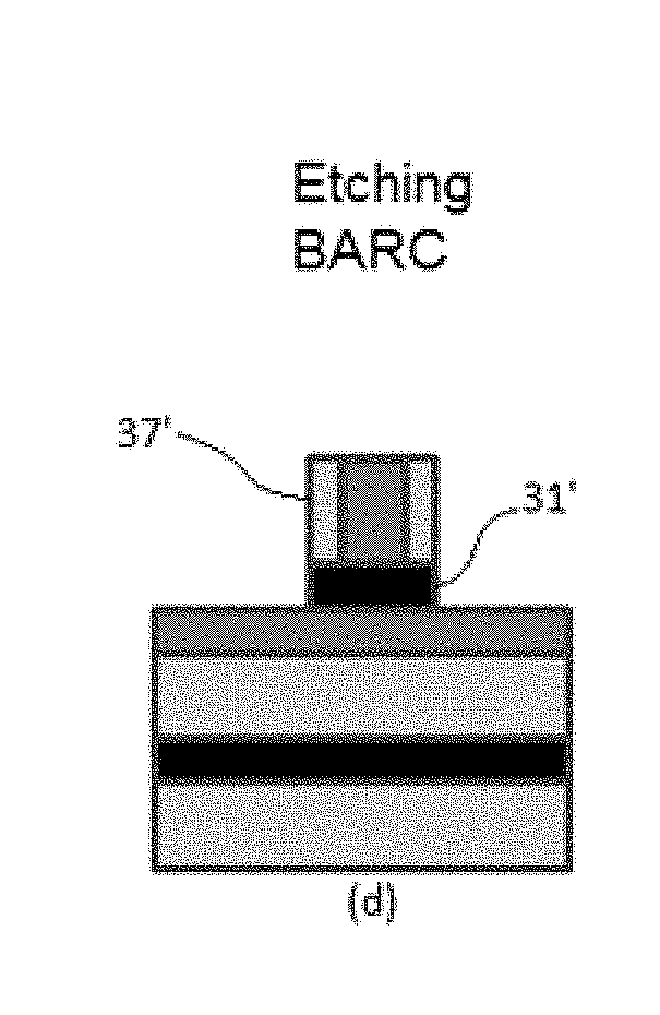
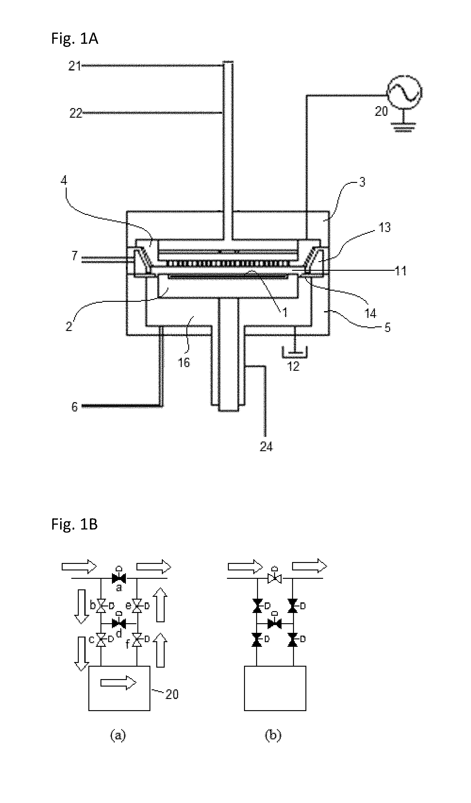
[0009] FIG. 1A is a schematic representation of a PEALD (plasma-enhanced atomic layer deposition) apparatus for depositing a dielectric film usable in an embodiment of the present invention.
[0010] FIG. 1B illustrates a schematic representation of a precursor supply system using a flow-pass system (FPS) usable in an embodiment of the present invention.
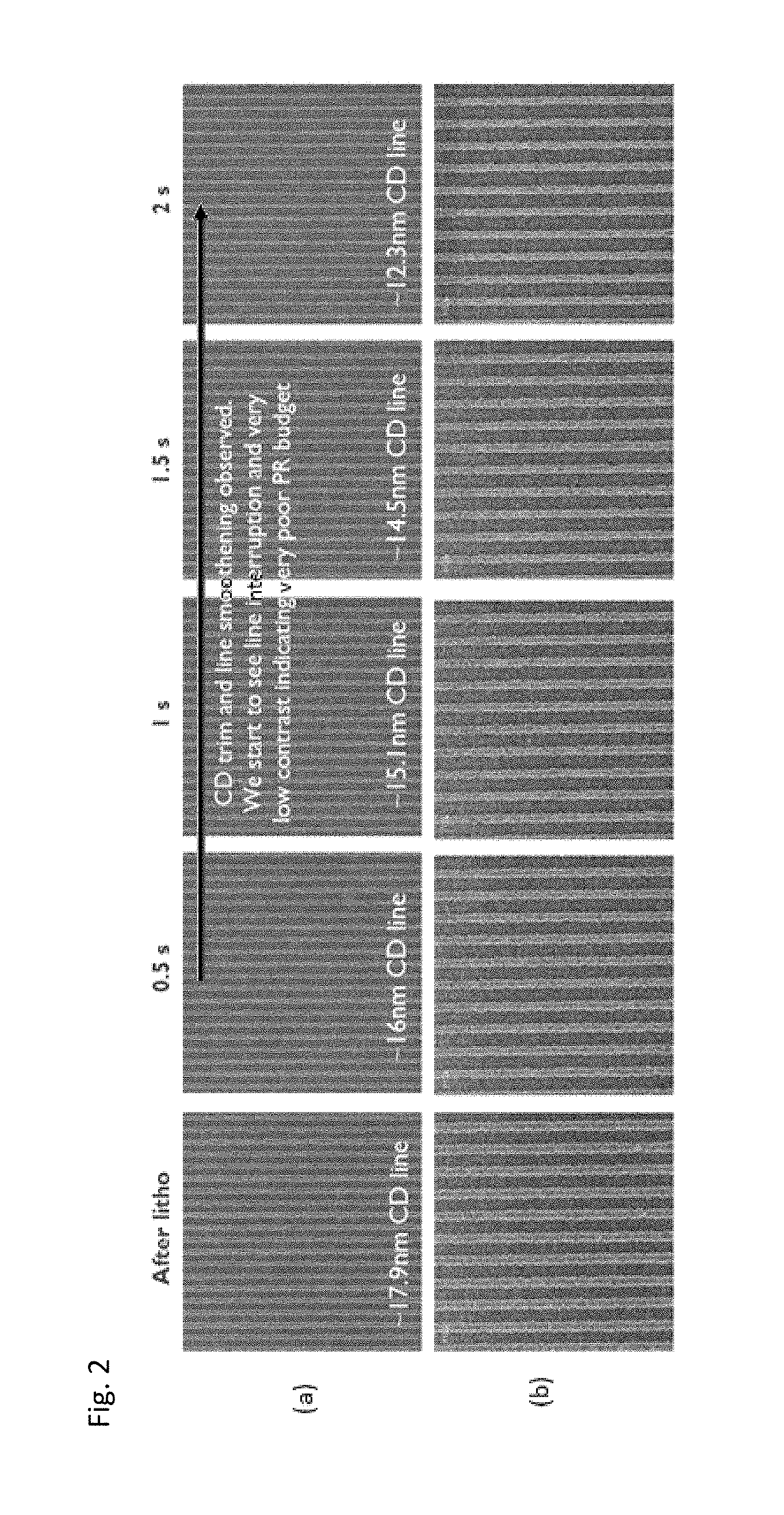
[0011] FIG. 2 shows STEM photographs of patterned surfaces after EUV lithography without trimming ("After litho"), after 0.5 seconds of trimming ("0.5 s"), after 1.0 seconds of trimming ("1 s"), after 1.5 seconds of trimming ("1.5 s"), and after 2.0 seconds of trimming ("2 s"), wherein lower photos (b) are taken at a higher magnification than that for upper photos (a).
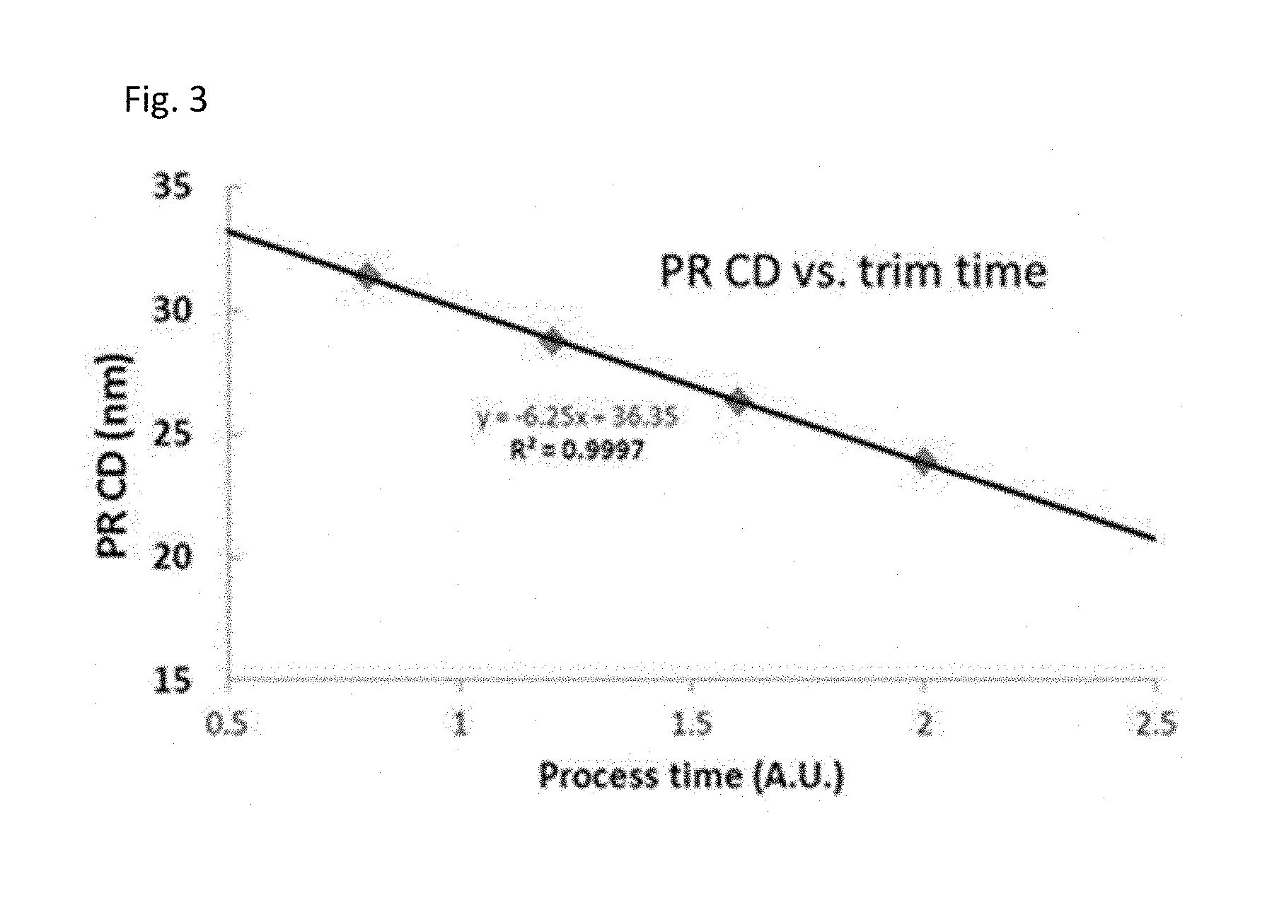
[0012] FIG. 3 is a graph showing the relationship between CD of a photoresist ("PR CD") and process times of trimming ("Process time") according to an embodiment of the present invention.
[0013] FIG. 4 shows a schematic representation of pattern transfer (steps (a) to (f)) using spacer-defined double patterning (SDDP) and a schematic representation of pattern transfer (steps (a'), (b'), and (f')) using spacer-defined direct patterning.
[0014] FIG. 5 shows a schematic representation of pattern transfer (steps (a) to (e)) using spacer-defined direct patterning according to an embodiment of the present invention.
[0015] FIG. 6 shows a schematic representation of pattern transfer (steps (a) to (e), additionally step (a')) using spacer-defined direct patterning according to another embodiment of the present invention.
[0016] FIG. 7 shows STEM photographs of patterned lines of a photoresist formed by photolithography ("AFTER LITHO" in (a)) and after deposition of an oxide film ("PEALD-SIO2 SPACER DEPOSITION" in (b)) according to an embodiment of the present invention.
[0017] FIG. 8 shows STEM photographs of patterned lines of a photoresist formed by photolithography ("After litho"), after 9 seconds of trimming ("After 9s trim"), and after deposition of an oxide film ("After spacer dep") according to an embodiment of the present invention. FIG. 8 also shows CD, LWR, and LER thereof.
[0018] FIG. 9 is a graph showing the relationship between LER and LWR of a photoresist ("LER/LWR") and process times of trimming ("Trim time") according to an embodiment of the present invention.
[0019] FIG. 10 is a table showing CD corresponding to the measuring points shown in FIG. 9.
[0020] FIG. 11 shows STEM photographs of cross-sectional views of patterned lines of a photoresist formed by photolithography ("initial" in (a)) and after depositing a SiO layer by ALD thereon ("SiO ALD (.about.2 nm)" in (b)) according to an embodiment of the present invention.
[0021] FIG. 12 shows STEM photographs of cross-sectional views of patterned lines after depositing the SiO layer by ALD shown in (b) of FIG. 11 ("SiO ALD (.about.2 nm)" in (b)), after trimming the patterned lines for 10 seconds ("ALD+trim(10 s)" in (c)), after trimming the patterned lines for 15 seconds ("ALD+trim(15 s)" in (d)), and after trimming the patterned lines for 20 seconds ("ALD+trim(20 s)" in (e)) according to an embodiment of the present invention.
[0022] FIG. 13 is a graph showing changes in height and CD (nm) of the patterned lines when the trimming time changed according to the embodiment shown in FIG. 12.
[0023] FIG. 14 is a graph showing changes in height, width (nm), and LWR (nm) of patterned lines when the trimming time changed according to an embodiment of the present invention.
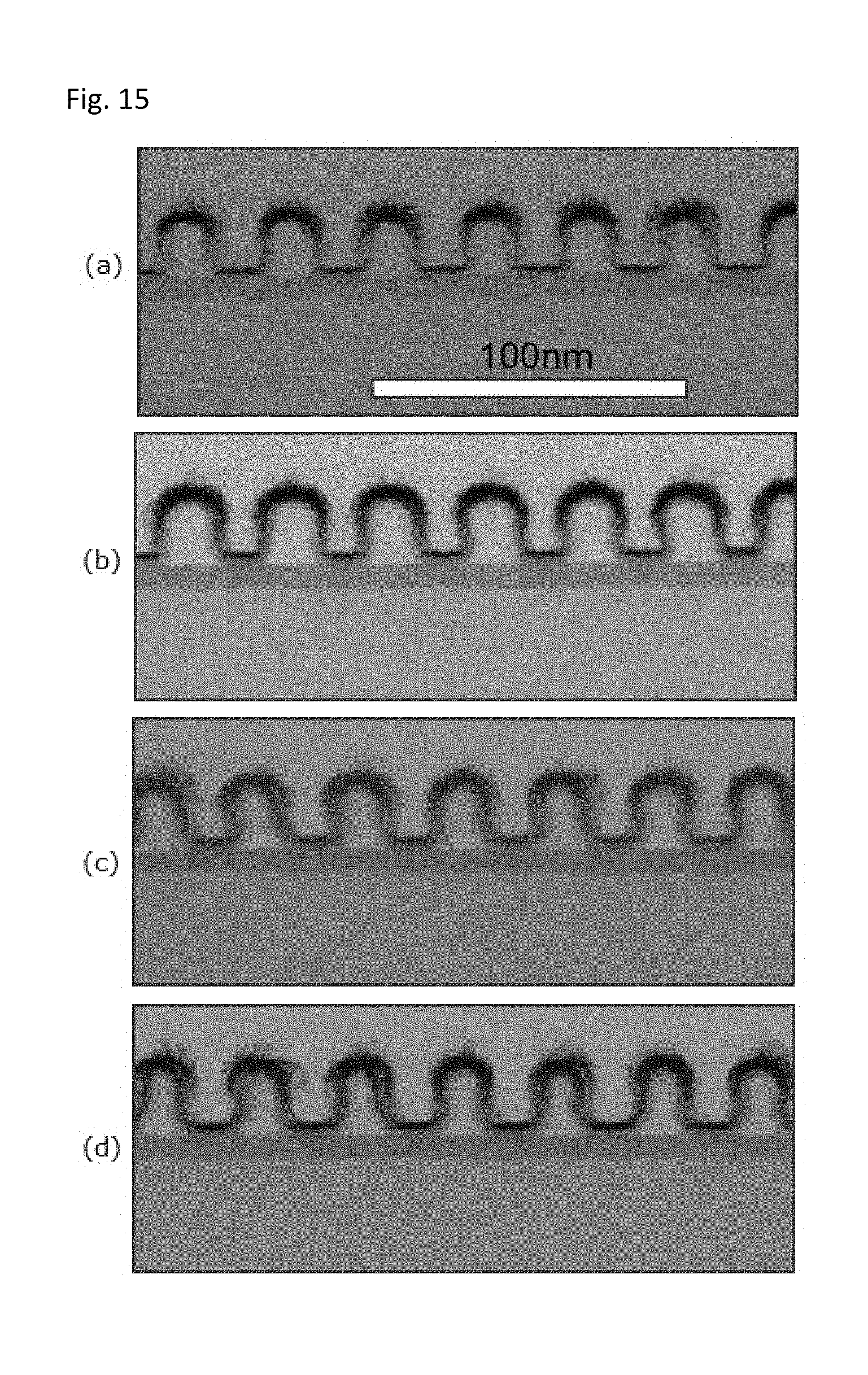
[0024] FIG. 15 shows STEM photographs of cross-sectional views of patterned lines before depositing the SiO layer by ALD in (a) corresponding to "initial" in FIG. 14, after depositing the SiO layer by ALD in (b) corresponding to "Deposition" in FIG. 14, after trimming the patterned lines for 10 seconds in (c) corresponding to "Deposition+Trimming (10 s)" in FIG. 14, and after trimming the patterned lines for 15 seconds in (d) corresponding to "Deposition+Trimming (15 s)" in FIG. 14.
DETAILED DESCRIPTION OF EMBODIMENTS
[0025] In this disclosure, "gas" may include vaporized solid and/or liquid and may be constituted by a single gas or a mixture of gases, depending on the context. Likewise, an article "a" or "an" refers to a species or a genus including multiple species, depending on the context. In this disclosure, a process gas introduced to a reaction chamber through a showerhead may be comprised of, consist essentially of, or consist of a silicon-containing precursor and an additive gas. The additive gas may include a reactant gas for nitriding and/or carbonizing the precursor, and an inert gas (e.g., noble gas) for exciting the precursor, when RF power is applied to the additive gas. The inert gas may be fed to a reaction chamber as a carrier gas and/or a dilution gas. Further, in some embodiments, no reactant gas is used, and only noble gas (as a carrier gas and/or a dilution gas) is used. The precursor and the additive gas can be introduced as a mixed gas or separately to a reaction space. The precursor can be introduced with a carrier gas such as a rare gas or nitrogen. A gas other than the process gas, i.e., a gas introduced without passing through the showerhead, may be used for, e.g., sealing the reaction space, which includes a seal gas such as a rare gas. In some embodiments, the term "precursor" refers generally to a compound that participates in the chemical reaction that produces another compound, and particularly to a compound that constitutes a film matrix or a main skeleton of a film, whereas the term "reactant" refers to a compound, other than precursors, that activates a precursor, modifies a precursor, or catalyzes a reaction of a precursor, wherein the reactant may provide an element (such as N, C) to a film matrix and become a part of the film matrix, when RF power is applied. The term "inert gas" refers to a gas that excites a precursor when RF power is applied, but unlike a reactant, it does not become a part of a film matrix.
[0026] In some embodiments, "film" refers to a layer continuously extending in a direction perpendicular to a thickness direction substantially without pinholes to cover an entire target or concerned surface, or simply a layer covering a target or concerned surface. In some embodiments, "layer" refers to a structure having a certain thickness formed on a surface or a synonym of film or a non-film structure. A film or layer may be constituted by a discrete single film or layer having certain characteristics or multiple films or layers, and a boundary between adjacent films or layers may or may not be clear and may be established based on physical, chemical, and/or any other characteristics, formation processes or sequence, and/or functions or purposes of the adjacent films or layers. Further, in this disclosure, any two numbers of a variable can constitute a workable range of the variable as the workable range can be determined based on routine work, and any ranges indicated may include or exclude the endpoints. Additionally, any values of variables indicated (regardless of whether they are indicated with "about" or not) may refer to precise values or approximate values and include equivalents, and may refer to average, median, representative, majority, etc. in some embodiments. Further, in this disclosure, the terms "constituted by" and "having" refer independently to "typically or broadly comprising", "comprising", "consisting essentially of", or "consisting of" in some embodiments. In this disclosure, any defined meanings do not necessarily exclude ordinary and customary meanings in some embodiments.
[0027] In the present disclosure where conditions and/or structures are not specified, the skilled artisan in the art can readily provide such conditions and/or structures, in view of the present disclosure, as a matter of routine experimentation.
[0028] In all of the disclosed embodiments, any element used in an embodiment can be replaced with any elements equivalent thereto, including those explicitly, necessarily, or inherently disclosed herein, for the intended purposes. Further, the present invention can equally be applied to apparatuses and methods.
[0029] The embodiments will be explained with respect to preferred embodiments. However, the present invention is not limited to the preferred embodiments.
[0030] In some embodiments, a method of spacer-defined direct patterning in semiconductor fabrication, comprises: (i) presetting a target width of lines to be patterned in a template using photoresist structures formed by photolithography on the template; (ii) providing the template having the photoresist structures patterned thereon; (iii) trimming the photoresist structures such that a width of each trimmed photoresist structure is smaller than the target width; (iv) depositing an oxide film on the template, thereby entirely covering with the oxide film an exposed top surface of the template and the trimmed photoresist structures; (v) etching the oxide film-covered template to remove an unwanted portion of the oxide film without removing the trimmed photoresist structures so as to form vertical spacers isolated from each other, each spacer substantially maintaining the target width and being constituted by the trimmed photoresist structures and a vertical portion of the oxide film covering sidewalls of the trimmed photoresist structures; and (vi) etching the spacer-formed template to transfer a pattern constituted by the spacers to the template.
[0031] In some embodiments, the target width is typically 5 nm to 30 nm, preferably 10 nm to 20 nm. In some embodiments, in step (iii), the trimming amount in the width direction is typically 1 nm to 5 nm per side (i.e., the width of the photoresist structure is reduced by 2 nm to 10 nm in step (iii)). In some embodiments, the trimming amount in the height direction is also 1 nm to 5 nm which is substantially equal to that in the width direction since trimming is performed mainly using radicals (however, when step (iia) of depositing a thin oxide film prior to step (iii) discussed later is performed, trimming is performed using not only radicals but also ion bombardment). In some embodiments, a SiO.sub.2 pre-coat can be deposited on a top surface of each photoresist structure prior to step (iii) so that the trimming can be performed predominantly in the width direction, not in the height direction.
[0032] In some embodiments, the photoresist structures in step (ii) have a width substantially the same as the target width. In the disclosure, "substantially the same", "substantially uniform", or the like may refer to an immaterial difference or a difference recognized by a skilled artisan such as those of less than 30%, less than 10%, less than 5%, or any ranges thereof in some embodiments, depending on the subject technology (in some embodiments, even though a difference between the two is as high as about 50%, the two would be considered to be substantially the same). Alternatively, in some embodiments, the photoresist structures in step (ii) have a width substantially greater than the target width, since the photoresist structures are subjected to following trimming process. In the disclosure, "substantially greater", "substantially different", or the like may refer to a material difference or a difference recognized by a skilled artisan such as those of at least 1%, 5%, 10%, 20%, 30%, 40%, 50%, 60%, 70%, 80%, or any ranges thereof in some embodiments, depending on the subject technology.
[0033] In some embodiments, the oxide film deposited in step (iv) has a thickness such that each oxide film-covered trimmed photoresist structure has a width substantially the same as the target width, since it is expected that the thickness of the oxide film-covered trimmed photoresist structure is substantially maintained during step (v), i.e., the etching step. In some embodiments, the oxide film deposited in step (iv) has a thickness such that each oxide film-covered trimmed photoresist structure has a width slightly greater than the target width in the event that the thickness of the oxide film-covered trimmed photoresist structure is slightly reduced during step (v), i.e., the etching step ("slightly" may refer to a difference of less than 10%, depending on the embodiment).
[0034] In some embodiments, in step (iv), the oxide film is a conformal film deposited by plasma-enhanced atomic layer deposition (PEALD), since the oxide film-covered trimmed photoresist structures are used as vertical spacers. In some embodiments, in step (iv), the oxide film is deposited by plasma-enhanced atomic layer deposition (PEALD) wherein pressure, temperature, and/or RF power are/is controlled so that a dry etch rate of a portion of the oxide film deposited on a top surface of each trimmed photoresist structure is higher than (e.g., two or more times) that of a portion of the oxide film deposited on sidewalls of each trimmed photoresist structure, so that in step (v), vertical spacers can be formed while substantially maintaining the height of the trimmed photoresist structures (e.g., 20 nm to 150 nm, preferably 30 nm to 80 nm).
[0035] In some embodiments, each photoresist structure is trimmed in step (iii) so as to reduce its width by 1 nm to 5 nm on each side of the photoresist structure. By reducing the width of the photoresist structures, CD, LER, and LWR of patterned lines can be improved. However, if a reduction of the width exceeds 5 nm, CD, LER, and LWR may no longer be improved; rather they begin to degrade.
[0036] In some embodiments, the photoresist structures are formed on an anti-reflective layer of the template, and in step (v), when the unwanted portion of the oxide film is removed, a portion of the anti-reflective layer formed underneath the unwanted portion of the oxide film is also removed, so that the patterned anti-reflective layer can be used as a mask to transfer the pattern to the template. In some embodiments, the unwanted portion of the oxide film includes a portion of the oxide film deposited on the top of the photoresist structure, and a portion of the oxide film deposited on the exposed surface of the anti-reflective layer, i.e., horizontally extending portions of the oxide film. In the above, in some embodiments, the portion of the oxide film deposited on the top of the photoresist structure has chemical resistance (e.g., low dry etch rate) so that the portion is not entirely removed before the portion of the oxide film deposited on the exposed surface of the anti-reflective layer and the anti-reflective layer are removed, thereby preventing stripping the photoresist structure covered with the oxide film in step (iv).
[0037] In some embodiments, in step (i), the preset target width is in the range of 10 nm to 20 nm. In some embodiments, step (ii) comprises forming the photoresist structures by photolithography using EUV (Extreme Ultra Violet) light. Since the preset target width can be as small as 10 nm to 20 nm by using EUV lithography or other lithography equivalent thereto, spacer-defined direct patterning can effectively be accomplished.
[0038] In some embodiments, the method further comprises, prior to step(iii), (iia) depositing by plasma-enhanced atomic layer deposition (PEALD) a thin oxide film having a thickness of about 2 nm or less on the template, thereby entirely covering with the thin oxide film an exposed top surface of the template and the photoresist structures. As described later, by conducting step (iia), the "loading effect" can effectively be ameliorated, thereby improving CD, LER, and LWR even when photoresist structures are a mixture of sparsely arranged photoresist structures and densely arranged photoresist structures.
[0039] In some embodiments, when step (iia) is conducted, the trimming in step (iii) is conducted by direct plasma etching. Since direct plasma contains not only radicals but also ions, unlike remote plasma, the "loading effect" can be more effectively ameliorated.
[0040] In some embodiments, the thin oxide film in step (iia) and the oxide film in step (iv) are constituted by a same material and deposited under the same conditions except for the duration of deposition process, i.e., the thickness of film (typically the thickness of the oxide film in step (iia) is 2 nm or less whereas that of the oxide film in step (iv) is more than 2 nm) so that efficient operation can be realized. In some embodiments, the thin oxide film in step (iia) and the oxide film in step (iv) are independently constituted by SiO.sub.2, TiO, HfO, or AlO, which can be deposited under conventional conditions such as those disclosed in U.S. Pat. Nos. 8,252,691, and No. 8,298,951, each disclosure of which is incorporated herein by reference in its entirety.
[0041] In some embodiments, the photoresist structures in step (ii) are constituted by sparely and densely arranged photoresist structures having different line spaces.
[0042] In some embodiments, the photoresist structures have an LER (Line-Edge Roughness) of more than 5 nm, and an LWR (Line-Width Roughness) of more than 3.5 nm prior to step (iii). The measuring method of LER and LWR is known in the industry (for example, J. S. Villarrubia and B. D. Bunday, "Unbiased Estimation of Linewidth Roughness", Proc. of SPIE Vol 5752, 480 (2005), the disclosure of which is incorporated herein by reference in its entirety).
[0043] In some embodiments, the trimmed photoresist structures have an LER of less than 5 nm, and an LWR of less than 3.5 nm prior to step (iv). In some embodiments, the oxide film-covered trimmed photoresist structures have an LER of 4 nm or less, and an LWR of 3 nm or less prior to step (v).
[0044] Although the process conditions are discussed later, some embodiments are characterized in that a reactant gas used in step (iii) comprises no oxygen, steps (ii) to (v) are conducted at a temperature of 150.degree. C. or lower, and/or steps (ii) to (iv) are continuously conducted in a same reaction chamber.
[0045] The embodiments will be explained with respect to embodiments illustrated in the drawings. However, the present invention is not limited thereto.
[0046] FIG. 4 shows a schematic representation of pattern transfer (steps (a) to (f)) using advanced spacer-defined double patterning (SDDP) and a schematic representation of pattern transfer (steps (a'), (b'), and (f')) using spacer-defined direct patterning.
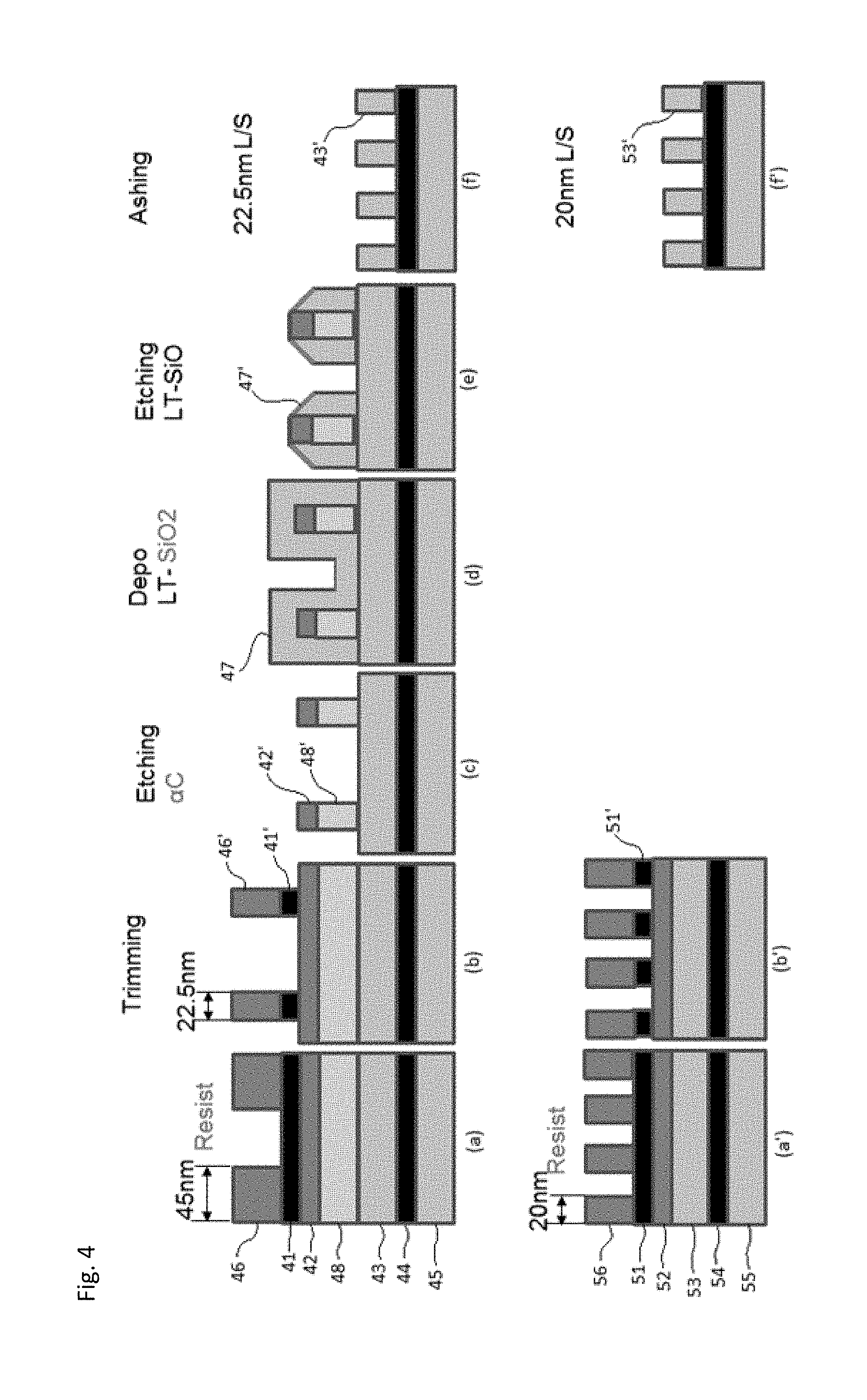
[0047] In advanced SDDP, step (b) is additionally conducted in order to lower the CD of a resist pattern, since it is difficult to form a resist pattern having a width of about 20 nm or smaller using ArF laser lithography. In step (a), a layered structure is constituted by an amorphous carbon layer (.alpha.C) 45 as a target layer (which is formed on a substrate (not shown), for example) prepared typically by a spin-on or CVD process, a silicon nitride layer (SiN) 44 deposited thereon to be used as an etch hard mask, an amorphous silicon layer (.alpha.Si) 43 deposited thereon to be used as a spacer, an amorphous carbon layer (.alpha.C) 48 as a template for double patterning, a silicon-containing anti-reflective coating (SiARC) 42 deposited thereon, a bottom anti-reflective coating (BARC) 41 (typically made of organic material) deposited thereon, and a photoresist pattern 46 (constituted by e.g., JSR3030, ARX 2014, or ARX 15327E manufactured by JSR Corporation, Tokyo, or a material equivalent thereto) formed typically by ArF laser lithography. The photoresist pattern 46 formed by ArF laser lithography has a width of 45 nm, for example.
[0048] In the advanced SDDP process, step (b) is performed to trim the resist 46 by dry etching (using e.g., O.sub.2, N.sub.2O, CO.sub.2, H.sub.2, or Ar, or a mixture of any two or more of the foregoing as an etchant gas, selected depending on the material constituting the resist) to reduce the CD of the resist pattern by reducing its width from 45 nm to 22.5 nm, thereby forming a trimmed resist 46'. The BARC 41 is also trimmed in the photoresist pattern to form a trimmed BARC 41' in step (b) which is a step of transferring a pattern to the .alpha.C 48 used as a template. In step (c), by using the trimmed resist 46' and the trimmed BARC 41', the SiARC 42 and the .alpha.C 48 are etched (using e.g., for silicon: HBr, Cl.sub.2, BCl.sub.3, Ar, O.sub.2, fluorine-containing gas (fluorocarbon, SF.sub.6, NF.sub.3); for carbon: O.sub.2, N.sub.2O, CO.sub.2, H.sub.2, Ar, H.sub.2, fluorine-containing gas (fluorocarbon, SF.sub.6, NF.sub.3) as an etchant gas) so as to transfer the pattern of the timed resist 46' to the SiARC 42 and the .alpha.C 48, forming an etched SiARC 42' and an etched .alpha.C 48'. In this embodiment, the BARC 41, SiARC 42, and .alpha.C 48 are used; however, these layers can be treated collectively as an anti-reflective layer used as a template which may be constituted by a single layer or multiple layers.
[0049] In step (d), a metal oxide layer (LT-SiO2) 47 (constituted by e.g., silicon oxide) is deposited at a relatively low temperature, followed by etching in step (e) which is a spacer RIE (reactive ion etch) step (using e.g., HBr, Cl.sub.2, BCl.sub.3, Ar, O.sub.2, fluorine-containing gas (fluorocarbon, SF.sub.6, NF.sub.3) as an etchant gas) to etch the metal oxide layer 47, forming an etched LT-SiO2 47'. By stripping the material of the etched SiARC 42' and the etched .alpha.C 48' by ashing, the etched LT-SiO2 47' is left on the .alpha.Si 43 as vertical spacers 84. Since the metal oxide spacer (47') has high etch selectivity, the etched SiARC 42' and the etched .alpha.C 48 (the template) for forming the spacer thereon can be thin and the metal oxide spacer (47') can be sustained during etching. In some embodiments, the thickness of the antireflective layers (constituted collectively by the BARC 41, the SiARC 42, and the .alpha.C 48) is about 5 to 50 nm (typically 10 to 30 nm), and the thickness of the metal oxide layer (LT-SiO2 47) is about 5 to 50 nm (typically 10 to 20 nm). In step (f), by using the etched LT-SiO2 47', the .alpha.Si 43 is etched (using e.g., HBr, Cl.sub.2, BCl.sub.3, Ar, O.sub.2, fluorine-containing gas (fluorocarbon, SF.sub.6, NF.sub.3) as an etchant gas), forming an etched .alpha.Si 43' which has a line width of 22.5 nm, for example, which can be used as a second template. As such, according to advanced SDDP, it is possible to form a template having a line width of about 22.5 nm, for example, even using ArF laser lithography.
[0050] However, as discussed above in relation to steps (a) to (f) in FIG. 4, advanced SDDP requires an intermediate template (e.g., the .alpha.C 48) and associated steps (c) to (e) involving additional etching and deposition steps. In contrast, in spacer-defined direct patterning as shown in steps (a'), (b'), and (f) in FIG. 4, additional steps (c) to (e) and also the intermediate template (e.g., the .alpha.C 48) can entirely be eliminated.
[0051] In direct patterning, in step (a'), by using EUV lithography, a resist pattern 56 having a line width of about 20 nm, for example, is formed on a layered structure constituted by layers 55, 54, 53, 52, and 51, which correspond or are equivalent to the amorphous carbon layer (.alpha.C) 45, the silicon nitride layer (SiN) 44, the amorphous silicon layer (.alpha.Si) 43, the silicon-containing anti-reflective coating (SiARC) 42, and the bottom anti-reflective coating (BARC) 41. In step (a'), the BARC 51 is trimmed in the resist pattern in step (a'), forming a trimmed BARC 51', and by using the trimmed BARC 51', the SiARC 52 and the .alpha.Si 53 are etched to transfer the resist pattern in step (b') to the .alpha.Si 53, forming an etched .alpha.Si 53' having a line width of 20 nm, for example, in step (f'). Accordingly, by using EUV lithography, a resist pattern having a line width of 10 nm to 20 nm can directly be transferred to a template without using an intermediate template.
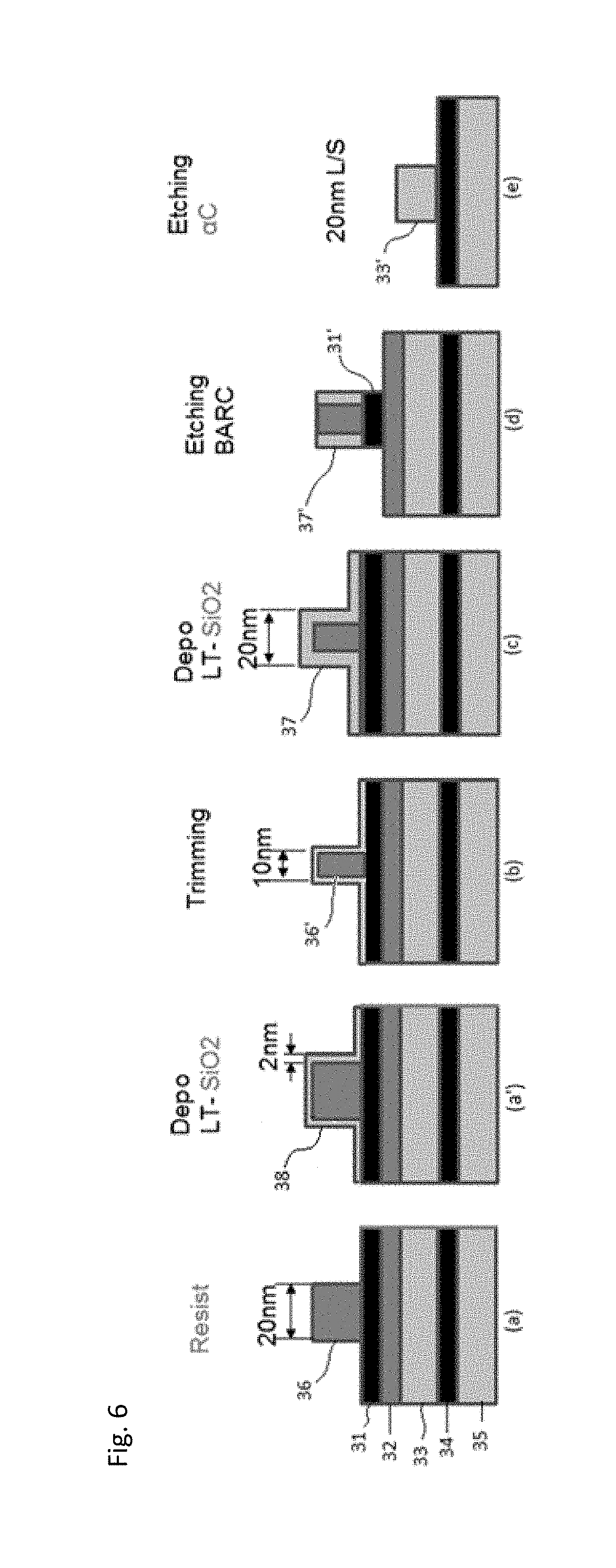
[0052] However, as mentioned earlier, although EUV lithography enables patterning with a pattern dimension of 10 to 20 nm, patterning accuracy, which is surface roughness evaluated by LER (Line-Edge Roughness) and LWR (Line-Width Roughness), depends on the characteristics of polymer constituting a resist, and thus, a surface roughness of approximately 5 nm may be the lower limit and has not yet improved.
[0053] FIG. 5 shows a schematic representation of pattern transfer (steps (a) to (e)) using spacer-defined direct patterning according to an embodiment of the present invention, in which the above described problem can effectively be resolved.
[0054] In direct patterning according to this embodiment, in step (a), by using EUV lithography, a resist pattern 36 having a line width of about 20 nm, for example (typically 10 nm to 20 nm), is formed on a layered structure constituted by layers 35, 34, 33, 32, and 31, which correspond or are equivalent to the amorphous carbon layer (.alpha.C) 55, the silicon nitride layer (SiN) 54, the amorphous silicon layer (.alpha.Si) 53, the silicon-containing anti-reflective coating (SiARC) 52, and the bottom anti-reflective coating (BARC) 51 in FIG. 4.
[0055] When using EUV lithography or equivalent thereto, a line width of a resist pattern can be as small as 20 nm or lower. However, LER (Line-Edge Roughness) and LWR (Line-Width Roughness) of the resist pattern are typically more than 3.5 nm and more than 5 nm, respectively, which are higher than desired LER and LWR for microfabrication of semiconductor devices, which are, for example, 3.5 nm or less (preferably 3 nm or less) and 5 nm or less (preferably 4 nm or less), respectively. In step (a) in FIG. 5, the LER and the LWR are, for example, 3.87 nm and 5.26 nm, respectively (see an Example described later).
[0056] According to this embodiment, in step (b) in FIG. 5, the resist 36 is trimmed so that the width of the resist 36 is reduced from 20 nm to 10 nm (typically 5 nm to 10 nm), forming a trimmed resist 36'. Through this dry etching process, the LER and the LWR can significantly be improved. For example, the LER and the LWR are reduced from 4.1 nm and 3.07 nm, respectively, to 5.26 nm and 3.87 nm, respectively, in step (b). In some embodiments, trimming can be performed under conditions shown in Table 1 below.
TABLE-US-00001 TABLE 1 (numbers are approximate) General Typical Temperature 30.degree. C. to 100.degree. C. 30.degree. to 50.degree. C. Pressure 100 Pa to 1000 Pa 200 Pa to 600 Pa Etchant O.sub.2, N.sub.2O, CO.sub.2, H.sub.2, Ar Selected depending on the resist material Etchant flow 1 to 10 SLM Selected depending on the resist material RF power for a 10 W to 500 W 30 W to 100 W 300-mm wafer Duration 1 to 20 seconds 5 to 10 seconds Trimming rate in 10 nm to 100 nm/min 20 nm to 50 nm/min width direction Trimming rate in 10 nm to 100 nm/min 20 nm to 50 nm/min height direction
[0057] In this disclosure, any indicated RF power for a 300-mm wafer can be converted to W/cm.sup.2 (wattage per unit area of a wafer) which can apply to a wafer having a different diameter such as 200 mm or 450 mm.
[0058] According to this embodiment, in step (c), a conformal metal oxide layer (LT-SiO2) 37 (constituted by, e.g., silicon oxide) is deposited by, e.g., PEALD at a relatively low temperature, on an exposed surface to compensate for the reduction of the width of the trimmed resist 36', so that the width of the line constituted by the trimmed resist 36' can be increased to or rebuilt to 20 nm, for example (typically 10 nm to 25 nm, which can be substantially the same as, thicker than, or thinner than the width of the resist in step (a)), by the deposited LT-SiO2 37 having a thickness of 5 nm (typically 2 nm to 10 nm). Since the LT-SiO2 37 is deposited by PEALD or the like and has a high conformality, it can cover the trimmed resist 36' uniformly at a uniform thickness, so that it can increase the width of the line without lowering its surface roughness. For example, the LER and the LWR of the line constituted by the oxide-covered trimmed resist are 2.63 nm and 3.64 nm, respectively. Since the LER and the LWR are expected to be maintained while transferring the line pattern to a template in step (e) in FIG. 5, the lines of the template can possess desirable LER and LWR.
[0059] In some embodiments, the oxide film in step (c) is constituted by SiO.sub.2, TiO, HfO, or AlO, which can be deposited under conventional conditions such as those disclosed in U.S. Pat. Nos. 8,252,691, and 8,298,951, each disclosure of which is incorporated herein by reference in its entirety. In some embodiments, the precursor for PEALD is an alkylaminosilane. In some embodiments, the alkylaminosilane is selected from the group consisting of bisdiethylaminosilane (BDEAS), bisdimethylaminosilane (BDMAS), hexylethylaminosilane (HEAD), tetraethylaminosilane (TEAS), tert-butylaminosilane (TBAS), bistert-butylaminosilane (BTBAS), bisdimethylaminodimethylaminosilane (BDMADMS), heptametyldisilazane (HIVIDS), trimethysylyldiethlamine (TMSDEA), trimethylsyledimethlamine (TMSDMA), trimethyltoribinylcycletrisilazane (TMTVCTS), tri strimetylhydroxyamine (TTMSHA), bisdimethylsaminomethylsilane (BDMAMS), and dimetyhlsilyldimethlamine (DMSDMA). The precursor can be constituted by a single precursor or a mixture of two or more precursors. In some embodiments, the oxide film has a conformality of 80% to 100% (typically about 90% or higher) wherein the "conformality" is determined by comparing film thickness deposited at some point (typically a midway point) on a sidewall or on a bottom of a recess to film thickness deposited on a flat surface just outside the recess.
[0060] In step (d) in FIG. 5, the BARC 31 is trimmed in the resist pattern in step (c), forming a trimmed BARC 31', and by using the trimmed BARC 31', the SiARC 32 and the .alpha.Si 33 are etched to transfer the resist pattern in step (c) to the .alpha.Si 33, forming an etched .alpha.Si 33' having a line width of 20 nm, for example, in step (e). According to this embodiment, by using EUV lithography, a resist pattern having a line width of 10 nm to 20 nm can directly be transferred to a template while improving the LER and LWR. In some embodiments, etching in step (d) following step (c) can be performed under conditions shown in Table 2 below.
TABLE-US-00002 TABLE 2 (numbers are approximate) General Typical Temperature 20.degree. C. to 100.degree. C. 40.degree. C. to 60.degree. C. Pressure 3 Pa to 10 Pa 4 Pa to 8 Pa Etchant O.sub.2, N.sub.2O, CO.sub.2, H.sub.2, Ar Selected depending on the materials of oxide and anti-reflective layer Etchant flow 0.01 to 0.3 SLM Selected depending on the materials of oxide and anti-reflective layer RF power for a 100 W to 1000 W 300 W to 500 W 300-mm wafer Duration 5 to 120 seconds 10 to 30 seconds Trimming rate in 0.3 nm to 10 nm/min 0.5 nm to 2 nm/min width direction Trimming rate in 30 nm to 300 nm/min 50 nm to 100 nm/min height direction
[0061] In step (c) in FIG. 5, in some embodiments, the film profile and film quality of the metal oxide layer 37 can be manipulated in order to achieve a desired result in steps (d) and (e), i.e., when transferring the resist pattern to the template. For example, by depositing the metal oxide film 37 in a manner where a film deposited on a top surface of the trimmed resist 36' has selectively a thickness greater than that of a film deposited on side surfaces of the trimmed resist 36' and/or a chemical resistance (represented by dry etch rate and/or wet etch rate) higher than that of the film deposited on the side surfaces of the trimmed resist 36' so that the height of the oxide-covered trimmed resist can be maintained while dry or wet etching of the BARC 31 progresses in step (d). For example, the wet etch rate of the film deposited on the side surfaces is at least two times (e.g., 2 to 5 times) the wet etch rate of the film deposited on the top surface. Such selective tuning of thickness and quality of the film can be achieved according to the technology disclosed in, e.g., U.S. Ser. No. 15/048,422, filed Feb. 19, 2016, U.S. Ser. No. 15/592,730, filed May 11, 2017, and U.S. Ser. No. 15/650,686, filed Jul. 14, 2017, by the same applicant as in the instant application, each disclosure of which is incorporated herein by reference in its entirety.
[0062] In step (b) in FIG. 5, the trimming process can be conducted by conventional methods. However, because the trimming speed of the resist is controlled mainly by the radical density surrounding the resist, the trimming speed varies depending on the density of the resist pattern, i.e., whether the pattern is sparse or dense defined by, e.g., a distances or intervals between lines. A variation of trimming speed depending on the density of a pattern is called the "loading effect." Thus, due to the loading effect, when the resist pattern is constituted by lines arranged at different pitches or intervals, the trimming speed of lines densely arranged is lower than that of lines sparsely arranged (fewer radicals enter into narrow valleys (trenches) than into wide valleys (trenches)), resulting in variations of line width or CD.
[0063] In this disclosure, a recess between adjacent photoresist lines, vertical spacers, and any other recess pattern is referred to as a "line space". In some embodiments, the pattern is constituted by lines having different line spaces varying from about 10 nm to about 100 nm (typically about 20 nm to about 50 nm). In that case, the "loading effect" emerges, resulting in varying the line width and lowering LER/LWR.
[0064] FIG. 6 shows a schematic representation of pattern transfer (steps (a) to (e) with additional step (a')) using spacer-defined direct patterning according to another embodiment of the present invention, in which steps (a) to (e) are equivalent to those shown in FIG. 5, except for step (a'). Considering the above-discussed problem in the conventional trimming method, in this embodiment, step (a') is additionally conducted, in which a conformal thin metal oxide layer (LT-SiO2, constituted by, e.g., silicon oxide) 38 is deposited by PEALD at a relatively low temperature at a small thickness (typically 0.5 nm to 5 nm, e.g., 2 nm or less, more typically 1 nm to 2 nm). By depositing the thin oxide layer 38 contacting and covering the exposed surface of the resist 36, when the oxide-covered resist is exposed to oxygen radicals in step (b), the trimming speed of the resist is not predominantly or directly controlled by the radical density since the thin oxide layer covers the resist surface, but is rather controlled by the diffusion speed of oxygen radicals through the thin oxide layer and/or the quantity of reactive oxygen (free radicals) generated by ion bombardment to the thin oxide layer, thereby alleviating the loading effect and improving uniformity of line width and line space throughout the pattern. The thickness of the thin oxide layer can be determined based on the compatibility or affinity between the resist and the oxide layer, etc.; however, when the thickness of the oxide layer is more than 5 nm, radicals cannot reach the resist surface through the oxide layer, and thus, trimming cannot effectively be performed. When the thin oxide layer is exposed to oxygen radicals, the thin oxide layer functions as a buffer layer, and oxygen radicals are regenerated through the thin oxide layer, trimming the resist, in which when trimming progresses, the width of the resist gradually decreases while keeping the thin oxide layer attached to the resist wherein the thickness of the thin oxide layer also gradually decreases. In some embodiments, trimming in step (b) following step (a') can be performed under conditions shown in Table 3 below.
TABLE-US-00003 TABLE 3 (numbers are approximate) General Typical Temperature 30.degree. C. to 100.degree. C. 30.degree. C. to 75.degree. C. Pressure 100 Pa to 1000 Pa 200 Pa to 600 Pa Etchant O.sub.2, N.sub.2O, CO.sub.2, H.sub.2, Ar Selected depending on the materials of oxide and resist Etchant flow 0.01 to 2 SLM Selected depending on the materials of oxide and resist RF power for a 10 W to 500 W 30 W to 100 W 300-mm wafer Duration 5 to 300 seconds 10 to 30 seconds Trimming rate in 1 nm to 50 nm/min 5 nm to 15 nm/min width direction Trimming rate in 0 nm to 10 nm/min 0 nm to 5 nm/min height direction
[0065] It should be noted that when depositing the thin oxide layer by PEALD on the resist, since PEALD generates more radicals and creates more ion bombardment than does thermal ALD or radical ALD (remote plasma), the resist surface is trimmed to a certain extent in step (a'), although such a phenomenon is not illustrated in step (a') in FIG. 6 (Plasma CVD may not be suitable for depositing the oxide layer because it is not suitable for depositing a conformal layer). Thus, the width of the resist is reduced not only in step (b) but also in step (a'). The above-described phenomenon (trimming takes place while depositing) can be seen or confirmed by observing a STEM photograph of a cross section of the resist or by measuring an increase of the line width in step (a') which is lower than that in the case where the same layer is deposited under the same conditions except that the layer is deposited on a chemically stable non-resist material. When step (a') serves as the above-discussed trimming/depositing step, the trimmed quantity of the resist can be controlled using the substrate temperature and the plasma power as process parameters wherein the trimmed quantity becomes higher when the substrate temperature is higher (the reactivity of oxygen is higher) and the plasma power is higher (also the reactivity of oxygen is higher).
[0066] In some embodiments, the oxide layer deposited in step (a') is identical to or different from the oxide layer deposited in step (c). In some embodiments, steps (a) through (c) in FIG. 6 are continuously conducted in the same reaction chamber of a PEALD apparatus, and then steps (d) and (e) are continuously conducted in an etching apparatus. In the above, "continuously" refers to without moving the substrate from the same chamber, without a materially different intervening step, or without an intervening step of a materially different recipe. In some embodiments, the trimming in step (b) is typically conducted by using direct plasma (in situ plasma etching), and alternatively, it can be conducted using remote plasma or the like as long as the resist can be exposed directly to a plasma. However, direct plasma is preferable when the trimming in step (b) is conducted after step (a') in FIG. 6, as compared with the trimming in step (b) without step (a') in FIG. 5, because direct plasma contains not only radicals but also a significant quantity of ions, as compared with remote plasma (steps (a') followed by step (b) requires both radicals and ions). In some embodiments, the trimming in step (b) is conducted using an Ar/N.sub.2 plasma, rather than an O.sub.2 plasma, because an Ar/N.sub.2 plasma etching involves slow etching speed and thus, it is easier to control or manipulate the trimmed quantity. On the other hand, the deposition of the oxide layer in step (a') (and in some embodiments, also in step (c)) is conducted using an oxygen plasma.
[0067] The process sequence from step (b) to step (d) in FIG. 5 and that from step (a') to step (d) in FIG. 6 can be conducted continuously in the same reaction chamber, wherein each step is controlled by a particular recipe, and a purging/gas stabilization step may be conducted between different recipes, without transferring a substrate from the reaction chamber or without exposing the substrate to outside air. These processes can be performed using any suitable apparatus including an apparatus illustrated in FIG. 1, for example. FIG. 1 is a schematic view of a PEALD apparatus, desirably in conjunction with controls programmed to conduct the sequences described below, usable in some embodiments of the present invention. In this figure, by providing a pair of electrically conductive flat-plate electrodes 4, 2 in parallel and facing each other in the interior 11 (reaction zone) of a reaction chamber 3, applying HRF power (13.56 MHz or 27 MHz) 25 to one side, and electrically grounding the other side 12, a plasma is excited between the electrodes. A temperature regulator is provided in a lower stage 2 (the lower electrode), and a temperature of a substrate 1 placed thereon is kept constant at a given temperature. The upper electrode 4 serves as a shower plate as well, and reactant gas and/or dilution gas, if any, and precursor gas and etchant gas are introduced separately into the reaction chamber 3 through a gas line 21 and a gas line 22 (other gas line(s) are omitted), and through the shower plate 4, according to a given recipe set for each step. Additionally, in the reaction chamber 3, a circular duct 13 with an exhaust line 7 is provided, through which gas in the interior 11 of the reaction chamber 3 is exhausted. Additionally, a transfer chamber 5 disposed below the reaction chamber 3 is provided with a seal gas line 24 to introduce seal gas into the interior 11 of the reaction chamber 3 via the interior 16 (transfer zone) of the transfer chamber 5 wherein a separation plate 14 for separating the reaction zone and the transfer zone is provided (a gate valve through which a wafer is transferred into or from the transfer chamber 5 is omitted from this figure). The transfer chamber is also provided with an exhaust line 6.
[0068] In some embodiments, step (e) (etching step) can be conducted in any etching apparatus including a conventional apparatus. Depending on the material constituting a layer to be removed, i.e., depending on its resistance or sensitivity to e.g., HF, HCl, and TMAH wet etch; e.g. to BCl.sub.3, BCl.sub.3/Ar, dry etch; or e.g., to oxidation, a combination of wetetch chemistry alternating oxidizing and HF (common in semiconductor processing), or dry etch based on oxygen or CF.sub.4, for example, the etching conditions are selected, and etching is conducted accordingly.
[0069] A skilled artisan will appreciate that the apparatus includes one or more controller(s) (not shown) programmed or otherwise configured to cause the deposition and reactor cleaning processes described elsewhere herein to be conducted. The controller(s) are communicated with the various power sources, heating systems, pumps, robotics and gas flow controllers or valves of the reactor, as will be appreciated by the skilled artisan.
[0070] In some embodiments, a dual chamber reactor (two sections or compartments for processing wafers disposed closely to each other) can be used, wherein a reactant gas and a noble gas can be supplied through a shared line whereas a precursor gas is supplied through unshared lines.
[0071] The present invention is further explained with reference to working examples below. However, the examples are not intended to limit the present invention. In the examples where conditions and/or structures are not specified, the skilled artisan in the art can readily provide such conditions and/or structures, in view of the present disclosure, as a matter of routine experimentation. Also, the numbers applied in the specific examples can be modified by a range of at least .+-.50% in some embodiments, and the numbers are approximate.
EXAMPLES
Example 1
[0072] A photoresist pattern (constituted by e.g., Novolacs designed for EUV lithography) formed on a SiOC layer of a 300-mm substrate and having an initial CD of about 35 nm was subjected to trimming using a PEALD apparatus illustrated in FIG. 1A under conditions shown in Table 4 below.
TABLE-US-00004 TABLE 4 (numbers are approximate) Conditions for trimming Resist material EUV resist Temperature 75.degree. C. Pressure 200 Pa Etchant O.sub.2 Etchant flow 1 SLM RF power for a 300-mm wafer 30 W Duration Varied (see FIG. 2) Trimming rate in width direction 1.4 nm/sec Trimming rate in height direction 2 nm/sec
[0073] FIG. 3 is a graph showing the relationship between CD of the photoresist ("PR CD") and process times of trimming ("Process time"). It is confirmed that CD of the photoresist was reduced linearly as a function of process time of trimming at least to the degree that CD was as low as about 20 nm.
Example 2
[0074] Even though EUV lithography has higher exposure accuracy than ArF laser, it is difficult to reduce the CD (Critical Dimension) of a resist pattern to the degree which is as low as 12 nm or lower. In this example, a photoresist was subjected to trimming in a manner substantially similar to that in Example 1 except that the initial CD of the photoresist was about 17.9 nm. FIG. 2 shows SEM photographs of patterned surfaces after EUV lithography without trimming ("After litho"), after 0.5 seconds of trimming ("0.5 s"), after 1.0 seconds of trimming ("1 s"), after 1.5 seconds of trimming ("1.5 s"), and after 2.0 seconds of trimming ("2 s"), wherein the lower photos (b) are taken at a higher magnification than that for the upper photos (a).
[0075] As can be seen in FIG. 2, as trimming of the resist pattern progressed, the CD of the resist pattern was reduced from about 17.9 nm (without trimming), about 16 nm (0.5 sec. of trimming), about 15.1 nm (1 sec. of trimming), about 14.5 nm (1.5 sec. of trimming), and about 12.3 nm (2 sec. of trimming). However, as can also be seen in FIG. 2, the contrast between line areas and non-line areas became low as the trimming progressed, i.e., starting the occurrence of line interruption. It is confirmed that it was difficult to reduce the CD of the resist pattern to about 12 nm or lower.
Example 3
[0076] In this example, a photoresist (ArF resist with an initial CD of about 7.90 nm (mean)) was subjected to trimming in a manner similar to that in Example 1 under the conditions shown in Table 5 below.
TABLE-US-00005 TABLE 5 (numbers are approximate) Conditions for trimming Resist material ArF resist Temperature 75.degree. C. Pressure 200 Pa Etchant O.sub.2 Etchant flow 2 SLM RF power for a 300-mm wafer 30 W Duration 13.2 seconds Trimming rate in width direction 0.93 nm/sec Trimming rate in height direction Not measured
[0077] The trimmed resist pattern was then subjected to SiO.sub.2 deposition by PEALD which was conducted under the conditions shown in Table 6 below.
TABLE-US-00006 TABLE 6 (numbers are approximate) Conditions for PEALD Substrate temperature 75.degree. C. Electrode gap (a thickness of a substrate is 10 mm about 0.7 mm) Pressure 500 Pa Precursor BDEAS Carrier gas/Dilution gas Ar Flow rate of carrier gas (continuous) 1000 sccm Flow rate of dilution gas (continuous) 1000 sccm Flow rate of precursor Corresponding to the flow rate of carrier gas RF power (13.56 MHz) for a 300-mm wafer 50 W Duration of "Feed" 0.2 sec. Duration of "Purge 1" 0.2 sec. Duration of "RF" 0.2 sec. Duration of "Purge 2" 0.2 sec. Duration of one cycle 0.8 sec. GPC ({acute over (.ANG.)}/cycle) 1 Thickness of the film 17.6 nm
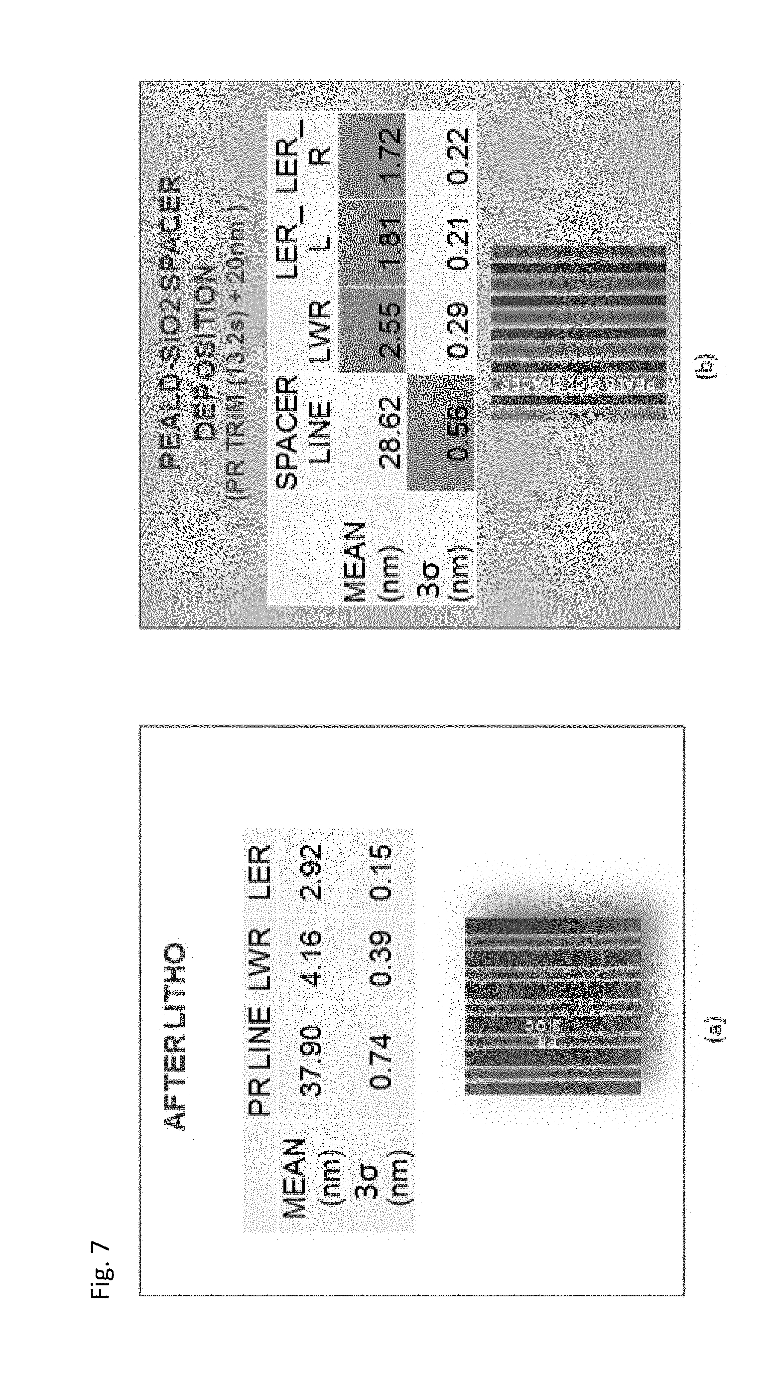
[0078] FIG. 7 shows STEM photographs of patterned lines of a photoresist formed by photolithography ("AFTER LITHO" in (a)) and after deposition of a silicon oxide film ("PEALD-SIO2 SPACER DEPOSITION" in (b)) wherein "3.sigma." stands for 3 standard deviation of the mean). In this example, although the initial CD of the resist pattern was about 38 nm (mean) as shown in (a) of FIG. 7, whereas the CD of the oxide-covered trimmed resist was about 29 nm (mean) as shown in (b) of FIG. 7, the width of the oxide-covered trimmed resist pattern is considered to be substantially the same as that of the initial resist (since the width of the trimmed resist pattern was about 9 nm and that of the oxide-covered trimmed resist pattern was about 29 nm, which was considered to be substantial size recovery with reference to a width of 38 nm). As shown in FIG. 7, the oxide-covered trimmed resist pattern manifested significant improvement on LWR and LER, as compared with the initial resist pattern.
Example 4
[0079] In this example, a photoresist was subjected to trimming, followed by oxide deposition, in a manner substantially similar to that in Example 3 except that the initial CD of the photoresist was about 44.5 nm, the trimming was conducted for 9 seconds, and the CD of the oxide-covered trimmed resist was recovered to about 62.8 nm. Although the initial CD of the resist pattern was about 45 nm, whereas the CD of the oxide-covered trimmed resist was about 63 nm, the width of the oxide-covered trimmed resist pattern is considered to be substantially the same as that of the initial resist (since the width of the trimmed resist pattern was about 28 nm and that of the oxide-covered trimmed resist pattern was about 63 nm, which was considered to be substantial size recovery with reference to a width of about 45 nm).
[0080] FIG. 8 shows STEM photographs of patterned lines of a photoresist formed by photolithography ("After litho"), after 9 seconds of trimming ("After 9 s trim"), and after deposition of an oxide film ("After spacer dep"). FIG. 8 also shows CD, LWR, and LER thereof. As shown in FIG. 8, the oxide-covered trimmed resist pattern manifested significant improvement on LWR and LER, as compared with the initial resist pattern.
Example 5
[0081] In this example, a photoresist was subjected to trimming in a manner substantially similar to that in Example 4 except that the trim time was varied as shown in FIG. 9. FIG. 9 is a graph showing the relationship between LER and LWR of a photoresist ("LER/LWR") and process times of trimming ("Trim time") wherein "POR" refers to "point of reference". As shown in FIG. 9, the trimmed resist pattern manifested significant improvement on LWR and LER until reaching a plateau when increasing the trim time. FIG. 10 is a table showing CD corresponding to the measuring points shown in FIG. 9. As shown in FIG. 10, CD also was decreased by increasing the process time of trimming.
[0082] Example 6
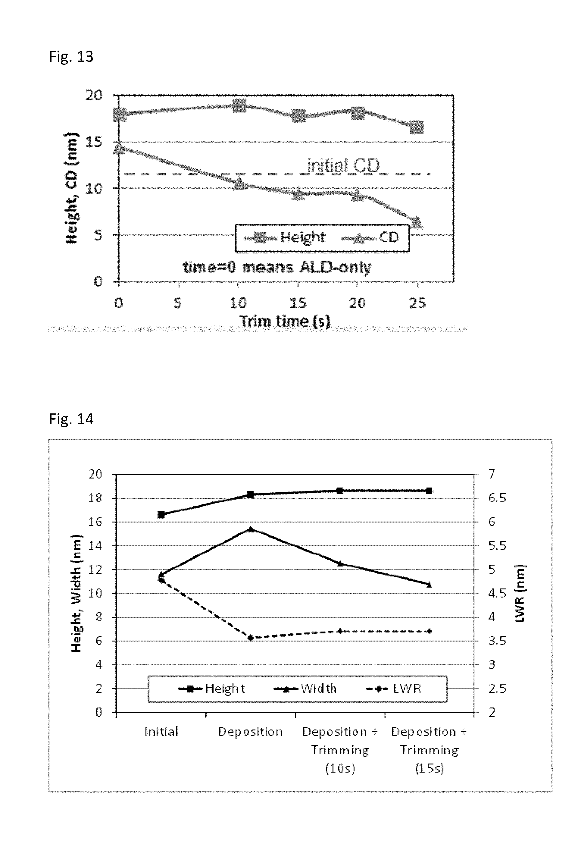
[0083] In this example, a photoresist (EUV resist with an initial CD of about 11 nm) was subjected to SiO deposition by PEALD in a manner substantially similar to that in Example 3 except that the film thickness was about 2 nm, followed by trimming in a manner substantially similar to that in Example 1 except that the trim time was varied as shown in FIG. 12. FIG. 11 shows STEM photographs of cross-sectional views of patterned lines of a photoresist formed by photolithography ("initial" in (a)) and after depositing a SiO layer by ALD thereon ("SiO ALD (.about.2 nm)" in (b)). FIG. 12 shows STEM photographs of cross-sectional views of patterned lines after depositing the SiO layer by ALD shown in (b) of FIG. 11 ("SiO ALD (.about.2 nm)" in (b)), after trimming the patterned lines for 10 seconds ("ALD+trim(10 s)" in (c)), after trimming the patterned lines for 15 seconds ("ALD+trim(15 s)" in (d)), and after trimming the patterned lines for 20 seconds ("ALD+trim(20 s)" in (e)). FIG. 13 is a graph showing changes in height and CD (nm) of the patterned lines when the trimming time changed as shown in FIG. 12.
[0084] As shown in FIG. 11, a conformal SiO thin film (having a thickness of about 2 nm) was deposited evenly over the resist pattern including sidewalls and bottom areas thereof. As shown in FIG. 12, it was confirmed that trimming could be performed without substantially lowering the height of the spacers (the patterned resist). This appeared to be because the SiO thin film could serve as a source of active species such as oxygen radicals generated and supplied to underlying surfaces of the resist for etching when being exposed to a plasma. That is, the SiO thin film could significantly protect the resist by mitigating strikes by ion bombardment of a plasma, thereby suppressing predominant etching at the top and bottom areas of the resist, and could release active species rather evenly to the resist surfaces for etching, thereby etching the sidewall areas more than the top and bottom areas of the resist since the sidewall areas are much less chemical-resistant than the top and bottom areas (e.g., the sidewall layer is less densified and has a twice or higher WER than the top and bottom layers, which can also represent DER). For the same reason, the loading effect could be ameliorated (i.e., uniform etching could be conducted regardless of whether the resist pattern had narrow intervals or wide intervals), thereby decreasing CD of the resist pattern without lowering the height of the pattern. However, as shown in FIG. 13, when the trim time exceeded 20 seconds, the height of the pattern tended to start decreasing.
Example 7
[0085] In this example, a photoresist (EUV resist with an initial CD of about 11 nm) was subjected to SiO deposition by PEALD, followed by trimming, in a manner substantially similar to that in Example 6. FIG. 14 is a graph showing changes in height, width (nm), and LWR (nm) of patterned lines when the trimming time changed. FIG. 15 shows STEM photographs of cross-sectional views of patterned lines before depositing the SiO layer by ALD in (a) corresponding to the "initial" in FIG. 14, after depositing the SiO layer by ALD in (b) corresponding to the "Deposition" in FIG. 14, after trimming the patterned lines for 10 seconds in (c) corresponding to the "Deposition+Trimming (10 s)" in FIG. 14, and after trimming the patterned lines for 15 seconds in (d) corresponding to the "Deposition+Trimming (15 s)" in FIG. 14. As shown in FIG. 14, the results were similar to those shown in Example 6. In addition, as shown in FIG. 14, LWR was improved by depositing the SiO thin film and remained improved while trimming the spacers (the patterned resist).
Prophetic Example 1
[0086] According to the sequence shown in FIG. 6, first, a substrate with a resist pattern (EUV resist) 36 is prepared, which has a layer structure shown in (a) of FIG. 6. Next, the resist pattern is subjected to deposition of SiO thin film 38 at a low temperature in a manner substantially similar to that shown in Example 3 (the deposition time or the like may be adjusted), as shown in (a') of FIG. 6. The oxide-covered resist pattern is then subjected to trimming in a manner substantially similar to that shown in Example 1 (the trim time or the like may be adjusted), obtaining the resist pattern 36' having a narrow width without lowering the height, as shown in (b) of FIG. 6. Thereafter, the trimmed resist pattern is subjected to SiO deposition in a manner substantially similar to that shown in Example 3 (the deposition time or the like may be adjusted) so as to cover the trimmed resist with SiO film 37 (referred to as "spacers") to render the width of the spacers 37 substantially the same as that of the initial resist 36, as shown in (c) of FIG. 6. Next, the spacers 36 are subjected to template etching (anisotropic etching) to etch the BARC layer 31 using the spacers as an etching mask, under conditions shown in Table 7 below, as shown in (d) of FIG. 6. Next, using the etching mask constituted by the spacers 37' and the etched BARC 31', the template is further subjected to anisotropic etching under conditions shown in Table 8 below so as to transfer the etching mask pattern to the .alpha.Si layer 33 to obtain a patterned .alpha.Si layer 33', as shown in (e) of FIG. 6.
TABLE-US-00007 TABLE 7 (numbers are approximate) Temperature 60.degree. C. Pressure 5 Pa Etchant Ar/O.sub.2/CF.sub.4 Etchant flow 200/50/20 sccm RF power for a 300-mm wafer 200 W Duration 20 seconds Trimming rate in width direction Substantially zero
TABLE-US-00008 TABLE 8 (numbers are approximate) Temperature 60.degree. C. Pressure 1 Pa Etchant Ar/O.sub.2 Etchant flow 200/200 sccm RF power for a 300-mm wafer 500 W Duration 60 seconds Trimming rate in width direction Substantially zero
[0087] As a result, the patterned .alpha.Si 33' having substantially the same CD as that of the initial resist pattern 36 with significantly improved (reduced) LWR and LER can be obtained, confirming that direct patterning as shown in (a'), (b'), and (f) of FIG. 4 is successfully performed.
Prophetic Example 2
[0088] According to the sequence shown in FIG. 5, a resist pattern (EUV resist) 36 is transferred to an .alpha.Si layer 33 of a template in a manner substantially similar to that in Prophetic Example 1 except that step (a') of Prophetic Example 1 was omitted.
[0089] As a result, the patterned .alpha.Si 33' having substantially the same CD as that of the initial resist pattern 36 with significantly improved (reduced) LWR and LER can be obtained, confirming that direct patterning as shown in (a'), (b'), and (f) of FIG. 4 is successfully performed.
[0090] It will be understood by those of skill in the art that numerous and various modifications can be made without departing from the spirit of the present invention. Therefore, it should be clearly understood that the forms of the present invention are illustrative only and are not intended to limit the scope of the present invention.
* * * * *
D00000
D00001
D00002
D00003
D00004
D00005
D00006
D00007
D00008
D00009
D00010
D00011
D00012
XML
uspto.report is an independent third-party trademark research tool that is not affiliated, endorsed, or sponsored by the United States Patent and Trademark Office (USPTO) or any other governmental organization. The information provided by uspto.report is based on publicly available data at the time of writing and is intended for informational purposes only.
While we strive to provide accurate and up-to-date information, we do not guarantee the accuracy, completeness, reliability, or suitability of the information displayed on this site. The use of this site is at your own risk. Any reliance you place on such information is therefore strictly at your own risk.
All official trademark data, including owner information, should be verified by visiting the official USPTO website at www.uspto.gov. This site is not intended to replace professional legal advice and should not be used as a substitute for consulting with a legal professional who is knowledgeable about trademark law.