Method Of Forming A Transition Metal Containing Film On A Substrate By A Cyclical Deposition Process, A Method For Supplying A T
Hatanpaa; Timo ; et al.
U.S. patent application number 15/897578 was filed with the patent office on 2019-08-15 for method of forming a transition metal containing film on a substrate by a cyclical deposition process, a method for supplying a t. The applicant listed for this patent is ASM IP Holding B.V.. Invention is credited to Timo Hatanpaa, Markku Leskela, Mikko Ritala, Katja Vayrynen.
| Application Number | 20190249300 15/897578 |
| Document ID | / |
| Family ID | 66397263 |
| Filed Date | 2019-08-15 |


| United States Patent Application | 20190249300 |
| Kind Code | A1 |
| Hatanpaa; Timo ; et al. | August 15, 2019 |
METHOD OF FORMING A TRANSITION METAL CONTAINING FILM ON A SUBSTRATE BY A CYCLICAL DEPOSITION PROCESS, A METHOD FOR SUPPLYING A TRANSITION METAL HALIDE COMPOUND TO A REACTION CHAMBER, AND RELATED VAPOR DEPOSITION APPARATUS
Abstract
A method of forming a transition metal containing films on a substrate by a cyclical deposition process is disclosed. The method may include: contacting the substrate with a first vapor phase reactant comprising a transition metal halide compound comprising a bidentate nitrogen containing adduct ligand; and contacting the substrate with a second vapor phase reactant. A method for supplying a transition metal halide compound comprising a bidentate nitrogen containing ligand to a reaction chamber is disclosed, along with related vapor deposition apparatus.
| Inventors: | Hatanpaa; Timo; (Espoo, FI) ; Vayrynen; Katja; (Helsinki, FI) ; Ritala; Mikko; (Espoo, FI) ; Leskela; Markku; (Espoo, FI) | ||||||||||
| Applicant: |
|
||||||||||
|---|---|---|---|---|---|---|---|---|---|---|---|
| Family ID: | 66397263 | ||||||||||
| Appl. No.: | 15/897578 | ||||||||||
| Filed: | February 15, 2018 |
| Current U.S. Class: | 1/1 |
| Current CPC Class: | C23C 16/45553 20130101; H01L 21/768 20130101; C23C 16/45523 20130101; H01L 21/28568 20130101; C23C 16/45527 20130101; H01L 23/53209 20130101; H01L 23/53238 20130101; H01L 21/76843 20130101; C23C 16/406 20130101; H01L 21/76879 20130101 |
| International Class: | C23C 16/455 20060101 C23C016/455; H01L 21/285 20060101 H01L021/285; H01L 23/532 20060101 H01L023/532; C23C 16/40 20060101 C23C016/40 |
Claims
1. A method of forming a transition metal containing film on a substrate by a cyclical deposition process, the method comprising: contacting the substrate with a first vapor phase reactant comprising a transition metal halide compound comprising a bidentate nitrogen containing adduct ligand; and contacting the substrate with a second vapor phase reactant.
2. The method of claim 1, wherein the adduct ligand comprises two nitrogen atoms, each of nitrogen atoms bonded to at least one carbon atom.
3. The method of claim 1, wherein the transition metal halide compound comprise a transition metal chloride.
4. The method of claim 3, wherein the transition metal chloride compound comprises at least one of a cobalt chloride, a nickel chloride, or a copper chloride.
5. The method of claim 4, wherein the transition metal chloride compound comprises at least one of cobalt chloride (TMEDA), or nickel chloride (TMPDA).
6. The method of claim 1, wherein the second vapor phase reactant comprises an oxygen precursor selected from the group consisting of ozone (O.sub.3), molecular oxygen (O.sub.2), oxygen atoms (O), an oxygen plasma, oxygen radicals, oxygen excited species, water (H.sub.2O), and hydrogen peroxide (H.sub.2O.sub.2).
7. The method of claim 6, wherein the transition metal containing film comprises a transition metal oxide.
8. The method of claim 7, wherein the transition metal oxide substantially comprises cobalt (II) oxide (CoO).
9. The method of claim 7, further comprising contacting the transition metal oxide with a reducing agent precursor thereby forming an elemental transition metal.
10. The method of claim 9, wherein the reducing agent precursor comprises at least one of forming gas (H.sub.2+N.sub.2), ammonia (NH.sub.3), hydrazine (N.sub.2H.sub.4), molecular hydrogen (H.sub.2), hydrogen atoms (H), a hydrogen plasma, hydrogen radicals, hydrogen excited species, alcohols, aldehydes, carboxylic acids, boranes, or amines.
11. The method of claim 1, further comprising contacting the substrate with a third vapor phase reactant comprising a reducing agent precursor selected from the group consisting of tertiary butyl hydrazine (C.sub.4H.sub.12N.sub.2), hydrogen (H.sub.2), a hydrogen (H.sub.2) plasma, ammonia (NH.sub.3), an ammonia (NH.sub.3) plasma, hydrazine (N.sub.2H.sub.4), silane (SiH.sub.4), disilane (Si.sub.2H.sub.6), trisilane (Si.sub.3H.sub.8), germane (GeH.sub.4), digermane (Ge.sub.2H.sub.6), borane (BH.sub.3), and diborane (B.sub.2H.sub.6).
12. The method of claim 1, wherein the transition metal containing film comprises at least one of elemental cobalt, elemental nickel, or elemental copper.
13. The method of claim 1, wherein the cyclical deposition process comprises an atomic layer deposition process.
14. The method of claim 1, wherein the cyclical deposition process comprises a cyclical chemical vapor deposition process.
15. The method of claim 1, wherein the transition metal containing film comprises at least one of an elemental transition metal, a transition metal nitride, a transition metal silicide, a transition metal sulfide, a transition metal selenide, a transition metal phosphide, or a transition metal boride.
16. A method of forming a transition metal containing film on a substrate by a cyclical deposition process, the method comprising: contacting the substrate with a first vapor phase reactant comprising a transition metal compound comprising an adduct forming ligand; and contacting the substrate with a second vapor phase reactant; wherein the transition metal is selected group consisting of copper (Cu), nickel (Ni), and cobalt (Co).
17. The method of claim 16, wherein the adduct forming ligand comprises at least one of nitrogen, phosphorous, oxygen, or sulfur.
18. The method of claim 16, wherein the transition metal compound comprises a transition metal halide compound, selected from the group consisting of a transition metal chloride, a transition metal iodide, a transition metal fluoride, or a transition metal bromide.
19. The method of claim 18, wherein the transition metal halide compound comprises a bidentate nitrogen adduct forming ligand.
20. The method of claim 16, wherein the transition metal compound comprises at least one of cobalt chloride (TMEDA), cobalt bromide (TMEDA), cobalt iodide (TMEDA), cobalt chloride (TMPDA), or nickel chloride (TMPDA).
21. The method of claim 16, wherein the transition metal compound comprising an adduct forming ligand is synthesized utilizing a one-step synthesis process comprising, combining a transition metal halide compound and an adduct forming ligand at a temperature of less than 50.degree. C.
22. The method of claim 16, wherein the second vapor phase reactant comprises at least one of a oxygen precursor, a nitrogen precursor, a silicon precursor, a sulfur precursor, a selenium precursor, a phosphorous precursor, a boron precursor, or a reducing agent.
23. A device structure including the transition metal containing film formed according to the method of claim 1.
24. A method for supplying a transition metal halide compound comprising a bidentate nitrogen containing adduct ligand to a reaction chamber, the method comprising: providing a precursor source vessel configured for containing the transition metal halide compound; fluidly connecting the precursor source vessel to the reaction chamber; heating the transition metal halide compound contained in the precursor source vessel to a temperature greater than 50.degree. C.; generating a vapor pressure of the transition metal halide compound of least at least 0.001 mbar; and supplying the transition metal halide compound to the reaction chamber.
25. The method of claim 24, wherein the transition metal halide compound comprises at least one of cobalt chloride (TMEDA), nickel chloride (TMPDA).
26. A vapor deposition apparatus utilizing reactive volatile chemicals, the apparatus comprising: a reaction chamber; a substrate disposed in the reaction chamber; a precursor source vessel in fluid communication with the reaction chamber; and a transition metal halide compound comprising a bidentate nitrogen containing adduct ligand disposed in the precursor source vessel.
27. The apparatus of claim 26, wherein the transition metal halide compound comprises at least one of cobalt chloride (TMEDA), or nickel chloride (TMPDA).
28. The apparatus of claim 26, wherein the transition metal compound exhibits a vapor pressure of greater than 0.001 mbar at a transition metal compound temperature of less than 150.degree. C.
Description
PARTIES OF JOINT RESEARCH AGREEMENT
[0001] The invention claimed herein was made by, or on behalf of, and/or in connection with a joint research agreement between University of Helsinki and ASM Microchemistry Oy. The agreement was in effect on and before the date the claimed invention was made, and the claimed invention was made as a result of activities undertaken within the scope of the agreement.
FIELD OF INVENTION
[0002] The present disclosure relates generally to methods for forming a transition metal containing film on a substrate by a cyclical deposition process and particular methods for forming cobalt, copper, and nickel containing films. The present disclosure also generally relates to methods for supplying a transition metal halide compound to a vapor deposition tool and related vapor deposition apparatus.
BACKGROUND OF THE DISCLOSURE
[0003] Semiconductor device fabrication processes in advanced technology nodes generally require state of the art deposition methods for forming transition metal containing films, such as, for example, elemental transition metals, transition metal oxides, transition metal nitrides, transition metal silicides, transition metal phosphides, transition metal selenides, or transition metal borides.
[0004] A common requisite for the deposition of transition metal containing films is that the deposition process is extremely conformal. For example, conformal deposition is often required in order to uniformly deposit a transition metal containing film over three-dimensional structures including high aspect ratio features. Another common requirement for the deposition of transition metal containing films is that the deposition process is capable of depositing ultra-thin films which are continuous over a large substrate area. In the particular case wherein the transition metal containing film is electrically conductive, the deposition process may need to be optimized to produce low electrical resistance films.
[0005] Cyclical deposition processes, such as, for example, atomic layer deposition (ALD) and cyclical chemical vapor deposition (CCVD), sequential introduce one or more precursors (reactants) into a reaction chamber wherein the precursors react on the surface of the substrate one at a time in a sequential, self-limiting, manner. Cyclical deposition processes have been demonstrated which produce metal containing films with excellent conformality with atomic level thickness control.
[0006] Cyclical deposition processes may be utilized for the deposition of transition metal containing films, such as, for example, copper containing films, nickel containing films, and particularly cobalt containing films. However, chemical precursors suitable for the cyclical deposition of transition metal containing films, and particularly cobalt containing films are uncommon and cost prohibitive. For example, existing chemical precursors utilized for the cyclical deposition of cobalt containing films may require undesirable high temperature deposition processes and/or the use of plasma enhanced deposition processes. In addition, cyclical deposition processes utilizing existing cobalt chemical precursors may be undesirable due to the sensitivity of the deposition process to the material of the underlying substrate. Accordingly cyclical deposition methods, chemical precursors suitable for use in cyclical deposition processes and related vapor deposition apparatus are desirable for the formation of transition metal containing films, and particularly cobalt, copper, and nickel containing films.
SUMMARY OF THE DISCLOSURE
[0007] This summary is provided to introduce a selection of concepts in a simplified form. These concepts are described in further detail in the detailed description of example embodiments of the disclosure below. This summary is not intended to identify key features or essential features of the claimed subject matter, nor is it intended to be used to limit the scope of the claimed subject matter.
[0008] In some embodiments of the disclosure, methods for forming a metal containing film on a substrate by a cyclical deposition process are provided. The method may comprise: contacting the substrate with a first vapor phase reactant comprising a transition metal halide compound comprising a bidentate nitrogen containing adduct ligand; and contacting the substrate with a second vapor phase reactant.
[0009] In some embodiments of the disclosure, additional methods for forming a metal containing film on a substrate by a cyclical deposition process are provided. The method may comprise: contacting the substrate with a first vapor phase reactant comprising a transition metal compound comprising an adduct forming ligand; and contacting the substrate with a second vapor phase reactant; wherein the transition metal is selected from the group consisting of copper (Cu), nickel (Ni), and cobalt (Co).
[0010] In some embodiments of the disclosure, methods for supplying a transition metal halide compound comprising a bidentate nitrogen containing adduct ligand to a reaction chamber are provided. The method may comprise: providing a precursor source vessel configured for containing the transition metal halide compound, fluidly connecting the precursor source vessel to the reaction chamber; heating the transition metal halide compound contained in the precursor source vessel to a temperature greater than 150.degree. C.; generating a vapor pressure of the transition metal halide compound of at least 0.001 mbar; and supplying the transition metal halide compound to the reaction chamber.
[0011] In some embodiments of the disclosure, a vapor deposition apparatus utilizing reactive volatile chemicals is provided. The apparatus may comprise: a reaction chamber; a substrate disposed in the reaction chamber; a precursor source vessel in fluid communication with the reaction chamber; and a transition metal halide compound comprising a bidentate nitrogen containing adduct ligand disposed in the precursor source vessel.
[0012] For purposes of summarizing the invention and the advantages achieved over the prior art, certain objects and advantages of the invention have been described herein above. Of course, it is to be understood that not necessarily all such objects or advantages may be achieved in accordance with any particular embodiment of the invention. Thus, for example, those skilled in the art will recognize that the invention may be embodied or carried out in a manner that achieves or optimizes one advantage or group of advantages as taught or suggested herein without necessarily achieving other objects or advantages as may be taught or suggested herein.
[0013] All of these embodiments are intended to be within the scope of the invention herein disclosed. These and other embodiments will become readily apparent to those skilled in the art from the following detailed description of certain embodiments having reference to the attached figures, the invention not being limited to any particular embodiment(s) disclosed.
BRIEF DESCRIPTION OF THE DRAWING FIGURES
[0014] While the specification concludes with claims particularly pointing out and distinctly claiming what are regarded as embodiments of the invention, the advantages of embodiments of the disclosure may be more readily ascertained from the description of certain examples of the embodiments of the disclosure when read in conjunction with the accompanying drawings, in which:
[0015] FIG. 1 illustrates a process flow of an exemplary cyclical deposition method according to the embodiments of the disclosure;
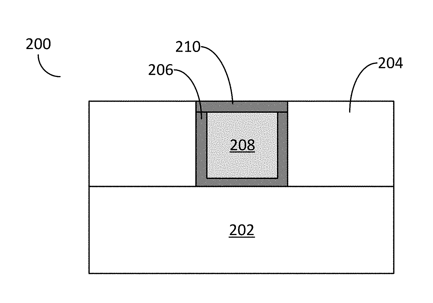
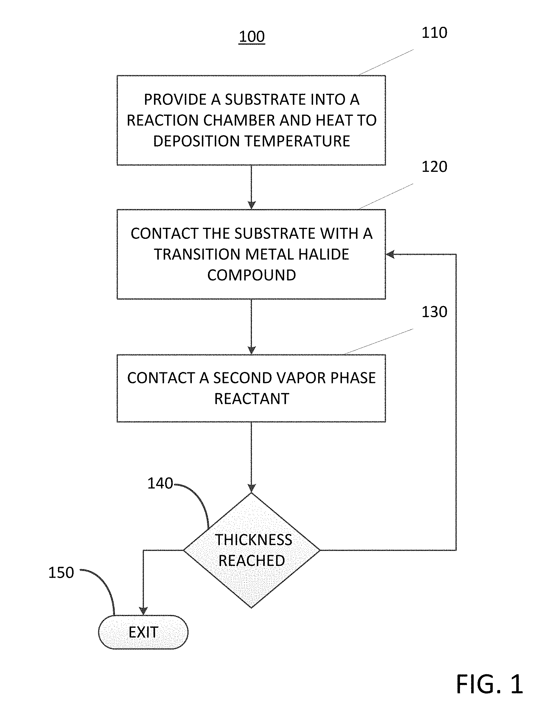
[0016] FIG. 2 illustrates a schematic diagram of an exemplary device structure including a transition metal containing film deposited according to the embodiments of the disclosure;
[0017] FIG. 3 illustrates an example of transition metal halide compound utilized in the cyclical deposition processes of the disclosure;
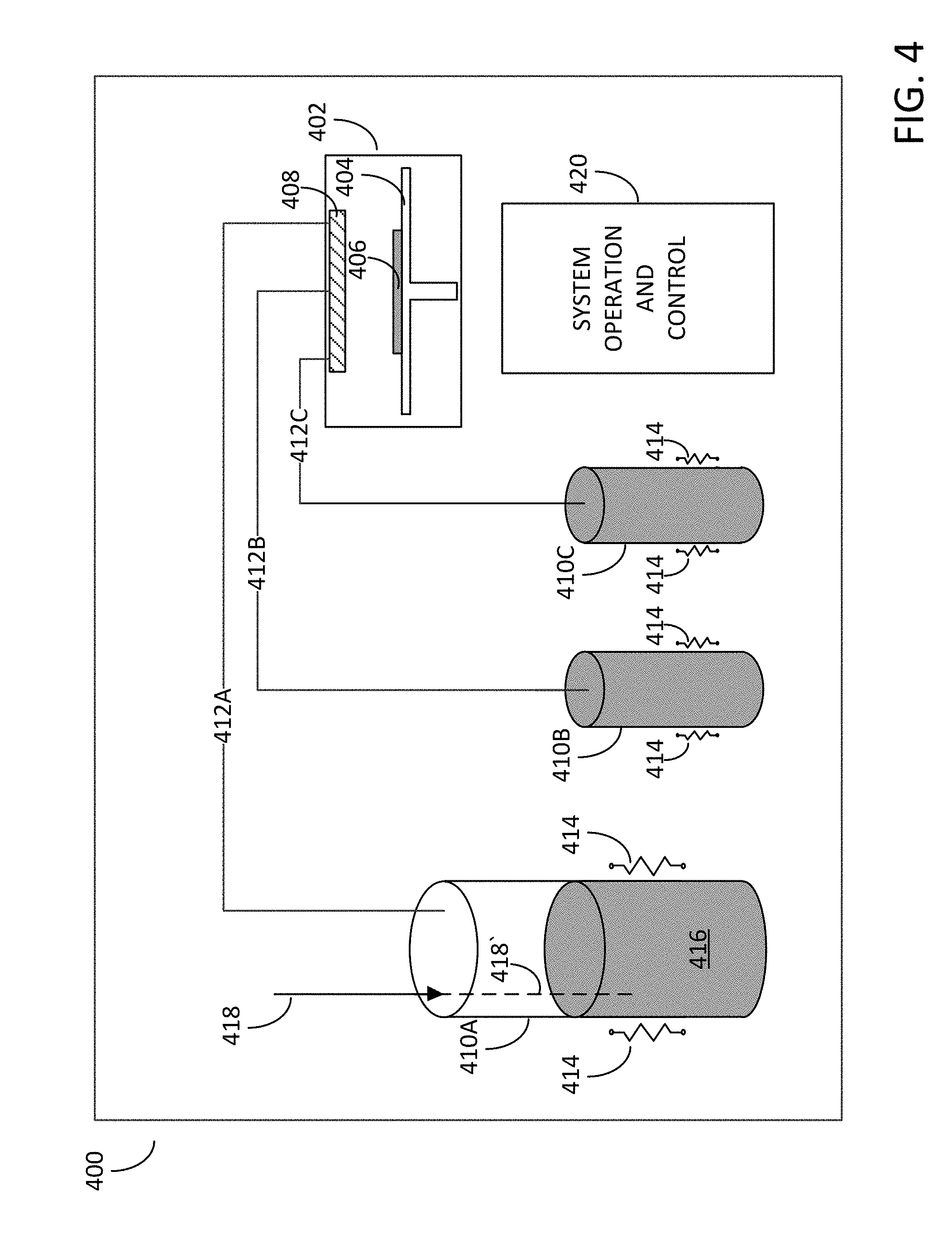
[0018] FIG. 4 illustrates a schematic diagram of an exemplary vapor deposition apparatus according to the embodiments of the disclosure.
DETAILED DESCRIPTION OF EXEMPLARY EMBODIMENTS
[0019] Although certain embodiments and examples are disclosed below, it will be understood by those in the art that the invention extends beyond the specifically disclosed embodiments and/or uses of the invention and obvious modifications and equivalents thereof. Thus, it is intended that the scope of the invention disclosed should not be limited by the particular disclosed embodiments described below.
[0020] The illustrations presented herein are not meant to be actual views of any particular material, structure, or device, but are merely idealized representations that are used to describe embodiments of the disclosure.
[0021] As used herein, the term "cyclic deposition" may refer to the sequential introduction of precursors (reactants) into a reaction chamber to deposit a film over a substrate and includes deposition techniques such as atomic layer deposition and cyclical chemical vapor deposition.
[0022] As used herein, the term "cyclical chemical vapor deposition" may refer to any process wherein a substrate is sequentially exposed to two or more volatile precursors, which react and/or decompose on a substrate to produce a desired deposition.
[0023] As used herein, the term "substrate" may refer to any underlying material or materials that may be used, or upon which, a device, a circuit or a film may be formed.
[0024] As used herein, the term "atomic layer deposition" (ALD) may refer to a vapor deposition process in which deposition cycles, preferably a plurality of consecutive deposition cycles, are conducted in a process chamber. Typically, during each cycle the precursor is chemisorbed to a deposition surface (e.g., a substrate surface or a previously deposited underlying surface such as material from a previous ALD cycle), forming a monolayer or sub-monolayer that does not readily react with additional precursor (i.e., a self-limiting reaction). Thereafter, if necessary, a reactant (e.g., another precursor or reaction gas) may subsequently be introduced into the process chamber for use in converting the chemisorbed precursor to the desired material on the deposition surface. Typically, this reactant is capable of further reaction with the precursor. Further, purging steps may also be utilized during each cycle to remove excess precursor from the process chamber and/or remove excess reactant and/or reaction byproducts from the process chamber after conversion of the chemisorbed precursor. Further, the term "atomic layer deposition," as used herein, is also meant to include processes designated by related terms such as, "chemical vapor atomic layer deposition", "atomic layer epitaxy" (ALE), molecular beam epitaxy (MBE), gas source MBE, or organometallic MBE, and chemical beam epitaxy when performed with alternating pulses of precursor composition(s), reactive gas, and purge (e.g., inert carrier) gas.
[0025] As used herein, the term "film", "thin film", "layer" and "thin layer" may refer to any continuous or non-continuous structures and material deposited by the methods disclosed herein. For example, "film", "thin film", "layer" and "thin layer" could include 2D materials, nanorods, nanotubes, or nanoparticles or even partial or full molecular layers or partial or full atomic layers or clusters of atoms and/or molecules. "Film", "thin film", "layer" and "thin layer" may comprise material or a layer with pinholes, but still be at least partially continuous.
[0026] As used herein, the term "transition metal containing film" may refer to a film containing a transition metal species, including, but not limited to, elemental transition metals, transition metal oxides, transition metal nitrides, transition metal silicides, transition metal selenides, transition metal phosphides, transition metal borides, and mixtures thereof. In addition, the term "transition metal containing film" may refer to a film containing a transition metal species as well as containing carbon and/or hydrogen.
[0027] A number of example materials are given throughout the embodiments of the current disclosure, it should be noted that the chemical formulas given for each of the example materials should not be construed as limiting and that the non-limiting example materials given should not be limited by a given example stoichiometry.
[0028] The present disclosure includes methods for forming transition metal containing films on a substrate and particular methods for the cyclical deposition of a transition metal containing film on a substrate. The embodiments of the disclosure may include methods for the cyclical deposition of transition metal containing films, such as, for example, copper containing films, nickel containing films, and particularly cobalt containing films.
[0029] In particular embodiments of the disclosure, cyclical deposition methods may be utilized to deposit cobalt containing films, such as, for example, elemental cobalt, cobalt oxides, cobalt nitrides, cobalt silicides, cobalt phosphides, cobalt selenides, or cobalt borides. In emerging semiconductor device fabrication processes, cobalt metallic films may be important in such applications as liner layers and capping layers to suppress the electromigration of copper interconnect materials into surrounding dielectric materials. Indeed, as device feature sizes decrease in advanced technology nodes, cobalt metallic films may be utilized as the interconnection material, replacing the commonly utilized copper interconnects. Cobalt metallic films may also be of interest in giant magnetoresistance applications and magnetic memory applications. In addition, cobalt thin films may also be deposited onto silicon gate contacts in integrated circuits to form a cobalt silicide upon annealing. The oxides of cobalt may have applications in emerging energy related technologies, such as, for example, lithium-ion batteries and electrochemical water oxidation, as well as being utilized as a catalysis material.
[0030] Deposition of elemental cobalt and cobalt containing films has been typically achieved utilizing sputtering techniques, as well as CVD methods employing metalorganic precursors. However, such known methods for the deposition of cobalt containing films may be unsuitable for advanced technology nodes due to their inherent non-conformality. Cyclical deposition methods, such as atomic layer deposition, are characteristically conformal deposition methods and are highly suitable for the deposition of conformal transition metal containing films over three-dimensional structure including high aspect ratio features. Accordingly, cyclical deposition methods for the deposition of transition metal containing films, and particular for the deposition of cobalt containing films are highly desirable.
[0031] In addition, the development of cyclical deposition methods for cobalt containing films has been hindered by the lack of suitable chemical precursors and cost effective chemical precursors. For example, the cyclical deposition of cobalt containing films utilizing known chemical precursors may require undesirable high temperature deposition processes, e.g., above 300.degree. C. Plasma enhanced atomic layer deposition processes may be utilized for the deposition of cobalt containing films at lower deposition temperatures but the utilization of a plasma based process may be undesirable in some device applications due to the potential damage of the underlying semiconductor device structures from the high energy plasma reactive species. Accordingly, chemical precursors suitable for the deposition of transition metal containing films are desirable and particular chemical precursor for the deposition of cobalt containing films by cyclical deposition processes. In addition, methods and related apparatus are needed for supplying a chemical precursor to a suitable vapor deposition system, such as, for example, an atomic layer deposition apparatus.
[0032] Therefore, the embodiments of the disclosure may comprise a method of forming a transition metal containing film on a substrate by a cyclical deposition process. The method may comprise: contacting the substrate with a first vapor phase reactant comprising a transition metal halide compound comprising a bidentate nitrogen containing adduct ligand; and contacting the substrate with a second vapor phase reactant.
[0033] In some embodiments of the disclosure, a transition metal containing layer (or film) may be deposited by a cyclical deposition process utilizing a transition metal halide compound as the metal precursor. A non-limiting example embodiment of a cyclical deposition process may include atomic layer deposition (ALD), wherein ALD is based on typically self-limiting reactions, whereby sequential and alternating pulses of reactants are used to deposit about one atomic (or molecular) monolayer of material per deposition cycle. The deposition conditions and precursors are typically selected to provide self-saturating reactions, such that an adsorbed layer of one reactant leaves a surface termination that is non-reactive with the gas phase reactants of the same reactant. The substrate is subsequently contacted with a different reactant that reacts with the previous termination to enable continued deposition. Thus, each cycle of alternated pulses typically leaves no more than about one monolayer of the desired material. However, as mentioned above, the skilled artisan will recognize that in one or more ALD cycles more than one monolayer of material may be deposited, for example if some gas phase reactions occur despite the alternating nature of the process.
[0034] In an ALD-type process for depositing a transition metal containing film, one deposition cycle may comprise, contacting the substrate to a first reactant, removing any unreacted first reactant and reaction byproducts from the reaction space, and contacting the substrate to a second reactant, followed by a second removal step. The first reactant may comprise a transition metal halide compound ("the metal precursor") and the second reactant may comprise at least one of an oxygen precursor, a nitrogen precursor, a silicon precursor, a sulfur precursor, a selenium precursor, a phosphorous precursor, a boron precursor, or a reducing agent.
[0035] Precursors may be separated by inert gases, such as argon (Ar) or nitrogen (N.sub.2), to prevent gas-phase reactions between reactants and enable self-saturating surface reactions. In some embodiments, however, the substrate may be moved to separately contact a first vapor phase reactant and a second vapor phase reactant. Because the reactions self-saturate, strict temperature control of the substrates and precise dosage control of the precursors may not be required. However, the substrate temperature is preferably such that an incident gas species does not condense into monolayers nor decompose on the surface. Surplus chemicals and reaction byproducts, if any, are removed from the substrate surface, such as by purging the reaction space or by moving the substrate, before the substrate is contacted with the next reactive chemical. Undesired gaseous molecules can be effectively expelled from a reaction space with the help of an inert purging gas. A vacuum pump may be used to assist in the purging.
[0036] Reactors capable of being used to deposit transition metal containing films can be used for the deposition. Such reactors include ALD reactors, as well as CVD reactors equipped with appropriate equipment and means for providing the precursors. According to some embodiments, a showerhead reactor may be used. According to some embodiments, cross-flow, batch, minibatch, or spatial ALD reactors may be used.
[0037] Examples of suitable reactors that may be used include commercially available single substrate (or single wafer) deposition equipment such as Pulsar.RTM. reactors (such as the Pulsar.RTM. 2000 and the Pulsar.RTM. 3000 and Pulsar.RTM. XP ALD), and EmerALD.RTM. XP and the EmerALD.RTM. reactors, available from ASM America, Inc. of Phoenix, Ariz. and ASM Europe B.V., Almere, Netherlands. Other commercially available reactors include those from ASM Japan K.K. (Tokyo, Japan) under the tradename Eagle.RTM. XP and XP8. In some embodiments, the reactor is a spatial ALD reactor, in which the substrates moves or rotates during processing.
[0038] In some embodiments of the disclosure a batch reactor may be used. Suitable batch reactors include, but are not limited to, Advance.RTM. 400 Series reactors commercially available from and ASM Europe B.V. (Almere, Netherlands) under the trade names A400 and A412 PLUS. In some embodiments the wafers rotate during processing. In other embodiments, the batch reactor comprises a minibatch reactor configured to accommodate 10 or fewer wafers, 8 or fewer wafers, 6 or fewer wafers, 4 or fewer wafers, or 2 or fewer wafers. In some embodiments in which a batch reactor is used, wafer-to-wafer non-uniformity is less than 3% (1sigma), less than 2%, less than 1% or even less than 0.5%.
[0039] The deposition processes described herein can optionally be carried out in a reactor or a reaction chamber connected to a cluster tool. In a cluster tool, because each reaction chamber is dedicated to one type of process, the temperature of the reaction chamber in each module can be kept constant, which improves the throughput compared to a reactor in which the substrate is heated up to the process temperature before each run. Additionally, in a cluster tool it is possible to reduce the time to pump the reaction chamber to the desired process pressure levels between substrates. In some embodiments of the disclosure, the deposition process may be performed in a cluster tool comprising multiple reaction chambers, wherein each individual reaction chamber may be utilized to expose the substrate to an individual precursor gas and the substrate may be transferred between the different reaction chambers for exposure to multiple precursors gases, the transfer of the substrate being performed under a controlled ambient to prevent oxidation/contamination of the substrate. In some embodiments of the disclosure, the deposition process may be performed in a cluster tool comprising multiple reaction chambers, wherein each individual reaction chamber may be configured to heat the substrate to a different deposition temperature.
[0040] A stand-alone reactor can be equipped with a load-lock. In that case, it is not necessary to cool down the reaction space between each run. In some embodiments a deposition process for depositing a transition metal containing film may comprise a plurality of deposition cycles, for example ALD cycles, or cyclical CVD cycles.
[0041] In some embodiments the cyclical deposition processes are used to form transition metal containing films on a substrate and the cyclical deposition process may be an ALD type process. In some embodiments the cyclical deposition may be a hybrid ALD/CVD or cyclical CVD process. For example, in some embodiments the growth rate of the ALD process may be low compared with a CVD process. One approach to increase the growth rate may be that of operating at a higher substrate temperature than that typically employed in an ALD process, resulting in a chemical vapor deposition process, but still taking advantage of the sequential introduction of precursors, such a process may be referred to as cyclical CVD.
[0042] According to some embodiments of the disclosure, ALD processes may be used to deposit a transition metal containing film on a substrate, such as a partially fabricated semiconductor device structure. In some embodiments of the disclosure each ALD cycle comprises two distinct deposition steps or phases. In a first phase of the deposition cycle ("the metal phase"), the substrate surface on which deposition is desired is contacted with a first vapor phase reactant comprising a metal precursor which chemisorbs onto the substrate surface, forming no more than about one monolayer of reactant species on the surface of the substrate. In a second phase of the deposition, the substrate surface on which deposition is desired is contacted with a second vapor phase reactant comprising at least one of an oxygen precursor, a nitrogen precursor, a silicon precursor, a sulfur precursor, a selenium precursor, a phosphorous precursor, a boron precursor, or a reducing agent, wherein the second vapor phase reactant may react with transition metal species on a surface of the substrate to form a transition metal containing film on the substrate, such as, for example, an elemental transition metal, a transition metal oxide, a transition metal nitride, a transition metal silicide, a transition metal selenide, a transition metal phosphide, a transition metal boride, and mixtures thereof, as well transition metal containing films further comprising carbon and/or hydrogen.
[0043] In some embodiments of the disclosure, the first vapor phase reactant may comprise a metal containing precursor, also referred to here as the "metal compound". In some embodiments, the first vapor phase reactant may comprise a transition metal compound with an adduct forming ligand. In some embodiments, the first vapor phase reactant may comprise a transition metal compound. In some embodiments, the first vapor phase reactant may comprise a transition metal halide compound. In some embodiments, the first vapor phase reactant may comprise a transition metal compound with an adduct forming ligand, such as monodentate, bidentate, or multidentate adduct forming ligand. In some embodiments, the first vapor phase reactant may comprise a transition metal halide compound with adduct forming ligand, such as monodentate, bidentate, or multidentate adduct forming ligand. In some embodiments, the first vapor phase reactant may comprise a transition metal compound with adduct forming ligand comprising nitrogen, such as monodentate, bidentate, or multidentate adduct forming ligand comprising nitrogen. In some embodiments, the first vapor phase reactant may comprise a transition metal compound with adduct forming ligand comprising phosphorous, oxygen, or sulfur, such as monodentate, bidentate, or multidentate adduct forming ligand comprising phosphorous, oxygen or sulfur. For example, in some embodiments, the transition metal halide compound may comprise a transition metal chloride, a transition metal iodide, a transition metal fluoride, or a transition metal bromide. In some embodiments of the disclosure, the transition metal halide compound may comprise a transition metal species, including, but not limited to, at least one of cobalt, nickel, or copper. In some embodiments of the disclosure, the transition metal halide compound may comprise at least one of a cobalt chloride, a nickel chloride, or a copper chloride. In some embodiments, the transition metal halide compound may comprise a bidentate nitrogen containing adduct forming ligand. In some embodiment, the transition metal halide compound may comprise an adduct forming ligand including two nitrogen atoms, wherein each of the nitrogen atoms are bonded to at least one carbon atom. In some embodiments of the disclosure, the transition metal halide compound comprises one or more nitrogen atoms bonded to a central transition metal atom thereby forming a metal complex.
[0044] In some embodiments of the disclosure, the first vapor phase reactant may comprise a transition metal compound having the formula (I):
(adduct).sub.n-M-X.sub.a (I)
[0045] wherein each of the "adducts" is an adduct forming ligand and can be independently selected to be a mono-, a bi-, or a multidentate adduct forming ligand or mixtures thereof: n is from 1 to 4 in case of monodentate forming ligand, n is from 1 to 2 in case of bi- or multidentate adduct forming ligand; M is a transition metal, such as, for example, cobalt (Co), copper (Cu), or nickel (Ni); wherein each of X.sub.a is another ligand, and can be independently selected to be a halide or other ligand; wherein a is from 1 to 4, and some instances a is 2.
[0046] In some embodiments of the disclosure, the adduct forming ligand in the transition metal compound, such as a transition metal halide compound, may comprise a monodentate, bidentate, or multidentate adduct forming ligand which coordinates to the transition metal atom, of the transition metal compound, through at least one of a nitrogen atom, a phosphorous atom, an oxygen atom, or a sulfur atom. In some embodiments of the disclosure, the adduct forming ligand in the transition metal compound may comprise a cyclic adduct ligand. In some embodiments of the disclosure, the adduct forming ligand in the transition metal compound may comprise mono, di-, or polyamines. In some embodiments of the disclosure, the adduct forming ligand in the transition metal compound may comprise mono-, di-, or polyethers. In some embodiments, the adduct forming ligand in the transition metal compound may comprise mono-, di-, or polyphosphines. In some embodiments, the adduct forming ligand in the transition metal compound may comprise carbon and/or in addition to the nitrogen, oxygen, phosphorous, or sulfur in the adduct forming ligand.
[0047] In some embodiments of the disclosure, the adduct forming ligand in the transition metal compound may comprise one monodentate adduct forming ligand. In some embodiments of the disclosure, the adduct forming ligand in the transition metal compound may comprise two monodentate adduct forming ligands. In some embodiments of the disclosure, the adduct forming ligand in the transition metal compound may comprise three monodentate adduct forming ligand. In some embodiments of the disclosure, the adduct forming ligand in the transition metal compound may comprise four monodentate adduct forming ligands. In some embodiments of the disclosure, the adduct forming ligand in the transition metal compound may comprise one bidentate adduct forming ligand. In some embodiments of the disclosure, the adduct forming ligand in the transition metal compound may comprise two bidentate adduct forming ligands. In some embodiments of the disclosure, the adduct forming ligand in the transition metal compound may comprise one multidentate adduct forming ligand. In some embodiments of the disclosure, the adduct forming ligand in the transition metal compound may comprise two multidentate adduct forming ligands.
[0048] In some embodiments of the disclosure, the adduct forming ligand comprises nitrogen, such as an amine, a diamine, or a polyamine adduct forming ligand. In such embodiments, the transition metal compound may comprise at least one of, triethylamine (TEA), N,N,N',N'-tetramethyl-1,2-ethylenediamine (CAS: 110-18-9) (TMEDA), N,N,N',N'-Tetraethylethylenediamine (CAS: 150-77-6) (TEEDA), N,N'-diethyl-1,2-ethylenediamine (CAS: 111-74-0) (DEEDA), N,N'-diisopropylethylenediamine (CAS: 4013-94-9), N,N,N',N'-tetramethyl-1,3-propanediamine (CAS: 110-95-2) (TMPDA), N,N,N',N'-tetramethylmethanediamine (CAS: 51-80-9) (TMMDA), N,N,N',N'',N''-pentamethyldiethylenetriamine (CAS: 3030-47-5) (PMDETA), diethylenetriamine (CAS: 111-40-0) (DIEN), triethylenetetraamine (CAS: 112-24-3) (TRIEN), Tris(2-aminoethyl)amine (CAS: 4097-89-6) (TREN, TAEA), 1,1,4,7,10,10-Hexamethyltriethylenetetramine (CAS: 3083-10-1) (HMTETA), 1,4,8,11-Tetraazacyclotetradecane (CAS: 295-37-4) (Cyclam), 1,4,7-Trimethyl-1,4,7-triazacyclononane (CAS: 96556-05-7), or 1,4,8,11-Tetramethyl-1,4,8,11-tetraazacyclotetradecane (CAS: 41203-22-9).
[0049] In some embodiments of the disclosure, the adduct forming ligand comprises phosphorous, such as a phosphine, a diphosphine, or a polyphosphine adduct forming ligand. For example the transition metal compound may comprise at least one of, triethylphosphine (CAS: 554-70-1), trimethyl phosphite (CAS: 121-45-), 1,2-Bis(diethylphosphino)ethane (CAS: 6411-21-8) (BDEPE), or 1,3-Bis(diethylphosphino)propane (CAS: 29149-93-7).
[0050] In some embodiments of the disclosure, the adduct forming ligand comprises oxygen, such as an ether, a diether, or a polyether adduct forming ligand. For example, the transition metal compound may comprise at least one of, 1,4-dioxane (CAS: 123-91-1), 1,2-dimethoxyethane (CAS: 110-71-4) (DME, monoglyme), Diethylene glycol dimethyl ether (CAS: 111-96-6) (diglyme), Triethylene glycol dimethyl ether (CAS: 112-49-2) (triglyme), or 1,4,7,10-Tetraoxacyclododecane (CAS: 294-93-9) (12-Crown-4).
[0051] In some embodiments of the disclosure, the adduct forming ligand may comprise a thiother, or mixed ether amine, such as, for example, at least one of 1,7-Diaza-12-crown-4: 1,7-Dioxa-4,10-diazacyclododecane (CAS: 294-92-8), or 1,2-bis(methylthio)ethane (CAS: 6628-18-8).
[0052] In some embodiments, the transition metal halide compound may comprise cobalt chloride N,N,N',N'-tetramethyl-1,2-ethylenediamine (CoCl.sub.2(TMEDA)). In some embodiments, the transition metal halide compound may comprise cobalt bromide tetramethylethylenediamine (CoBr.sub.2(TMEDA)). In some embodiments, the transition metal halide compound may comprise cobalt iodide tetramethylethylenediamine (CoI.sub.2(TMEDA)). In some embodiments, the transition metal halide compound may comprise cobalt chloride N,N,N',N'-tetramethyl-1,3-propanediamine (CoCl.sub.2(TMPDA)). In some embodiments of the disclosure, the transition metal halide compound may comprise at least one of cobalt chloride N,N,N',N'-tetramethyl-1,2-ethylenediamine (CoCl.sub.2(TMEDA)), nickel chloride tetramethyl-1,3-propanediamine (NiCl.sub.2(TMPDA)), or nickel iodide tetramethyl-1,3-propanediamine (NiI.sub.2(TMPDA)).
[0053] In some embodiments of the disclosure, contacting the substrate with a first vapor phase reactant comprising a transition metal halide compound, i.e., the transition metal halide comprising an adduct forming ligand, may comprise exposing, i.e., contacting, the substrate to the transition metal halide compound for a time period of between about 0.01 seconds and about 60 seconds, between about 0.05 seconds and about 10 seconds, or between about 0.1 seconds and about 5.0 seconds. In addition, during the pulsing of the transition metal halide compound, the flow rate of the transition metal halide compound may be less than 2000 sccm, or less than 500 sccm, or even less than 100 sccm. In addition, during the pulsing of the transition metal halide compound over the substrate the flow rate of the transition metal halide compound may range from about 1 to 2000 sccm, from about 5 to 1000 sccm, or from about 10 to about 500 sccm.
[0054] Excess transition metal halide compound and reaction byproducts (if any) may be removed from the surface, e.g., by pumping with an inert gas. For example, in some embodiments of the disclosure, the methods may comprise a purge cycle wherein the substrate surface is purged for a time period of less than approximately 2.0 seconds. Excess transition metal halide compound and any reaction byproducts may be removed with the aid of a vacuum, generated by a pumping system, in fluid communication with the reaction chamber.
[0055] In a second phase of the deposition cycle the substrate may be contacted with a second vapor phase reactant comprising at least one of an oxygen precursor, a nitrogen precursor, a silicon precursor, a sulfur precursor, a selenium precursor, a phosphorous precursor, a boron precursor, or a reducing agent. In some embodiments, the second vapor phase reactant may comprise an oxygen precursor and the transition metal containing film deposited by the cyclical deposition methods disclosed herein may comprise a transition metal oxide. In some embodiments, the second vapor phase reactant may comprise a reducing agent, described in greater detail below, and the transition metal containing film deposited by the cyclical deposition methods disclosed here may comprise an elemental transition metal. In some embodiments, the second vapor phase reactant may comprise a nitrogen precursor and the transition metal containing film deposited by the cyclical deposition methods disclosed herein may comprise a transition metal nitride. In some embodiments, the second vapor phase reactant may comprise a silicon precursor and the transition metal containing film deposited by the cyclical deposition methods disclosed herein may comprise a transition metal silicide. In some embodiments, the second vapor phase reactant may comprise a sulfur precursor and the transition metal containing film deposited by the cyclical deposition methods disclosed herein may comprise a transition metal sulfide. In some embodiments, the second vapor phase reactant may comprise a selenium precursor and the transition metal containing film deposited by the cyclical deposition methods disclosed herein may comprise a transition metal selenide. In some embodiments, the second vapor phase reactant may comprise a phosphorous precursor and the transition metal containing film deposited by the cyclical deposition methods disclosed herein may comprise a transition metal phosphide. In some embodiments, the second vapor phase reactant may comprise a boron precursor and the transition metal containing film deposited by the cyclical deposition methods disclosed herein may comprise a transition metal boride.
[0056] In embodiments of the disclosure wherein the second vapor phase reactant comprises an oxygen precursor, the oxygen precursor may comprise at least one of ozone (O.sub.3), molecular oxygen (O.sub.2), oxygen atoms (O), an oxygen plasma, oxygen radicals, oxygen excited species, water (H.sub.2O), or hydrogen peroxide (H.sub.2O.sub.2).
[0057] In embodiments of the disclosure wherein the second vapor phase reactant comprises a nitrogen precursor, the nitrogen precursor may comprise at least one of ammonia (NH.sub.3), hydrazine (N.sub.2H.sub.4), triazane (N.sub.3H.sub.5), tertbutylhydrazine (C.sub.4H.sub.9N.sub.2H.sub.3), methylhydrazine (CH.sub.3NHNH.sub.2), dimethylhydrazine ((CH.sub.3).sub.2N.sub.2H.sub.2), or a nitrogen plasma or nitrogen plasma comprising hydrogen.
[0058] In some embodiments the second vapor phase reactant may comprise a hydrocarbon substituted hydrazine precursor. In a second phase of the deposition cycle ("substituted hydrazine phase"), the substrate is contacted with a second vapor phase reactant comprising a hydrocarbon substituted hydrazine precursor. In some embodiments of the disclosure, methods may further comprise selecting the substituted hydrazine to comprise an alkyl group with at least four (4) carbon atoms, wherein "alkyl group" refers to a saturated or unsaturated hydrocarbon chain of at least four (4) carbon atoms in length, such as, but not limited to, butyl, pentyl, hexyl, heptyl and octyl and isomers thereof, such as n-, iso-, sec- and tert-isomers of those. The alkyl group may be straight chain or branched-chain and may embrace all structural isomer forms of the alkyl group. In some embodiments the alkyl chain might be substituted. In some embodiments of the disclosure, the alkyl-hydrazine may comprise at least one hydrogen bonded to nitrogen. In some embodiments of the disclosure, the alkyl-hydrazine may comprise at least two hydrogens bonded to nitrogen. In some embodiments of the disclosure, the alkyl-hydrazine may comprise at least one hydrogen bonded to nitrogen and at least one alkyl chain bonded to nitrogen. In some embodiments of the disclosure, the second reactant may comprise an alkyl-hydrazine and may further comprise one or more of tertbutylhydrazine (C.sub.4H.sub.9N.sub.2H.sub.3), dimethylhydrazine or diethylhydrazine. In some embodiments of the disclosure, the substituted hydrazine has at least one hydrocarbon group attached to nitrogen. In some embodiments of the disclosure, the substituted hydrazine has at least two hydrocarbon groups attached to nitrogen. In some embodiments of the disclosure, the substituted hydrazine has at least three hydrocarbon groups attached to nitrogen. In some embodiments of the disclosure, the substituted hydrazine has at least one C1-C3 hydrocarbon group attached to nitrogen. In some embodiments of the disclosure, the substituted hydrazine has at least one C4-C10 hydrocarbon group attached to nitrogen. In some embodiments of the disclosure, the substituted hydrazine has linear, branched or cyclic or aromatic hydrocarbon group attached to nitrogen. In some embodiments of the disclosure the substituted hydrazine comprises substituted hydrocarbon group attached to nitrogen.
[0059] In some embodiments of the disclosure, the substituted hydrazine has the following formula II:
R.sup.IR.sup.II--N--NR.sup.IIIR.sup.IV, (II)
[0060] wherein R.sup.1 can be selected from hydrocarbon group, such as linear, branched, cyclic, aromatic or substituted hydrocarbon group and each of the R.sup.II, R.sup.III, R.sup.IV groups can be independently selected to be hydrogen or hydrocarbon groups, such as linear, branched, cyclic, aromatic or substituted hydrocarbon group.
[0061] In some embodiments in the formula (II) each of the R.sup.I, R.sup.II, R.sup.III, R.sup.IV can be C1-C10 hydrocarbon, C1-C3 hydrocarbon, C4-C10 hydrocarbon or hydrogen, such as linear, branched, cyclic, aromatic or substituted hydrocarbon group. In some embodiments at least one of the R.sup.I, R.sup.II, R.sup.III, R.sup.IV groups comprises aromatic group such as phenyl group. In some embodiments at least one of the R.sup.I, R.sup.II, R.sup.III, R.sup.IV groups comprises methyl, ethyl, n-propyl, i-propyl, n-butyl, i-butyl, s-butyl, tertbutyl group or phenyl group. In some embodiments at least two of the each R.sup.I, R.sup.II, R.sup.III, R.sup.IV groups can be independently selected to comprise methyl, ethyl, n-propyl, i-propyl, n-butyl, i-butyl, s-butyl, tertbutyl group or phenyl group. In some embodiments R.sup.II, R.sup.III and R.sup.IV groups are hydrogen. In some embodiments at least two one of the R.sup.II, R.sup.III, R.sup.IV groups are hydrogen. In some embodiments at least one of the R.sup.II, R.sup.III, R.sup.IV groups are hydrogen. In some embodiments all of the R.sup.II, R.sup.III, R.sup.IV groups are hydrocarbons.
[0062] In embodiments of the disclosure wherein the second vapor phase reactant comprises a silicon precursor, the silicon precursor may comprise at least one of silane (SiH.sub.4), disilane (Si.sub.2H.sub.6), trisilane (Si.sub.3H.sub.8), tetrasilane (Si.sub.4H.sub.10), isopentasilane (Si.sub.5H.sub.12), or neopentasilane (Si.sub.5H.sub.12). In embodiments of the disclosure wherein the second vapor phase reactant comprises a silicon precursor, the silicon precursor may comprise a C1-C4 alkylsilane. In embodiments of the disclosure wherein the second vapor phase reactant comprises a silicon precursor, the silicon precursor may comprise a precursor from silane family.
[0063] In embodiments of the disclosure wherein the second vapor phase reactant comprises a boron precursor, the boron precursor may comprise at least one of borane (BH.sub.3), diborane (B.sub.2H.sub.6) or other boranes, such as decaborane (B.sub.10H.sub.14).
[0064] In embodiments of the disclosure wherein the second vapor phase reactant comprises a hydrogen precursor, the hydrogen precursor may comprise at least one of H.sub.2, H atoms, H-ions, H-plasma or H-radicals.
[0065] In some embodiments of the disclosure, the second vapor phase reactant comprises a phosphorus precursor, a sulfur precursor, or a selenide precursor. In some embodiments the sulfur precursor comprises hydrogen and sulfur. In some embodiments the sulfur precursor is an alkylsulfur compound. In some embodiments the second reactant comprises one or more of elemental sulfur, H.sub.2S, (CH.sub.3).sub.2S, (NH.sub.4).sub.2S, ((CH.sub.3).sub.2SO), and H.sub.2S.sub.2. In some embodiments the selenium precursor is an alkylselenium compound. In some embodiments the second reactant comprises one or more of elemental selenium, H.sub.2Se, (CH.sub.3).sub.2Se and H.sub.2Se.sub.2. In some embodiments the selenium precursor comprises hydrogen and selenium. In some embodiment, the second reactant may comprise alkylsilylcompounds of Te, Sb, Se, such as (Me3Si)2Te, (Me3Si)2Se or (Me3Si)3Sb. In some embodiments the phosphorus precursor is an alkylphosphorus compound. In some embodiments the second reactant comprises one or more of elemental phosphorus, PH.sub.3 or alkylphosphines, such as methylphoshpine. In some embodiments the phosphorus precursor comprises hydrogen and phosphorus.
[0066] In embodiments of the disclosure wherein the second vapor phase reactant comprises an organic precursor, such as a reducing agent, for example, alcohols, aldehydes or carboxylic acids or other organic compounds may be utilized, For example organic compounds not having metals or semimetals, but comprising --OH group. Alcohols can be primary alcohols, secondary alcohols, tertiary alcohols, polyhydroxy alcohols, cyclic alcohols, aromatic alcohols, and other derivatives of alcohols.
[0067] Primary alcohols have an --OH group attached to a carbon atom which is bonded to another carbon atom, in particular primary alcohols according to the general formula (III):
R1-OH (III)
[0068] wherein R1 is a linear or branched C1-C20 alkyl or alkenyl groups, such as methyl, ethyl, propyl, butyl, pentyl or hexyl. Examples of primary alcohols include methanol, ethanol, propanol, butanol, 2-methyl propanol and 2-methyl butanol.
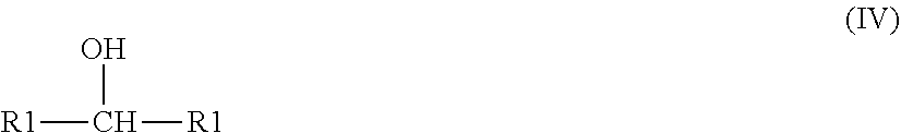
[0069] Secondary alcohols have an --OH group attached to a carbon atom that is bonded to two other carbon atoms. In particular, secondary alcohols have the general formula (IV):
##STR00001##
[0070] wherein each R1 is selected independently from the group of linear or branched C1-C20 alkyl and alkenyl groups, such as methyl, ethyl, propyl, butyl, pentyl or hexyl. Examples of secondary alcohols include 2-propanol and 2-butanol.
[0071] Tertiary alcohols have an --OH group attached to a carbon atom that is bonded to three other carbon atoms. In particular, tertiary alcohols have the general formula (V):
##STR00002##
[0072] wherein each R1 is selected independently from the group of linear or branched C1-C20 alkyl and alkenyl groups, such as methyl, ethyl, propyl, butyl, pentyl or hexyl. An example of a tertiary alcohol is tert-butanol.
[0073] Polyhydroxy alcohols, such as diols and triols, have primary, secondary and/or tertiary alcohol groups as described above. Examples of polyhydroxy alcohol are ethylene glycol and glycerol.
[0074] Cyclic alcohols have an --OH group attached to at least one carbon atom which is part of a ring of 1 to 10, such as 5-6 carbon atoms.
[0075] Aromatic alcohols have at least one --OH group attached either to a benzene ring or to a carbon atom in a side chain.
[0076] Organic precursors may comprise at least one aldehyde group (--CHO) are selected from the group consisting of compounds having the general formula (VI), alkanedial compounds having the general formula (VII), halogenated aldehydes and other derivatives of aldehydes.
[0077] Thus, in one embodiment organic precursors are aldehydes having the general formula (VI):
R3-CHO (VI)
[0078] wherein R3 is selected from the group consisting of hydrogen and linear or branched C1-C20 alkyl and alkenyl groups, such as methyl, ethyl, propyl, butyl, pentyl or hexyl. In some embodiments, R3 is selected from the group consisting of methyl or ethyl. Exemplary compounds, but not limited to, according to formula (VI) are formaldehyde, acetaldehyde and butyraldehyde.
[0079] In another embodiment organic precursors are aldehydes having the general formula (VII):
[0080] OHC--R4-CHO (VII) wherein R4 is a linear or branched C1-C20 saturated or unsaturated hydrocarbon. Alternatively, the aldehyde groups may be directly bonded to each other (R4 is null).
[0081] Organic precursors containing at least one --COOH group can be selected from the group consisting of compounds of the general formula (VIII), polycarboxylic acids, halogenated carboxylic acids and other derivatives of carboxylic acids.
[0082] Thus, in one embodiment organic precursors are carboxylic acids having the general formula (VIII):
R5-COOH (VIII)
[0083] wherein R5 is hydrogen or linear or branched C1-C20 alkyl or alkenyl group, such as methyl, ethyl, propyl, butyl, pentyl or hexyl, for example methyl or ethyl. In some embodiments, R5 is a linear or branched C1-C3 alkyl or alkenyl group. Examples of compounds according to formula (VII) are formic acid, propanoic acid and acetic acid, in some embodiments formic acid (HCOOH).
[0084] In some embodiments of the disclosure, exposing, i.e., contacting, the substrate to the second vapor phase reactant comprise pulsing the second vapor phase reactant over the substrate for a time period of between 0.1 seconds and 2.0 seconds, or from about 0.01 seconds to about 10 seconds, or less than about 20 seconds, less than about 10 seconds or less than about 5 seconds. During the pulsing of the second vapor phase reactant over the substrate the flow rate of the second vapor phase reactant may be less than 50 sccm, or less than 25 sccm, or less than 15 sccm, or even less than 10 sccm.
[0085] Excess second vapor phase reactant and reaction byproducts, if any, may be removed from the substrate surface, for example, by a purging gas pulse and/or vacuum generated by a pumping system. Purging gas is preferably any inert gas, such as, without limitation, argon (Ar), nitrogen (N.sub.2), helium (He), or in some instances hydrogen (H.sub.2) could be used. A phase is generally considered to immediately follow another phase if a purge (i.e., purging gas pulse) or other reactant removal step intervenes.
[0086] A deposition cycle in which the substrate is alternatively contacted with the first vapor phase reactant (i.e., the metal halide compound) and the second vapor phase reactant (e.g., an oxygen precursor) may be repeated one or more times until a desired thickness of a transition metal containing film is deposited. It should be appreciated that in some embodiments of the disclosure, the order of the contacting of the substrate with the first vapor phase reactant and the second vapor phase reactant may be such that the substrate is first contacted with the second vapor phase reactant followed by the first vapor phase reactant. In addition, in some embodiments, the cyclical deposition process may comprise contacting the substrate with the first vapor phase reactant one or more times prior to contacting the substrate with the second vapor phase reactant one or more times and similarly may alternatively comprise contacting the substrate with the second vapor phase reactant one or more times prior to contacting the substrate with the first vapor phase reactant one or more times.
[0087] In addition, some embodiments of the disclosure may comprise non-plasma reactants, e.g., the first and second vapor phase reactants are substantially free of ionized reactive species. In some embodiments, the first and second vapor phase reactants are substantially free of ionized reactive species, excited species or radical species. For example, both the first vapor phase reactant and the second vapor phase reactant may comprise non-plasma reactants to prevent ionization damage to the underlying substrate and the associated defects thereby created. The use of non-plasma reactants may be especially useful when the underlying substrate contains fragile fabricated, or least partially fabricated, semiconductor device structures as the high energy plasma species may damage and/or deteriorate device performance characteristics.
[0088] In some embodiments of the disclosure, exemplary cyclical deposition methods of the disclosure may comprise an additional process step comprising, contacting the substrate with a third vapor phase reactant comprising a reducing agent. In some embodiments, the reducing agent may comprise at least one of hydrogen (H.sub.2), a hydrogen (H.sub.2) plasma, ammonia (NH.sub.3), an ammonia (NH.sub.3) plasma, hydrazine (N.sub.2H.sub.4), silane (SiH.sub.4), disilane (Si.sub.2H.sub.6), trisilane (Si.sub.3H.sub.8), germane (GeH.sub.4), digermane (Ge.sub.2H.sub.6), borane (BH.sub.3), diborane (B.sub.2H.sub.6), tertiary butyl hydrazine (C.sub.4H.sub.12N.sub.2, a selenium precursor, a boron precursor, a phosphorous precursor, a sulfur precursor, an organic precursor (e.g., alcohols, aldehydes, or carboxylic acids) or a hydrogen precursor. In some embodiments of the disclosure, exemplary cyclical deposition methods of the disclosure may comprise contacting the substrate with a second vapor phase reactant which is a reducing agent (without any additional precursor/reactant contacting steps).
[0089] The third vapor phase reactant comprising a reducing agent may be introduced into the reaction chamber and contact the substrate at a number process stages in an exemplary cyclical deposition method. In some embodiments of the disclosure, the reducing agent may be introduced into the reaction chamber and contact the substrate separately from the first vapor phase reactant and separately from the second vapor phase reactant. For example, the reducing agent may be introduced into the reaction chamber and contact the substrate prior to contacting the substrate with the first vapor phase reactant, after contacting the substrate with the first vapor phase reactant and prior to contacting the substrate with the second vapor phase reactant, and/or after contacting the substrate with the second vapor phase reactant. In some embodiments of the disclosure, the reducing agent may be introduced into the reaction chamber and contact the substrate simultaneously with the first vapor phase reactant and/or simultaneously with the second vapor phase reactant. For example, the reducing agent and the first vapor phase reactant may be co-flowed into the reaction chamber and simultaneously contact the substrate, and/or the reducing agent and the second vapor phase reactant may be co-flowed into the reaction chamber and simultaneously contact the substrate.
[0090] In some embodiments of the disclosure, the first vapor phase reactant may comprise a transition metal halide compound and the second vapor phase reactant may comprise an oxygen precursor. In such embodiments, the cyclical deposition processes may deposit a transition metal oxide on the substrate. As a non-limiting example, the first vapor phase reactant may comprise CoCl.sub.2(TMEDA), the second vapor phase reactant may comprise water (H.sub.2O), and the film deposited on the substrate may comprise a cobalt oxide. In some embodiments, the transition metal oxide may be further processed by exposing the transition metal oxide to a reducing agent. In some embodiments, the transition metal oxide may be exposed to at least one reducing agent comprising, forming gas (H.sub.2+N.sub.2), ammonia (NH.sub.3), hydrazine (N.sub.2H.sub.4), molecular hydrogen (H.sub.2), hydrogen atoms (H), a hydrogen plasma, hydrogen radicals, hydrogen excited species, alcohols, aldehydes, carboxylic acids, boranes, or amines.
[0091] In some embodiments, exposing the transition metal oxide to a reducing agent may reduce the transition metal oxide to an elemental transition metal. As a non-limiting example, the cyclical deposition processes of the disclosure may be utilized to deposit a cobalt oxide film to a thickness of 50 nanometers and the cobalt oxide film may be exposed to 10% forming gas at a pressure of 1000 mbar and a temperature of approximately 250.degree. C. to reduce the cobalt oxide film to elemental cobalt. In some embodiments of the disclosure, the transition metal oxide may have a thickness of less than 500 nanometers, or less than 100 nanometers, or less than 50 nanometers, or less than 25 nanometers, or less than 20 nanometers, or less than 10 nanometers, or even less than 5 nanometers. In some embodiments, the transition metal oxide may be exposed to a reducing agent for less than 5 hours, or less than 1 hour, or less than 30 minutes, or less than 15 minutes, or less than 10 minutes, or less than 5 minutes, or even less than 1 minutes. In some embodiments, the transition metal oxide may be exposed to the reducing agent at a substrate temperature of less than 500.degree. C., or less than 400.degree. C., or less than 300.degree. C., or less than 250.degree. C., or less than 200.degree. C., or even less than 150.degree. C. In some embodiments, the transition metal oxide may be exposed to the reducing agent in a reduced pressure atmosphere, wherein the pressure may be from about 0.001 mbar to about 10 bar, or from about 1 mbar to about 1000 mbar.
[0092] The cyclical deposition processes described herein, utilizing a first vapor phase reactant comprise a transition metal halide compound and a second vapor phase reactant to deposit a transition metal containing film, may be performed in an ALD or CVD deposition system with a heated substrate. For example, in some embodiments, methods may comprise heating the substrate to temperature of between approximately 80.degree. C. and approximately 150.degree. C., or even heating the substrate to a temperature of between approximately 80.degree. C. and approximately 120.degree. C. Of course, the appropriate temperature window for any given cyclical deposition process, such as, for an ALD reaction, will depend upon the surface termination and reactant species involved. Here, the temperature varies depending on the precursors being used and is generally at or below about 700.degree. C. In some embodiments, the deposition temperature is generally at or above about 100.degree. C. for vapor deposition processes, in some embodiments the deposition temperature is between about 100.degree. C. and about 300.degree. C., and in some embodiments the deposition temperature is between about 120.degree. C. and about 200.degree. C. In some embodiments the deposition temperature is less than about 500.degree. C., or less than below about 400.degree. C., or less than about 350.degree. C., or below about 300.degree. C. In some instances the deposition temperature can be below about 300.degree. C., below about 200.degree. C. or below about 100.degree. C. In some instances the deposition temperature can be above about 20.degree. C., above about 50.degree. C. and above about 75.degree. C. In some embodiments of the disclosure, the deposition temperature i.e., the temperature of the substrate during deposition is approximately 275.degree. C.
[0093] In some embodiments, the growth rate of the transition metal containing film is from about 0.005 .ANG./cycle to about 5 .ANG./cycle, from about 0.01 .ANG./cycle to about 2.0 .ANG./cycle. In some embodiments the growth rate of the transition metal containing film is more than about 0.05 .ANG./cycle, more than about 0.1 .ANG./cycle, more than about 0.15 .ANG./cycle, more than about 0.20 .ANG./cycle, more than about 0.25 .ANG./cycle, or more than about 0.3 .ANG./cycle. In some embodiments the growth rate of the transition metal containing film is less than about 2.0 .ANG./cycle, less than about 1.0 .ANG./cycle, less than about 0.75 .ANG./cycle, less than about 0.5 .ANG./cycle, or less than about 0.2 .ANG./cycle. In some embodiments of the disclosure, the growth rate of the transition metal containing film may be approximately 0.4 .ANG./cycle.
[0094] The embodiments of the disclosure may comprise a cyclical deposition which may be illustrated in more detail by exemplary cyclical deposition method 100 of FIG. 1. The method 100 may begin with a process block 110 which comprises, providing at least one substrate into a reaction chamber and heating the substrate to the deposition temperature. For example, the substrate may comprise one or more partially fabricated semiconductor device structures, the reaction chamber may comprise an atomic layer deposition reaction chamber, and the substrate may be heated to a deposition temperature of approximately less than 275.degree. C. In addition, the pressure within the reaction chamber may be controlled to provide a reduced atmosphere in the reaction chamber. For example, the pressure within the reaction chamber during the cyclical deposition process may be less than 1000 mbar, or less than 100 mbar, or less than 10 mbar, or less than 5 mbar, or even, in some instances less than 1 mbar.
[0095] The method 100 may continue with a process block 120 which comprises, contacting the substrate with a transition metal halide compound, for example, the substrate may be contacted with the transition metal halide compound for a time period of approximately 1 second. In some embodiments of the disclosure, the transition metal compound may contact the substrate for a time period of between about 0.01 seconds and about 60 seconds, or between about 0.05 seconds and about 10 seconds, or between about 0.1 seconds and about 5 seconds. In addition, during the pulsing of the transition metal precursor over the substrate the flow rate of the transition metal precursor may be less than 2000 sccm, or less than 1000 sccm, or less than 500 sccm, or less than 200 sccm, or even less than 100 sccm.
[0096] Upon contacting the substrate with the transition metal halide compound, excess metal precursor and any reaction byproducts may be removed from the reaction chamber by a purge/pump process.
[0097] The method 100 may continue with a process block 130 which comprises, contacting the substrate with a second vapor phase reactant, such as, for example, an oxygen precursor, a nitrogen precursor, a silicon precursor, a phosphorous precursor, a selenium precursor, a boron precursor, or a reducing agent. The second vapor phase reactant, e.g., water, may contact the substrate for a time period of approximately 4 seconds. In some embodiments of the disclosure, the second vapor phase reactant may contact the substrate for a time period of between about 0.01 seconds and about 60 seconds, or between about 0.05 seconds and about 10 seconds, or between about 0.1 seconds and about 5.0 seconds. In addition, during the pulsing of the second vapor phase reactant over the substrate, the flow rate of the second vapor phase reactant may be less than 2000 sccm, or less than 1000 sccm, or less than 500 sccm, or less than 200 sccm, or even less than 100 sccm.
[0098] Upon contacting the substrate with the second vapor phase reactant precursor, the excess second vapor phase reactant and any reaction byproducts may be removed from the reaction chamber by a purge/pump process.
[0099] The exemplary cyclical deposition method 100 wherein the substrate is alternatively and sequentially contacted with the transition metal halide compound (process block 120) and contacted with the second vapor phase reactant (process block 130) may constitute one deposition cycle. In some embodiments of the disclosure, the method of depositing a transition metal containing film may comprise repeating the deposition cycle one or more times. For example, the method 100 may continue with a decision gate 140 which determines if the cyclical deposition method 100 continues or exits via a process block 150. The decision gate 140 is determined based on the thickness of the transition metal containing film deposited, for example, if the thickness of the transition metal containing film is insufficient for the desired device structure, then the method 100 may return to the process block 120 and the processes of contacting the substrate with the transition metal halide compound and contacting the substrate with the second vapor phase reactant may be repeated one or more times. Once the transition metal containing film has been deposited to a desired thickness the method may exit via the process block 150 and the transition metal containing film and the underlying semiconductor structure may be subjected to additional processes to form one or more device structures.
[0100] Films, or layers, comprising a transition metal deposited according to some of the embodiments described herein may be continuous thin films. In some embodiments the thin films comprising a transition metal deposited according to some of the embodiments described herein may be continuous at a thickness below approximately 100 nanometers, or below approximately 60 nanometers, or below approximately 50 nanometers, or below approximately 40 nanometers, or below approximately 30 nanometers, or below approximately 25 nanometers, or below approximately 20 nanometers, or below approximately 15 nanometers, or below approximately 10 nanometers, or below approximately 5 nanometers, or lower. The continuity referred to herein can be physically continuity or electrical continuity. In some embodiments the thickness at which a film may be physically continuous may not be the same as the thickness at which a film is electrically continuous, and the thickness at which a film may be electrically continuous may not be the same as the thickness at which a film is physically continuous.
[0101] In some embodiments, a transition metal containing film deposited according to some of the embodiments described herein may have a thickness from about 20 nanometers to about 100 nanometers. In some embodiments, a transition metal containing film deposited according to some of the embodiments described herein may have a thickness from about 20 nanometers to about 60 nanometers. In some embodiments, a transition metal containing film deposited according to some of the embodiments described herein may have a thickness greater than about 20 nanometers, or greater than about 30 nanometers, or greater than about 40 nanometers, or greater than about 50 nanometers, or greater than about 60 nanometers, or greater than about 100 nanometers, or greater than about 250 nanometers, or greater than about 500 nanometers, or greater. In some embodiments a transition metal containing film deposited according to some of the embodiments described herein may have a thickness of less than about 50 nanometers, less than about 30 nanometers, less than about 20 nanometers, less than about 15 nanometers, less than about 10 nanometers, less than about 5 nanometers, less than about 3 nanometers, less than about 2 nanometers, or even less than about 1 nanometer.
[0102] In some embodiments of the disclosure, the transition metal containing film may be deposited on a three-dimensional structure, e.g., a non-planar substrate comprising high aspect ratio features. In some embodiments, the step coverage of the transition metal containing film may be equal to or greater than about 50%, or greater than about 80%, or greater than about 90%, or greater than about 95%, or greater than about 98%, or greater than about 99%, or greater in structures having aspect ratios (height/width) of more than about 2, more than about 5, more than about 10, more than about 25, more than about 50, or even more than about 100.
[0103] In some embodiments of the disclosure, the transition metal containing films deposited according to the embodiments of the current disclosure may comprise less than about 50 atomic % oxygen, less than about 25 atomic % oxygen, less than about 10 atomic % oxygen, less than about 5 atomic % oxygen, less than about 2 atomic % oxygen, or even less than about 1 atomic % oxygen. In further embodiments, the transition metal containing films may comprise less than about 5 atomic % hydrogen, or less than about 2 atomic % of hydrogen, or less than about 1 atomic % of hydrogen, or even less than about 0.5 atomic % of hydrogen. In yet further embodiments, the transition metal containing films may comprise less than about 5 atomic % carbon, or less than about 2 atomic % carbon, or less than about 1 atomic % carbon, or even less than about 0.5 atomic % of carbon. In yet further embodiments, the transition metal containing films may comprise less than about 5 atomic % halide species, or less than about 2 atomic % halide species, or less than about 1 atomic % halide species, or even less than about 0.5 atomic % of halide species. In some embodiments, the atomic % of the transition metal containing materials may be determined utilizing time of flight elastic recoil detection analysis (ToF-ERDA).
[0104] In some embodiments of the disclosure, the cyclical deposition processes of the present disclosure may be utilized to deposit a transition metal oxide, such as, for example, a cobalt oxide. Prior cobalt precursors utilized for cyclical deposition processes, such as atomic layer deposition, have proven unreactive towards water (H.sub.2O) and therefore ozone (O.sub.3) has commonly been utilized as the oxygen precursor. However, the use of ozone for the cyclical deposition of a cobalt oxide typically leads to the formation of cobalt (II,III) oxide (Co.sub.3O.sub.4) rather than cobalt (II) oxide (CoO). In some embodiments, it may be beneficial to deposited CoO rather than Co.sub.3O.sub.4, e.g., the lower oxidation state of cobalt in the CoO form may be more readily reduced to cobalt metal. Therefore, in some embodiments of the disclosure, the cyclical deposition processes of the present disclosure may be utilized to deposit substantially cobalt (II) oxide (CoO) films, i.e., where the ratio of cobalt to oxygen is substantially equal to 1:1. In some embodiments of the disclosure, the deposition temperature during the cyclical deposition process may affect the stoichiometry of the deposited films. For example, when depositing a cobalt oxide film utilizing the cyclical deposition processes disclosed herein, the substrate temperature may influence the ratio of cobalt to oxygen (Co:O) in the deposited film. Therefore, as a non-limiting example embodiment of the disclosure, a cobalt oxide film may be deposited utilizing CoCl.sub.2(TMEDA) as the cobalt precursor and water (H.sub.2O) as the oxygen precursor. During such a cyclical deposition process the substrate temperature may be controlled at approximately 275.degree. C., which may result in the deposition of cobalt (II) oxide (CoO) with a cobalt to oxygen ratio (Co:O) of approximately 1:1.
[0105] The transition metal containing films deposited by the cyclical deposition processes disclosed herein may be utilized in a variety of contexts, such as, for example, liner layers, capping layers, gap fill layers, trench fill layers, seed layers, contact layers/contact fill layers, electromigration improving layers, conducting interconnects in back-end-of-line (BEOL) applications, and in silicide form for semiconductor device contacts. In some embodiments, the transition metal containing films of the current disclosure may utilized as an electrode, or at least a portion of an electrode, configured for providing electrical current to one or more device structures. In some embodiments of the disclosure, the transition metal containing films of the current disclosure may be utilized in CMOS device applications as at least a portion of an electrode to one or more CMOS devices.
[0106] As a non-limiting example embodiment, a transition metal containing film, such as, for example, cobalt may be utilized as a barrier material and/or a capping layer in a back-end-of-line (BEOL) metallization application, as illustrate in FIG. 2. In more detail, FIG. 2 illustrates a partially fabricated semiconductor device structure 200 comprising, a substrate 202 which may comprise partially fabricated and/or fabricated semiconductor device structures such as transistors and memory elements (not shown). The partially fabricated semiconductor device structure 200 may include a dielectric material 204 formed over the substrate 202 which may comprise a low dielectric constant material, i.e., a low-k dielectric, such as a silicon containing dielectric or a metal oxide. A trench may be formed in the dielectric material 204 and a barrier material 206 may disposed on the surface of the trench which prevents, or substantially prevents, the diffusion the metal interconnect material 208 into the surrounding dielectric material 204. In some embodiments of the disclosure, the barrier material 206 may comprise cobalt deposited by the cyclical deposition processes described herein. In some embodiments of the disclosure the cobalt film may have a thickness of less than 35 Angstroms, or 25 Angstroms, or even 15 Angstroms. The partially fabricated semiconductor structure 200 may also comprise a metal interconnect material 208 for electrical interconnecting a plurality of device structures disposed in substrate 202. In some embodiments, the metal interconnect material 208 may comprise one or more of copper, or cobalt. In addition to the use of cobalt as a barrier material, cobalt may also be utilized as a capping layer. Therefore, with reference to FIG. 2, the partially fabricated semiconductor device structure 200 may also include a capping layer 210 disposed directly on the upper surface of the metal interconnect material 208. The capping layer 210 may be utilized to prevent oxidation of the metal interconnect material 208 and importantly prevent the diffusion of the metal interconnect material 208 into additional dielectric materials formed over the partially fabricated semiconductor structure 200 in subsequent fabrication processes, i.e., for multi-level interconnect structures. In some embodiments of the disclosure, the capping layer 210 may also comprise cobalt, with a thickness of less than 20 Angstroms, or less than 15 Angstroms, or even less than 10 Angstroms. In some embodiments, the metal interconnect material 208, the barrier material 206, and the capping layer 210 may collectively form an electrode for the electrical interconnection of a plurality of semiconductor devices disposed in the substrate 202.
[0107] The embodiments of the disclosure may also be utilized for the synthesis of chemical precursors useful for vapor deposition processes, such as, for example, atomic layer deposition, chemical vapor deposition, and cyclical chemical vapor deposition. The embodiments of the disclosure may therefore comprise methods to synthesize a transition metal halide compound comprising an adduct forming ligand, as previously described herein, such as, for example, a transition metal halide comprising a bidentate nitrogen containing adduct ligand. In some embodiments, the methods of the disclosure may be utilized to synthesize one or more of cobalt(II) chloride (TMEDA), nickel(II) chloride (TMEDA), or copper(II) chloride (TMEDA). In some embodiments, the methods of the disclosure may be utilized to synthesize one or more of cobalt(II) iodide (TMEDA), nickel(II) iodide (TMEDA), or copper(II) iodide (TMEDA). In some embodiments, the methods of the disclosure may be utilized to synthesize one or more of cobalt(II) bromide (TMEDA), nickel(II) bromide (TMEDA), or copper(II) bromide (TMEDA). In addition, in some embodiments, the methods of the disclosure may be utilized to synthesize cobalt(II) chloride (TMPDA), nickel(II) chloride (TMPDA), and copper(II) chloride (TMPDA).
[0108] The following description discloses a method for the synthesis of CoCl.sub.2 (TMEDA), it should be understood that methods disclosed for the synthesis of CoCl.sub.2 (TMEDA) are equally applicable to the synthesis methods of the additional transition metal halide compounds disclosed herein, and should not be construed as limiting.
[0109] The chemical precursor synthesis methods may be performed with all handling and manipulations carried out under rigorous exclusion of air and moisture using standard Schlenk techniques and an inert gas (e.g., N.sub.2 or Ar) glove box. Anhydrous CoCl.sub.2 (99%) and N,N,N',N'-tetramethylethylenediamine (TMEDA) (99%) were utilized as reactants. In addition, dichloromethane (CH.sub.2Cl.sub.2) was utilized as a suitable solvent, the process including deoxygenizing and drying the CH.sub.2Cl.sub.2 over 4 .ANG. molecular sieves.
[0110] In some embodiments of the disclosure, an amount of CoCl.sub.2 may be weighed and added to suitable vessel, much as a Schlenk bottle. An amount of the CH.sub.2Cl.sub.2 may be added to the CoCl.sub.2. Subsequently, a stoichiometric amount of TMEDA maybe be dropwise added to the solution. In some embodiments, the adduct forming ligand, e.g., TMEDA, may added in excess of the halide compound, such as, for example, in an amount 2 times, or 5 times, or even 10 times greater than the amount of halide compound. The resulting suspension may be stirred for approximately 1 hour at room temperature. As a non-limiting example, 6.00 g (46.211 mmol) of CoCl.sub.2 may be weighed and added to a Schlenk bottle along with 100 ml of CH.sub.2Cl.sub.2. 5.37 g (46.211 mmol) of TMEDA may be added to the solution and stirred for 1 hour at room temperature. The resulting blue solution may be evaporated to dryness producing a blue colored raw product. The resulting raw product may be transferred to a sublimator wherein the product may be sublimed out at a temperature between approximately 150-200.degree. C., thereby producing the CoCl.sub.2 (TMEDA). In some embodiments of the disclosure, the resulting volatile transition metal halide compound, e.g., CoCl.sub.2 (TMEDA), may have a percentage impurity concentration of less than 5 at-%, or less than 2 at-%, or less than 1 at-%, or less than 0.1 at-% or even less than 0.01 at-%. In some embodiments of the disclosure, the volatile transition metal halide compound may have a higher decomposition temperature compared with organic transition metal precursors. For example, the transition metal halide compounds of the current disclosure may have a decomposition temperature greater than 150.degree. C., or even greater than 200.degree. C.
[0111] Therefore, in some embodiments of the disclosure, a transition metal halide compound may be synthesized that may be utilized for the vapor deposition of transition metal containing films. In some embodiments, the metal halide compound comprising an adduct forming ligand may be synthesized utilizing a one-step synthesis process comprising combining a transition metal halide compound and an adduct forming ligand at a temperature below approximately 50.degree. C., or below approximately 30.degree. C., or even below approximately 15.degree. C., wherein the entire synthesis process may be completed in a time period of less than 5 hours, or less than 2 hours, or less than 1 hour, or even less than 30 minutes.
[0112] The embodiments of the disclosure may also comprise vapor deposition apparatus including one or more precursor source vessels configured for containing a transition metal halide compound and for supplying a transition metal halide compound to a reaction chamber. Therefore, in some embodiments of the disclosure, a vapor deposition apparatus utilizing reactive volatile chemicals is provided. The apparatus may comprise: a reaction chamber; a substrate disposed within the reaction chamber, a precursor source vessel in fluid communication with the reaction chamber; and a transition metal halide compound comprising a bidentate nitrogen containing ligand disposed in the precursor source vessel.
[0113] In more detail, FIG. 4 schematically illustrates a vapor deposition apparatus 400 including a reaction chamber 400. It should be noted that FIG. 4 is a simplified schematic version of the vapor deposition apparatus 400 and does not contain each and every element, i.e., such as each, but not limited to, valves, electrical connections, mass flow controllers, seals, and gas conduits, that may be utilized in the vapor deposition apparatus 400 of the current disclosure. In some embodiments of the disclosure, the reaction chamber 402 may include a susceptor 404 configured for supporting a substrate 406 within the reaction chamber. Also disposed in the reaction chamber is a showerhead gas distributor 408 utilized for selectively exposing the substrate to various gases.
[0114] In some embodiments of the disclosure, a precursor source vessel 410A may be in fluid communication, via conduits or other appropriate means 412A, to the reaction chamber 402 and may further be coupled to a manifold, valve control systems, mass flow control systems, or mechanism to control a gaseous precursor originating the precursor source vessel 410A. The precursor source vessel 410A may be configured for storing a transition metal halide compound comprising a bidentate nitrogen containing ligand. In some embodiments, the precursor source vessel 410A may comprise a quartz material, which may be substantially chemically inert to the transition metal halide compound stored within the precursor source vessel 410A. In alternative embodiments of the disclosure, the precursor source vessel 410A may be fabricated from a corrosion resistant metal or metal alloy, such as, for example, Hastelloy, Monel, or a combination thereof.
[0115] In some embodiments of the disclosure, the precursor source vessel 410A may further comprise one or more heating units 414 configured for the heating the transition metal halide compound stored in the precursor source vessel 410A. In some embodiments, the one or more heating units 400 may be utilized to heat the transition metal halide compound to a temperature of approximately greater than 0.degree. C., or approximately greater than 20.degree. C., or approximately greater than 100.degree. C., or approximately greater than 150.degree. C., or approximately greater than 200.degree. C., or approximately greater than 200.degree. C., or approximately greater than 300.degree. C., or even approximately greater than 400.degree. C. In some embodiments, the one or more heating units 414 may be configured to heat the transition metal halide compound stored in the precursor source vessel 410A to temperature of approximately 170.degree. C.
[0116] In some embodiments, the one or more heating units 414 associated with the precursor source vessel 410A are configured for converting the transition metal halide compound from a solid to either a liquid or a gas. In some embodiments, the one or more heating units 414 associated with the precursor source vessel 410A may be utilized to control the viscosity of the transition metal halide compound stored in the precursor storage vessel 410A. In some embodiments, the one or more heating units 414 associated with the precursor source vessel 410A may be configured for controlling the vapor pressure generated by the transition metal halide compound stored within the precursor source vessel. In some embodiments of the disclosure, the transition metal halide compound may have a vapor pressure greater than 0.01 mbar at a temperature greater than 25.degree. C., or greater than 50.degree. C., or even greater than 100.degree. C. In some embodiments of the disclosure, the transition metal halide compound may have a vapor pressure greater than 0.01 mbar at a temperature of less than 350.degree. C., or less than 250.degree. C., or less than 200.degree. C., or even less than 150.degree. C. In some embodiments of the disclosure, the transition metal halide compound may have a vapor pressure greater than 0.1 mbar at a temperature greater than 25.degree. C., or even greater than 100.degree. C. In some embodiments of the disclosure, the transition metal halide compound may have a vapor pressure greater than 0.1 mbar at a temperature of less than 400.degree. C., or less than 200.degree. C., or even less than 100.degree. C. In some embodiments of the disclosure, the transition metal halide compound may have a vapor pressure of greater than 1 mbar at a temperature of greater than 25.degree. C., or even greater than 100.degree. C. For example, the transition metal halide compound may be heated to a temperature greater than 150.degree. C., generating a vapor pressure of greater than 0.001 mbar.
[0117] In some embodiment the transition metal halide 416 stored within the precursor source vessel 410A may comprise at least one of cobalt chloride (TMEDA), or nickel chloride (TMEDA). In some embodiments, the transition metal halide 416 stored within the precursor source vessel 410A may comprise cobalt iodide (TMEDA. In some embodiments, the transition metal halide 416 stored within the precursor source vessel 410A may comprise. In addition, in some embodiments, the transition metal halide 416 stored within the precursor source vessel 410A may comprise cobalt chloride (TMPDA), and nickel chloride (TMPDA).
[0118] In some embodiments of the disclosure, a vapor passageway 418 may be connected to the precursor source vessel 410A such that one or more carrier gases may be transported from a carrier gas storage vessel (not shown) into the precursor source vessel via the vapor passageway 418. In some embodiments, a mass flow controller (not shown) may be placed on the vapor passageway 418 and disposed proximate to the precursor source vessel 410A. For example, a mass flow controller may be calibrated to control the mass flux of the carrier gas entering the precursor source vessel 410A thereby allowing greater control over the subsequent flow of the transition metal halide compound vapor from out of the precursor source vessel 410A to the reaction chamber 402.
[0119] In some embodiments, the carrier gas (e.g., hydrogen, nitrogen, helium, argon, and mixtures thereof) may be flowed over an exposed surface of the transition metal halide compound 416 thereby picking up a portion of the vapor from the transition metal halide compound 416 and transporting the transition metal halide compound, along with the carrier gas, to the reaction chamber 402. In alternative embodiments of the disclosure, the carrier gas may be "bubbled" through the transition metal halide compound 416, e.g., by optional vapor passageway 418', thereby agitating and picking up a portion of the transition metal halide compound 416 and transporting the transition metal halide compound vapor to the reaction chamber 402 via gas conduit 412A.
[0120] In some embodiments of the disclosure, the vapor deposition apparatus 400 may include additional precursor source vessel and one or more source vessel for inert purge gases. For example, precursor source vessel 410B may be configured to contain a second vapor phase reactant, such as, for example, one or more of an oxygen precursor, a nitrogen precursor, a sulfur precursor, a selenium precursor, a phosphorous precursor, a boron precursor, a silicon precursor, or a reducing agent. The second vapor phase reactant contained in the precursor source vessel 410B may be transported to the reaction chamber 402 via gas conduit 412B. In some embodiments, the precursor source vessel 410B may also have associated heaters 414 for controlling the temperature of the precursor stored within the precursor source vessel 410B. In addition, source vessel 410C may be utilized to contain an inert purge gas, such as, for example, without limitation, argon (Ar), nitrogen (N.sub.2), or helium (He). Although the vapor deposition system 400 includes three source vessels, it should be appreciated that additional source vessel containing additional chemical precursor can be configured for use with the reaction chamber 402.
[0121] In some embodiments of the disclosure, the vapor deposition apparatus 400 may further comprise a system operation and control mechanism 420 that provides electronic circuitry and mechanical components to selectively operate, valves, manifold, pumps, and other equipment associated with the vapor deposition apparatus 400. Such circuitry and compounds operate to introduce precursors, purges gas, from the respective precursor source vessels, 410A, 410B and purge gas vessel 410C. The system operation and control mechanism 420 may also control the timing of gas pulse sequences, the temperature of the substrate and reaction chamber, and the pressure of the reaction chamber and various other operations necessary to provide proper operation to the vapor deposition apparatus 400. The operation and control mechanism 420 may include control software and electrically or pneumatically controlled valves to control the flow of precursors, reactants, and purge gases into and out of the reaction chamber 402. The control system can include modules such as software and/or hardware components, e.g., a FPGA or ASIC, which performs certain tasks. A module can adventurously be configured to reside on the addressable storage medium of the control system and be configured to execute one or more processes.
[0122] Those of skill in the relevant arts appreciate that other configurations of the present vapor deposition apparatus are possible, including different number and kind of precursor reactant sources and purge gas sources. Further, such persons will also appreciate that there are many arrangements of valves, conduits, precursor sources, purge gas sources that may be used to accomplish the goal of selectively feeding gases into reaction chamber 402. Further, as a schematic representation of a vapor deposition apparatus, many components have been omitted for simplicity of illustration, and such components may include, for example, various valves, manifolds, purifiers, heaters, containers, vents, and/or bypasses.
[0123] The vapor deposition apparatus 400 of FIG. 4, may be utilized for supplying a transition metal halide compound comprising a bidentate nitrogen containing adduct ligand to a vapor deposition tool. The method may comprise: providing a precursor source vessel configured for containing the transition metal halide compound; fluidly connecting the precursor source vessel to a reaction chamber; heating the transition metal halide compound contained in the precursor source vessel to a temperature greater than 150.degree. C., generating a vapor pressure of the transition metal halide compound of at least 0.001 mbar; and supplying the transition metal halide compound to the reaction chamber. In some embodiments of the disclosure, the transition metal halide compound may have a vapor pressure greater than 0.01 mbar at a temperature greater than 25.degree. C., or greater than 50.degree. C., or even greater than 100.degree. C. In some embodiments of the disclosure, the transition metal halide compound may have a vapor pressure greater than 0.01 mbar at a temperature of less than 350.degree. C., or less than 250.degree. C., or less than 200.degree. C., or even less than 150.degree. C. In some embodiments of the disclosure, the transition metal halide compound may have a vapor pressure greater than 0.1 mbar at a temperature greater than 25.degree. C., or even greater than 100.degree. C. In some embodiments of the disclosure, the transition metal halide compound may have a vapor pressure greater than 0.1 mbar at a temperature of less than 400.degree. C., or less than 200.degree. C., or even less than 100.degree. C. In some embodiments of the disclosure, the transition metal halide compound may have a vapor pressure of greater than 1 mbar at a temperature of greater than 25.degree. C., or even greater than 100.degree. C.
[0124] In some embodiments, the transition metal halide compound may comprise at least one of cobalt chloride (TMEDA), or nickel chloride (TMPDA).
[0125] The example embodiments of the disclosure described above do not limit the scope of the invention, since these embodiments are merely examples of the embodiments of the invention, which is defined by the appended claims and their legal equivalents. Any equivalent embodiments are intended to be within the scope of this invention. Indeed, various modifications of the disclosure, in addition to those shown and described herein, such as alternative useful combination of the elements described, may become apparent to those skilled in the art from the description. Such modifications and embodiments are also intended to fall within the scope of the appended claims.
* * * * *
D00000
D00001
D00002
D00003
D00004
XML
uspto.report is an independent third-party trademark research tool that is not affiliated, endorsed, or sponsored by the United States Patent and Trademark Office (USPTO) or any other governmental organization. The information provided by uspto.report is based on publicly available data at the time of writing and is intended for informational purposes only.
While we strive to provide accurate and up-to-date information, we do not guarantee the accuracy, completeness, reliability, or suitability of the information displayed on this site. The use of this site is at your own risk. Any reliance you place on such information is therefore strictly at your own risk.
All official trademark data, including owner information, should be verified by visiting the official USPTO website at www.uspto.gov. This site is not intended to replace professional legal advice and should not be used as a substitute for consulting with a legal professional who is knowledgeable about trademark law.