Method For Depositing A Material Film On A Substrate Within A Reaction Chamber By A Cyclical Deposition Process And Related Devi
Raisanen; Petri ; et al.
U.S. patent application number 16/242829 was filed with the patent office on 2019-07-18 for method for depositing a material film on a substrate within a reaction chamber by a cyclical deposition process and related devi. The applicant listed for this patent is ASM IP Holding B.V.. Invention is credited to Peijun Chen, Ward Johnson, Dong Li, Mark Olstad, Petri Raisanen, Jose Alexandro Romero.
| Application Number | 20190221433 16/242829 |
| Document ID | / |
| Family ID | 67214247 |
| Filed Date | 2019-07-18 |


| United States Patent Application | 20190221433 |
| Kind Code | A1 |
| Raisanen; Petri ; et al. | July 18, 2019 |
METHOD FOR DEPOSITING A MATERIAL FILM ON A SUBSTRATE WITHIN A REACTION CHAMBER BY A CYCLICAL DEPOSITION PROCESS AND RELATED DEVICE STRUCTURES
Abstract
A method of depositing a material film on a substrate within a reaction chamber by a cyclical deposition process is disclosed. The method may include: contacting the substrate with a first vapor phase reactant and purging the reaction chamber with a first main purge. The method also includes: contacting the substrate with a second vapor phase reactant by two or more micro pulsing processes, wherein each micro pulsing process comprises: contacting the substrate with a micro pulse of a second vapor phase reactant; and purging the reaction chamber with a micro purge, wherein each of the micro pulses of the second vapor phase reactant provides a substantially constant concentration of the second vapor phase reactant into the reaction chamber. The method may also include; purging the reaction chamber with a second main purge. Device structures including a material film deposited by the methods of the disclosure are also disclosed.
| Inventors: | Raisanen; Petri; (Gilbert, AZ) ; Olstad; Mark; (Chandler, AZ) ; Romero; Jose Alexandro; (Albany, NY) ; Li; Dong; (Phoenix, AZ) ; Johnson; Ward; (Gilbert, AZ) ; Chen; Peijun; (Chandler, AZ) | ||||||||||
| Applicant: |
|
||||||||||
|---|---|---|---|---|---|---|---|---|---|---|---|
| Family ID: | 67214247 | ||||||||||
| Appl. No.: | 16/242829 | ||||||||||
| Filed: | January 8, 2019 |
Related U.S. Patent Documents
| Application Number | Filing Date | Patent Number | ||
|---|---|---|---|---|
| 62617959 | Jan 16, 2018 | |||
| Current U.S. Class: | 1/1 |
| Current CPC Class: | C23C 16/45525 20130101; H01L 29/4966 20130101; C23C 16/45553 20130101; H01L 21/28556 20130101; H01L 21/28088 20130101; C23C 16/32 20130101; C23C 16/45527 20130101; H01L 29/78 20130101 |
| International Class: | H01L 21/285 20060101 H01L021/285; H01L 29/49 20060101 H01L029/49; H01L 21/28 20060101 H01L021/28; C23C 16/32 20060101 C23C016/32; C23C 16/455 20060101 C23C016/455 |
Claims
1. A method of depositing a material film on a substrate within a reaction chamber by a cyclical deposition process, the method comprising; contacting the substrate with a first vapor phase reactant; purging the reaction chamber with a first main purge; contacting the substrate with a second vapor phase reactant by two or more micro pulsing processes, wherein each micro pulsing process comprises: contacting the substrate with a micro pulse of a second vapor phase reactant; and purging the reaction chamber with a micro purge, wherein each of the micro pulses of the second vapor phase reactant provides a substantially constant concentration of the second vapor phase reactant into the reaction chamber; and purging the reaction chamber with a second main purge.
2. The method of claim 1, wherein the cyclical deposition process comprises an atomic layer deposition process.
3. The method of claim 1, wherein the cyclical deposition process comprises a cyclical chemical vapor deposition process.
4. The method of claim 1, wherein the first vapor phase reactant comprises one or more metal vapor phase reactants.
5. The method of claim 4, wherein the one or more metal vapor phase reactants comprises at least one transition metal selected from the group consisting of titanium (Ti), zirconium (Zr), hafnium (Hf), vanadium (V), niobium (Nb), tantalum (Ta), chromium (Cr), molybdenum (Mo), and tungsten (W).
6. The method of claim 4, wherein the one or metal vapor phase reactants comprises at least one of a transition metal chloride, a transition metal bromide, a transition metal iodide, or a transition metal fluoride.
7. The method of claim 1, wherein the second vapor phase reactant comprises a metalorganic precursor.
8. The method of claim 7, wherein the metalorganic precursor comprises at least one of trimethylaluminum (TMA), triethylaluminum (TEA), dimethylaluminumhydride (DMAH), or tritertbutylaluminum (TTBA).
9. The method of claim 1, wherein each micro pulse of the second vapor phase reactant has a pulse time period of between 0.05 seconds and 10 seconds.
10. The method of claim 1, wherein each micro purge has a purge time period of between 0.1 seconds and 10 seconds.
11. The method of claim 1, wherein the material film deposited on the substrate comprises a transition metal aluminum carbide.
12. The method of claim 11, wherein the transition metal aluminum carbide comprises titanium aluminum carbide (TiAlC).
13. The method of claim 12, wherein the titanium aluminum carbide (TiAlC) has an aluminum atomic-% greater than 20%.
14. The method of claim 12, wherein the titanium aluminum carbide (TiAlC) has an average titanium to aluminum content ratio (Ti:Al) of less than 0.15.
15. The method of claim 12, wherein the titanium aluminum carbide (TiAlC) is deposited with a thickness non-uniformity standard deviation of less than 2% one-sigma.
16. The method of claim 12, wherein the titanium aluminum carbide (TiAlC) is deposited over a non-planar substrate with a step coverage greater than 90%.
17. The method of claim 12, wherein the titanium aluminum carbide (TiAlC) comprises a gate electrode of a transistor gate structure, the transistor gate structure having an effective work function of less than 4.3 eV.
18. The method of claim 1, further comprising replenishing the concentration of the second vapor source at the source vessel to a substantially constant concentration during each micro purge.
19. A device structure including a material film deposited by the method of claim 1.
20. A reaction system configured to perform the method of claim 1.
Description
CROSS-REFERENCE TO RELATED APPLICATION
[0001] This application claims the benefit of U.S. Provisional Application No. 62/617,959, entitled "METHOD FOR DEPOSITING A MATERIAL FILM ON A SUBSTRATE WITHIN A REACTION CHAMBER BY A CYCLICAL DEPOSITION PROCESS AND RELATED DEVICE STRUCTURES" and filed on Jan. 16, 2018, the disclosure of which is hereby incorporated herein for reference.
FIELD OF INVENTION
[0002] The present disclosure relates generally to methods for depositing a material film on a substrate within a reaction chamber by a cyclical deposition process and particularly methods for depositing transition metal aluminum carbide films by a cyclical deposition process. The present disclosure is also related generally to device structures comprising a material film deposited by a cyclical deposition process.
BACKGROUND OF THE DISCLOSURE
[0003] Complementary metal-oxide-semiconductor (CMOS) technology has conventionally utilized n-type and p-type polysilicon as the gate electrode material. However, doped polysilicon may not be an ideal gate electrode material for advanced technology node applications. For example, although doped polysilicon is conductive, there may still be a surface region which can be depleted of carriers under bias. This depleted region may appear as an extra gate insulator thickness, commonly referred to as gate depletion, and may contribute to the equivalent oxide thickness. While the gate depletion region may be thin, on the order of a few Angstroms, it may become significant as the gate oxide thicknesses are reduced in advanced technology node applications. As a further example, polysilicon does not exhibit an ideal effective work function (eWF) for both NMOS and PMOS devices. To overcome the non-ideal effective work function of doped polysilicon, a threshold voltage adjustment implantation may be utilized. However, as device geometries reduce in advanced technology node applications, the threshold voltage adjustment implantation processes may become increasingly complex.
[0004] To overcome the problems associated with doped polysilicon gate electrodes, the non-ideal doped polysilicon gate material may be replaced with alternative materials, such as, for example, metals, metal nitrides and metal carbides. For example, the properties of a metal carbide may be utilized to provide a more ideal effective work function for both NMOS and PMOS devices, wherein the effective work function of the transistor gate structure, i.e., the energy need to extract an electron, may be compatible with the barrier height of the semiconductor material. Accordingly, methods are desired for forming gate electrodes with preferred effective work functions.
[0005] In addition, as semiconductor device die area decreases with each technology generation, some circuit designs are using more structures with high aspect ratio features in order to better use the available chip area. For example, certain dynamic random access memory (DRAM) capacitors may employ deep trenches. Such trenches can be very narrow and deep, having aspect ratios of 40:1 or greater. Other examples of devices including high aspect ratio features may include microelectromechanical systems (MEMS) devices in which the surfaces to be coated often entail reaching through holes to cavities with reentrant profiles.
[0006] When depositing a material film on a surface of a high aspect ratio device feature it is often desirable that the material films are deposited conformally to the underlying topography of the high aspect feature. As used herein, conformality may refer to substantially complete uniform coverage of a target surface. However, it is not straightforward to uniformly deposit materials directly over high aspect ratio device structures in order to create material films that meet certain specifications for a desired application. For example, when utilizing an atomic layer deposition process to deposit a conformal material film over a device structure including high aspect ratio features it may be challenging to supply a vapor phase reactant consistently, pulse after pulse, with enough vapor concentration to ensure conformal, uniform, deposition over the high aspect ratio features, especially in the bottom of deep trench features. Accordingly, methods are desirable for enabling conformal, uniform deposition over semiconductor device structures and particularly for deposition over high aspect ratio device features.
SUMMARY OF THE DISCLOSURE
[0007] This summary is provided to introduce a selection of concepts in a simplified form. These concepts are described in further detail in the detailed description of example embodiments of the disclosure below. This summary is not intended to identify key features or essential features of the claimed subject matter, nor is it intended to be used to limit the scope of the claimed subject matter.
[0008] In some embodiments, methods of depositing a material film on a substrate within a reaction chamber by a cyclical deposition process are provided. The method may comprise: contacting the substrate with a first vapor phase reactant; and purging the reaction chamber with a first main purge. The method may also comprise: contacting the substrate with a second vapor phase reactant by two or more micro pulsing processes, wherein each micro pulsing process comprises: contacting the substrate with a micro pulse of a second vapor phase reactant; and purging the reaction chamber with a micro purge, wherein each of the micro pulses of the second vapor phase reactant provides a substantially constant concentration of the second vapor phase reactant to the reaction chamber. The method may also comprise; purging the reaction chamber with a second main purge.
[0009] For purposes of summarizing the invention and the advantages achieved over the prior art, certain objects and advantages of the invention have been described herein above. Of course, it is to be understood that not necessarily all such objects or advantages may be achieved in accordance with any particular embodiment of the invention. Thus, for example, those skilled in the art will recognize that the invention may be embodied or carried out in a manner that achieves or optimizes one advantage or group of advantages as taught or suggested herein without necessarily achieving other objects or advantages as may be taught or suggested herein.
[0010] All of these embodiments are intended to be within the scope of the invention herein disclosed. These and other embodiments will become readily apparent to those skilled in the art from the following detailed description of certain embodiments having reference to the attached figures, the invention not being limited to any particular embodiment(s) disclosed.
BRIEF DESCRIPTION OF THE DRAWING FIGURES
[0011] While the specification concludes with claims particularly pointing out and distinctly claiming what are regarded as embodiments of the invention, the advantages of embodiments of the disclosure may be more readily ascertained from the description of certain examples of the embodiments of the disclosure when read in conjunction with the accompanying drawings, in which:
[0012] FIG. 1A illustrates a non-limiting exemplary overall process flow, demonstrating a cyclical deposition process according to the embodiments of the disclosure;
[0013] FIG. 1B illustrates a non-limiting exemplary sub-process of a cyclical deposition process, the exemplary sub-process comprising a micro pulsing process for providing a vapor phase reactant to a substrate according to the embodiments of the disclosure;
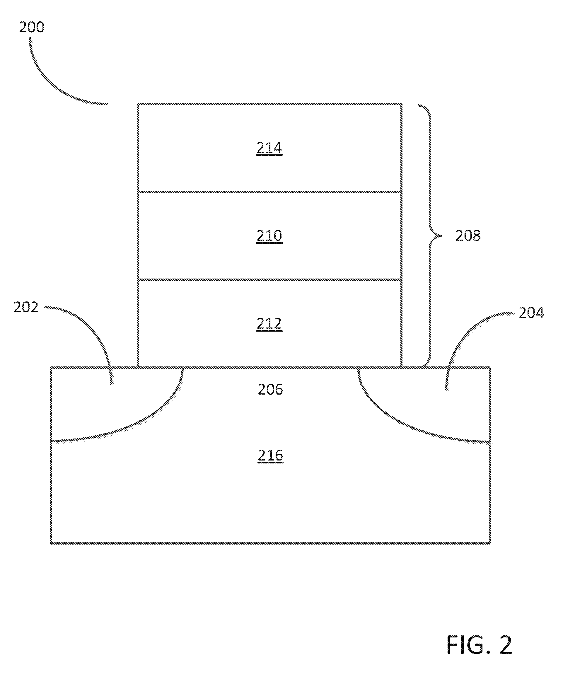
[0014] FIG. 2 illustrates a cross sectional schematic diagram of a device structure comprising a material film deposited according to the embodiments of the disclosure;
[0015] FIG. 3 illustrates a schematic diagram of a reaction system configured to perform the methods of the disclosure.
DETAILED DESCRIPTION OF EXEMPLARY EMBODIMENTS
[0016] Although certain embodiments and examples are disclosed below, it will be understood by those in the art that the invention extends beyond the specifically disclosed embodiments and/or uses of the invention and obvious modifications and equivalents thereof. Thus, it is intended that the scope of the invention disclosed should not be limited by the particular disclosed embodiments described below.
[0017] The illustrations presented herein are not meant to be actual views of any particular material, structure, or device, but are merely idealized representations that are used to describe embodiments of the disclosure.
[0018] As used herein, the term "cyclic deposition" may refer to the sequential introduction of precursors (reactants) into a reaction chamber to deposit a film over a substrate and includes deposition techniques such as atomic layer deposition and cyclical chemical vapor deposition.
[0019] As used herein, the term "cyclical chemical vapor deposition" may refer to any process wherein a substrate is sequentially exposed to two or more volatile precursors, which react and/or decompose on a substrate to produce a desired deposition.
[0020] As used herein, the term "substrate" may refer to any underlying material or materials that may be used, or upon which, a device, a circuit, or a film may be formed.
[0021] As used herein, the term "atomic layer deposition" (ALD) may refer to a vapor deposition process in which deposition cycles, preferably a plurality of consecutive deposition cycles, are conducted in a reaction chamber. Typically, during each cycle the precursor is chemisorbed to a deposition surface (e.g., a substrate surface or a previously deposited underlying surface such as material from a previous ALD cycle), forming a monolayer or sub-monolayer that does not readily react with additional precursor (i.e., a self-limiting reaction). Thereafter, if necessary, a reactant (e.g., another precursor or reaction gas) may subsequently be introduced into the process chamber for use in converting the chemisorbed precursor to the desired material on the deposition surface. Typically, this reactant is capable of further reaction with the precursor. Further, purging steps may also be utilized during each cycle to remove excess precursor from the process chamber and/or remove excess reactant and/or reaction byproducts from the process chamber after conversion of the chemisorbed precursor. Further, the term "atomic layer deposition," as used herein, is also meant to include processes designated by related terms such as, "chemical vapor atomic layer deposition", "atomic layer epitaxy" (ALE), molecular beam epitaxy (MBE), gas source MBE, or organometallic MBE, and chemical beam epitaxy when performed with alternating pulses of precursor composition(s), reactive gas, and purge (e.g., inert carrier) gas.
[0022] As used herein, the term "film" and "thin film" may refer to any continuous or non-continuous structures and material deposited by the methods disclosed herein. For example, "film" and "thin film" could include 2D materials, nanorods, nanotubes, or nanoparticles or even partial or full molecular layers or partial or full atomic layers or clusters of atoms and/or molecules. "Film" and "thin film" may comprise material or a layer with pinholes, but still be at least partially continuous.
[0023] As used herein, the term "work function metal" may refer to any conductive metal-containing material that results in an appropriate effective work function when formed in, on or over the gate dielectric of a semiconductor device.
[0024] As used herein, the term "metalorganic" or "organometallic" are used interchangeably and may refer to organic compounds containing a metal species.
[0025] Organometallic compounds may be considered to be subclass of metalorganic compounds having direct metal-carbon bonds.
[0026] A number of example materials are given throughout the embodiments of the current disclosure, it should be noted that the chemical formulas given for each of the example materials should not be construed as limiting and that the non-limiting example materials given should not be limited by a given example stoichiometry.
[0027] The present disclosure includes methods and device structures that may be used to form transistor gate structures comprising one or more work function metals, wherein the work function metals may be formed utilizing cyclical deposition processes, such as, for example, atomic layer deposition processes. The existing work function metals that may be utilized in the ALD formation of gate electrodes may have limitations due to their unsuitable effective work function values. For example, it is known that the effective work function of a material may vary as a function of its thickness. Therefore, as device geometries decrease in advance technology node applications, the thickness of the corresponding device films, such as the work function metal(s) of the gate electrode, may also decrease with an associated change in the value of effective work function. Such a change in the effective work function of the gate electrode may result in a non-ideal effective work function for both NMOS and PMOS device structures. Methods and structures are therefore required to provide a more desirable gate electrode. Examples of such methods and structures are disclosed in further detail herein.
[0028] In addition, the present disclosure also includes methods for depositing a conformal, uniform material film over a substrate, and particularly over a device structure including high aspect ratio features. For example, in a cyclical deposition process, it may be necessary to increase the dose of one of more of the vapor phase reactants involved in the deposition process to ensure that sufficient reactant contacts the entirety of the surface of the substrate. Attempts to increase the dosage of the vapor phase reactants in a cyclical deposition process may involve either increasing the pulse time or simply repeated pulsing multiple times. However, one problem with increasing the pulse time in vapor deposition apparatus, such as ALD or CVD reactors, is that a mere increase in the pulse time does not compensate for the increased surface area of the substrate, as the precursor concentration typically drops quickly with increased or longer pulse times. A mere increase in pulse time typically results in diminished concentration of the vapor phase reactant. Similarly, simply pulsing the same source chemical multiple times consecutively also leads to diminished precursor concentration in each subsequent pulse. Accordingly, the embodiments of the disclosure may include methods that utilize a micro pulsing process comprising two or more sequential micro pulses of vapor phase reactant and a micro purge of the substrate. In the micro pulsing process, the concentration of the vapor phase reactant provided into the reaction chamber, and contacting the substrate, may be substantially constant from pulse to pulse thereby supplying a uniform concentration of a vapor phase reactant to the substrate and allowing conformal, uniform deposition of material films. The micro pulsing process of the current disclosure may therefore provide a uniform, high dose of vapor phase reactant pulses to a reaction chamber, and the substrate within.
[0029] Therefore, the embodiments of the disclosure may comprise methods for depositing a material film on a substrate within a reaction chamber by a cyclical deposition process. In some embodiments, the methods may comprise: contacting the substrate with a first vapor phase reactant and purging the reaction chamber with a first main purge. The methods of the disclosure may also comprise: contacting the substrate with a second vapor phase reactant by two or more micro pulsing processes, wherein each micro pulsing process comprises: contacting the substrate with a micro pulse of a second vapor phase reactant; and purging the reaction chamber with a micro purge; wherein each of the micro pulses of the second vapor phase reactant provides a substantially constant concentration of the second vapor phase reactant into the reaction chamber. In some embodiments, the methods of the disclosure may also comprise, purging the reaction chamber with a second main purge.
[0030] A non-limiting example embodiment of a cyclical deposition process may include atomic layer deposition (ALD), wherein ALD is based on typically self-limiting reactions, whereby sequential and alternating pulses of reactants are used to deposit about one atomic (or molecular) monolayer of material per deposition cycle. The deposition conditions and precursors are typically selected to provide self-saturating reactions, such that an absorbed layer of one reactant leaves a surface termination that is non-reactive with the gas phase reactants of the same reactants. The substrate is subsequently contacted with a different reactant that reacts with the previous termination to enable continued deposition. Thus, each cycle of alternated pulses typically leaves no more than about one monolayer of the desired material. However, as mentioned above, the skilled artisan will recognize that in one or more ALD cycles more than one monolayer of material may be deposited, for example, if some gas phase reactions occur despite the alternating nature of the process.
[0031] In an ALD-type process for depositing a material film, such as, for example, a transition metal aluminum carbide film, one deposition cycle may comprise exposing the substrate to a first reactant, removing any unreacted first reactant and reaction byproducts from the reaction chamber, and exposing the substrate to a second reactant via two or more micro pulsing processes, followed by a second removal step. In some embodiments of the disclosure, the first reactant may comprise a metal vapor phase reactant ("the metal precursor") and the second reactant may comprise a carbon vapor phase reactant ("the carbon precursor").
[0032] Precursors may be separated by inert gases, such as argon (Ar) or nitrogen (N2), to prevent gas-phase reactions between reactants and enable self-saturating surface reactions. In some embodiments, however, the substrate may be moved to separately contact a first vapor phase reactant and a second vapor phase reactant. Because the reactions self-saturate, strict temperature control of the substrates and precise dosage control of the precursors may not be required. However, the substrate temperature is preferably such that an incident gas species does not condense into monolayers nor decompose on the surface. Surplus chemicals and reaction byproducts, if any, are removed from the substrate surface, such as by purging the reaction space or by moving the substrate, before the substrate is contacted with the next reactive chemical. Undesired gaseous molecules can be effectively expelled from a reaction space with the help of an inert purging gas. A vacuum pump may be used to assist in the purging.
[0033] Reactors capable of being used to deposit material films, such as, for example, transition metal aluminum carbides, can be used for the deposition processes described herein. Such reactors include ALD reactors, as well as CVD reactors, configured to provide the precursors. According to some embodiments, a showerhead reactor may be used. According to some embodiments, cross-flow, batch, minibatch, or spatial ALD reactors may be used.
[0034] The deposition processes described herein may optionally be carried out in a reactor or reaction chamber connected to a cluster tool. In a cluster tool, because each reaction chamber is dedicated to one type of process, the temperature of the reaction chamber in each module can be kept constant, which improves the throughput compared to a reactor in which the substrate is heated up to the process temperature before each run. Additionally, in a cluster tool it is possible to reduce the time to pump the reaction chamber to the desired process pressure levels between substrates. In some embodiments of the disclosure, the deposition process may be performed in a cluster tool comprising multiple reaction chambers, wherein each individual reaction chamber may be utilized to expose the substrate to an individual precursor gas and the substrate may be transferred between different reaction chambers for exposure to multiple precursors gases, the transfer of the substrate being performed under a controlled ambient to prevent oxidation/contamination of the substrate. In some embodiments of the disclosure, the deposition process may be performed in a cluster tool comprising multiple reaction chambers, wherein each individual reaction chamber may be configured to heat the substrate to a different deposition temperature.
[0035] A stand-alone reactor may be equipped with a load-lock. In that case, it is not necessary to cool down the reaction chamber between each run. In some embodiments, a deposition process for depositing a material film, such as a metal containing film, may comprise a plurality of deposition cycles, for example ALD cycles or cyclical CVD cycles.
[0036] In some embodiments, a cyclical deposition process may be used to form a material film on a substrate and the cyclical deposition process may be an ALD type process. In some embodiments, the cyclical deposition process may be a hybrid ALD/CVD or a cyclical CVD process. For example, in some embodiments, the growth rate of the ALD process may be low compared with a CVD process. One approach to increase the growth rate may be that of operating at a higher substrate temperature than that typically employed in an ALD process, resulting in a chemical vapor deposition process, but still taking advantage of the sequential introduction of precursors, such a process may be referred to as cyclical CVD.
[0037] According to some embodiments of the disclosure, ALD processes may be used to form a material film, such as, for example, a transition metal aluminum carbide, on a substrate, such as an integrated circuit work piece. In some embodiments, of the disclosure, each ALD cycle may comprise two distinct deposition steps or phases. In a first phase of the deposition cycle ("the metal phase"), the substrate surface on which deposition is desired may be contacted with a first vapor phase reactant comprising a metal precursor which chemisorbs on to the surface of the substrate, forming no more than about one monolayer of reactant species on the surface of the substrate. In a second phase of the deposition ("the carbon phase"), the substrate surface on which deposition is desired may be contacted with two or more micro pulses of a second vapor phase reactant comprising at least a carbon containing vapor phase reactant, i.e., the carbon precursor, wherein the material film may be deposited due to the reaction between the metal vapor phase reactant and the carbon vapor phase reactant.
[0038] In some embodiments of disclosure, a cyclical deposition process may be utilized to deposit a material film, such as, for example, a transition metal aluminum carbide film, and a non-limiting example of such a cyclical deposition process may be understood with reference to FIGS. 1A and 1B, wherein FIG. 1A illustrates the overall exemplary cyclical deposition process and FIG. 1B illustrates a sub-process of the overall process, the sub-process comprising a micropulsing process for providing a second vapor phase reactant to the substrate.
[0039] In more detail, FIG. 1A illustrates an exemplary overall cyclical deposition process 100 including a process block 110, which comprises, providing a substrate into a reaction chamber and heating the substrate to a desired deposition temperature. The reaction chamber utilized for the deposition may be an atomic layer deposition reaction chamber, or a chemical vapor deposition reaction chamber, or any of the reaction chambers as previously described herein. In some embodiments of the disclosure, the substrate may be heated to a desired deposition temperature during the cyclical deposition process. For example, the substrate may be heated to a substrate temperature of less than approximately 750.degree. C., or less than approximately 650.degree. C., or less than approximately 550.degree. C., or less than approximately 450.degree. C., or less than approximately 350.degree. C., or less than approximately 250.degree. C., or even less than approximately 150.degree. C. In some embodiments of the disclosure, the substrate temperature during the cyclical deposition process may be between 300.degree. C. and 750.degree. C., or between 400.degree. C. and 600.degree. C., or between 400.degree. C. and 450.degree. C.
[0040] Upon heating the substrate to a desired deposition temperature, the exemplary cyclical deposition process 100 may continue with a process block 120, which comprises contacting the substrate with a first vapor phase reactant and particularly, in some embodiments, contacting the substrate with a first vapor phase reactant comprising one or more metal vapor phase reactants, i.e., the metal precursor. In some embodiments of the disclosure, the one or more metal vapor phase reactants may comprise a transition metal component. For example, the transition metal precursor may comprise at least one of the transition metals selected from the group consisting of, titanium (Ti), zirconium (Zr), hafnium (Hf), vanadium (V), niobium (Nb), tantalum (Ta), chromium (Cr), molybdenum (Mo), and tungsten (W).
[0041] In some embodiments of the disclosure, the metal vapor phase reactant may comprise a metal halide, such as, for example, one or more of a metal chloride, a metal iodide, a metal fluoride, or a metal bromide. In some embodiments, the metal vapor phase reactant may comprise a transition metal halide, such as, for example, one or more of a transition metal chloride, a transition metal iodide, a transition metal fluoride, or a transition metal bromide. As a non-limiting example embodiment, the first metal vapor phase reactant may comprise a titanium halide, such as, for example, titanium tetrachloride (TiCl.sub.4).
[0042] In some embodiments of the disclosure, contacting the substrate with a first vapor phase reactant comprising a metal precursor may comprise exposing the substrate to the metal precursor for a time period of between about 0.01 seconds and about 60 seconds, between about 0.05 seconds and about 10 seconds, or between about 0.1 seconds and about 5.0 seconds. In addition, during the pulsing of the metal containing precursor, the flow rate of the metal precursor may be less than 2000 sccm, or less than 500 sccm, or even less than 100 sccm. In addition, during the pulsing of the metal precursor over the substrate the flow rate of the metal precursor may range from about 1 to 2000 sccm, from about 5 to 1000 sccm, or from about 10 to about 500 sccm.
[0043] The exemplary cyclic deposition process 100 of FIG. 1A may continue with a process block 130 comprising, purging the reaction chamber with a first main purge. For example, excess first vapor phase reactant and reaction byproducts (if any) may be removed from the surface of the substrate, e.g., by pumping with an inert gas. In some embodiments of the disclosure, the first main purge process may comprise a purge cycle wherein the substrate surface is purged for a time period of less than approximately 5.0 seconds, or less than approximately 3.0 seconds, or even less than approximately 2.0 seconds. Excess first vapor phase reactant, such as, for example, excess metal precursors and any possible reaction byproducts may be removed with the aid of a vacuum, generated by a pumping system in fluid communication with the reaction chamber.
[0044] Upon purging the reaction chamber with the first main purge, i.e., the process block 130 of FIG. 1A, the exemplary cyclical deposition process 100 may continue with a process block 140 comprising, contacting the substrate with a second vapor phase reactant and particularly, in some embodiments of the disclosure, contacting the substrate with a carbon precursor by two or more micro pulsing processes.
[0045] In more detail, FIG. 1B illustrates the process block 140 as the sub-process 140' and details the particular embodiments of the micro pulsing process for contacting the substrate with two or more micro pulses of the second vapor phase reactant, i.e., the carbon precursor. The sub-process 140' may proceed with process block 142 comprising, contacting the substrate with a micro pulse of the second vapor phase reactant and in particular, in certain embodiments of the disclosure, contacting the substrate with a micro pulse of a carbon precursor.
[0046] In some embodiments of the disclosure, the second vapor phase reactant may comprise one or more carbon vapor phase reactants, i.e., the carbon precursor. In some embodiments, the one or more carbon vapor phase reactants may comprise one or more metalorganic precursors and the metal component of the metalorganic precursor may also be incorporated into the material film as it is deposited. In some embodiments of the disclosure, the one or more carbon precursors may comprise at least one metalorganic precursor, wherein the metalorganic precursors comprises an aluminum (Al) component, i.e., the aluminum metalorganic precursor. For example, the aluminum metalorganic precursor may comprise at least one of trimethylaluminum (TMA), triethylaluminum (TEA), dimethylaluminumhydride (DMAH), or tritertbutylaluminum (TTBA). As a non-limiting example, the first vapor phase reactant may comprise titanium tetrachloride (TiCl4) and the second vapor phase reactant may comprise triethylaluminum (TEA), and the material film deposited by the exemplary cyclical deposition process may comprise a titanium aluminum carbide (TiAlC), wherein the TiCl4 provides the titanium (Ti) to the material film and the TEA provides both the aluminum (Al) and carbon (C) to the material film.
[0047] In some embodiments of the disclosure, the second vapor phase reactant may be supplied to the reaction chamber from a source vessel, i.e., a source vessel containing the second reactant. In some embodiments, the source vessel may contain the second reactant as a solid source, a liquid source, or a gaseous source. In some embodiments, the second reactant may comprise a solid dissolved in a suitable solvent in order to provide a liquid source of the second reactant. In some embodiments of the disclosure, the source vessel and any intervening gas delivery lines between the source vessel and the reaction chamber may be heated to a desired temperature to increase the vapor pressure of the reactant and prevent adsorption and condensation of the precursor, therefore enabling a satisfactory flow of the vapor phase reactant from the source vessel to the reaction chamber. In some embodiments of the disclosure, the second vapor phase reactant, e.g., the carbon precursor, may comprise a low vapor pressure reactant. For example, the second reactant may comprise a low vapor pressure reactant which has a vapor pressure of less than 1 Torr at room temperature, or less than 0.1 Torr at room temperature, or even less than 0.01 Torr at room temperature.
[0048] In some embodiments of the disclosure, contacting the substrate with a micro pulse of the second vapor phase reactant, e.g., a carbon precursor, may comprise micro pulsing, i.e., contacting, the substrate to the carbon precursor for a time period of between about 0.01 seconds and about 60 seconds, between about 0.05 seconds and about 10 seconds, or between about 0.1 seconds and about 5.0 seconds. In some embodiment of the disclosure, contacting the substrate with a micro pulse of the second vapor phase reactant, e.g., a carbon precursor, may comprise micro pulsing, i.e., contacting, the substrate to the carbon precursor for a time period of less than approximately 2 seconds, or less than approximately 1 second, or less than approximately 0.5 seconds, or even less than approximately 0.1 seconds.
[0049] Upon contacting the substrate with a micro pulse of the second vapor phase reactant, the sub-process 140' of FIG. 1B may proceed with a process block 144 comprising, purging the reaction chamber with a micro purge. For example, excess second vapor phase reactant and reaction byproducts (if any) may be removed from the surface of the substrate, e.g., by pumping with an inert gas. In some embodiments of the disclosure, the purge process may comprise a micro purge wherein the substrate surface is purged for a time period of between approximately 0.1 seconds and approximately 10 seconds, or between approximately 0.5 seconds and approximately 3 seconds, or even between approximately 1 second and 2 seconds. In some embodiments of the disclosure, the micro purging process may purge the surface of the substrate for a time period of less than 1 second, or less than 0.5 seconds, or less than 0.2 seconds, or even less than 0.1 seconds. Excess second vapor phase reactant, such as, for example, excess carbon precursor and any possible reaction byproducts may be removed with the aid of a vacuum, generated by a pumping system in fluid communication with the reaction chamber.
[0050] During the micro purging process, i.e., simultaneously to performing the micro purging process of the process block 144, the sub-process 140' may also comprise, replenishing the concentration of the second vapor source at the source vessel. In more detail, as the sub-process 140' contacts the substrate with a micro pulse of the second vapor phase precursors, a certain concentration of the second vapor phase precursor may be depleted from the source vessel and/or the gas delivery lines disposed between the source vessel and the reaction chamber. If repeated micro pulses of the second vapor phase precursor are supplied to the reaction chamber without an intervening micro purging process, then the precursor concentration entering the reaction chamber (and subsequently contacting the substrate within the reaction chamber) may decrease over time and the decrease in concentration of the precursor in each micro pulse may result in unsatisfactory deposition characteristics, such as, for example, non-uniform thickness of the deposited material film.
[0051] Upon purging the reaction chamber with a micro purge, i.e., the process block 144, the micro pulsing process may be repeated at least once, or may be repeated multiple times. For example, the sub-process 140' may comprise a sub-cycle including, contacting the substrate with a micro pulse of a second vapor phase reactant (process block 142), and purging the reaction chamber with a micro purge (process block 144), wherein the sub-cycle may be repeated at least once, or may be repeated multiple times. In particular embodiments of the disclosure, having repeated the micro pulsing process at least once, the sub-process 140' may continue with a decision gate 146 which determines if the sub-process 140' is continued for a further sub-cycle or if the sub-process 140' exits at a process block 148 and returns to the cyclical deposition process 100 of FIG. 1A. The decision gate 146 may be determined based upon the desired dose of the second vapor phase reactant to be provided to the reaction chamber and particular provided to a substrate within the reaction chamber. In some embodiments of the disclosure, the sub-cycle of sub-process 140' may be repeated two (2) or more times, three (3) of more times, five (5) or more times, or even ten (10) or more times. As the number of sub-cycles of sub-process 140' is increased, the dose of the second vapor phase reactant provided to the reaction chamber may accordingly increase until a desired dose of the second vapor phase reactant is provided into the reaction chamber.
[0052] In some embodiments of the disclosure, each sub-cycle, of sub-process 140', comprises contacting the substrate with a micro pulse of the second vapor phase reactant, wherein each of the micro pulses of the second vapor phase reactant provides a substantially constant concentration of the second vapor phase reactant into the reaction chamber. Therefore, as opposed to known cyclical deposition methods, the methods of the current disclosure may provide multiple micro pulses of a vapor phase reactant to a reaction chamber without a decrease in the concentration of the vapor phase reactant between each individual micro pulses. Each micro pulse provides a substantially constant concentration of vapor phase reactant to the reaction chamber and as the number of micro pulses increases the desired dose of reactant contacting the substrate may be increased until a desired dose is reached and the sub-process 140' exits back into the cyclical deposition process 100 of FIG. 1A.
[0053] After completing the sub-process 140', the exemplary cyclical deposition cycle 100 may continue with a process block 150 (FIG. 1A) which comprises, purging the reaction chamber with a second main purge. For example, excess second vapor phase reactant and reaction byproducts (if any) may be removed from the surface of the substrate, e.g., by pumping with an inert gas. In some embodiments of the disclosure, the second main purge process may comprise a purge cycle wherein the substrate surface is purged for a time period of less than approximately 5.0 seconds, or less than approximately 3.0 seconds, or even less than approximately 2.0 seconds. Excess second vapor phase reactant, such as, for example, excess carbon precursor(s) and any possible reaction byproducts may be removed with the aid of a vacuum, generated by a pumping system in fluid communication with the reaction chamber.
[0054] Upon completion of the second main purge process, i.e., process block 150, the exemplary cyclical deposition process 100 may continue with a decision gate 160, wherein the decision gate 160 is dependent on the thickness of the material film deposited. For example, if the material film is deposited at an insufficient thickness for the desired device application, the cyclical deposition process may be repeated by returning to the process block 120 and continuing through a further deposition cycle, wherein one deposition cycle comprises, contacting the substrate with a metal precursor (process block 120), purging the reaction chamber with a first main purge (process block 130), contacting the substrate with a carbon precursor by two or more micro pulsing processes (process block 140), and purging the reaction chamber with a second main purge (process block 150). A deposition cycle, of cyclical deposition process 100, may be repeated one or more times until a desired thickness of the material film is deposited over the substrate, upon which the cyclical deposition process 100 may exit at a process block 170 and the substrate may be subjected to further fabrication processes to complete the device structures.
[0055] It should be appreciated that in some embodiments of the disclosure, the order of contacting of the substrate with the first vapor phase reactant and the second vapor phase reactant may be such that the substrate is first contacted with the second vapor phase reactant followed by the first vapor phase reactant. In addition, in some embodiments, the cyclical deposition process may comprise, contacting the substrate with the first vapor phase reactant one or more times prior to contacting the substrate with the second vapor phase reactant two or more times. In addition, in some embodiments of the disclosure, the micro pulsing process may be utilized for contacting the substrate with the first vapor phase reactant, in addition to, or as an alternative to micro pulsing the second vapor phase reactant.
[0056] In addition, some embodiments of the disclosure may comprise non-plasma reactants, e.g., the first and second vapor phase reactants may be substantially free of ionized reactive species. In some embodiments, the first and second vapor phase reactants are substantially free of ionized reactive species, excited species, or radical species. For example, both the first vapor phase reactant and the second vapor phase reactant may comprise non-plasma reactants to prevent ionization damage of the underlying substrate and the associated defect thereby created.
[0057] In some embodiments of the disclosure, the growth rate of the material film, e.g., a transition metal aluminum carbide, may be from about 0.005 .ANG./cycle to about 5 .ANG./cycle, from about 0.01 .ANG./cycle to about 2.0 .ANG./cycle. In some embodiments, the growth rate of the material film may be from about 0.1 .ANG./cycle to about 10 .ANG./cycle. In some embodiments the growth rate of the material film is more than about 0.05 .ANG./cycle, more than about 0.1 .ANG./cycle, more than about 0.15 .ANG./cycle, more than about 0.20 .ANG./cycle, more than about 0.25 .ANG./cycle or more than about 0.3 .ANG./cycle. In some embodiments the growth rate of the material film is less than about 2.0 .ANG./cycle, less than about 1.0 .ANG./cycle, less than about 0.75 .ANG./cycle, less than about 0.5 .ANG./cycle, or less than about 0.2 .ANG./cycle. In some embodiments of the disclosure, the material film comprises a transition metal aluminium carbide deposited with a growth rate of approximately 5 .ANG./cycle.
[0058] Material films deposited by the cyclical deposition processes disclosed herein, such as, for example, a transition metal aluminum carbide, may be continuous films. In some embodiments, the material film, e.g., a transition metal aluminum carbide, may be continuous at a thickness below approximately 100 nanometers, or below approximately 60 nanometers, or below approximately 50 nanometers, or below approximately 40 nanometers, or below approximately 30 nanometers, or below approximately 20 nanometers, or below approximately 10 nanometers, or even below approximately 5 nanometers. The continuity referred to herein can be physical continuity or electrical continuity. In some embodiments of the disclosure the thickness at which a material film may be physically continuous may not be the same as the thickness at which a film is electrically continuous, and vice versa.
[0059] In some embodiments of the disclosure, the material film deposited according to the cyclical deposition processes described herein, e.g., a transition metal aluminum carbide, may have a thickness from about 20 nanometers to about 100 nanometers, or about 20 nanometers to about 60 nanometers. In some embodiments, a material film deposited according to some of the embodiments described herein may have a thickness greater than about 20 nanometers, or greater than about 30 nanometers, or greater than about 40 nanometers, or greater than about 50 nanometers, or greater than about 60 nanometers, or greater than about 100 nanometers, or greater than about 250 nanometers, or greater than about 500 nanometers, or greater. In some embodiments a material film, e.g., a transition metal aluminum carbide, deposited according to some of the embodiments described herein may have a thickness of less than about 50 nanometers, or less than about 30 nanometers, or less than about 20 nanometers, or less than about 15 nanometers, or less than about 10 nanometers, or less than about 5 nanometers, or less than about 3 nanometers, or less than about 2 nanometers, or even less than about 1 nanometer.
[0060] The cyclical deposition methods described herein, i.e., utilizing two or micro pulsing processes, may enable the deposition of material films, e.g., transition metal aluminum carbide films, with reduced thickness non-uniformities. For example, the material may comprise a titanium aluminum carbide (TiAlC) film deposited with a thickness non-uniformity having a standard deviation of less than 2% one-sigma, or less than 1.5% one-sigma, or less than 1% one-sigma, or even less than 0.5% one-sigma. It should be noted that the thickness non-uniformities described herein may include a 3 millimeter edge exclusion.
[0061] In some embodiments of the disclosure, the material film may be deposited on a substrate comprising high aspect ratio features, e.g., a three-dimensional, non-planar substrate. In some embodiments, the step coverage of the material film, e.g., a transition metal aluminum carbide, may be equal to or greater than about 50%, or greater than about 80%, or greater than about 90%, or greater than about 95%, or greater than about 98%, or about 99% or greater on structures having aspect ratios (height/width) of greater than 2, or greater than 5, or greater than 10, or greater than 25, or greater than 50, or even greater than 100.
[0062] In some embodiments of the disclosure the first vapor phase reactant may comprise a transition metal reactant and the second vapor phase reactant may comprise a metalorganic reactant, such as, for example, an aluminum containing metalorganic reactant. In such embodiments, the material film deposited may comprise a transition metal carbide and in particular embodiments the material film deposited may comprise, a transition metal aluminum carbide. For example, a transition metal aluminum carbide may be represented by the general formula XAlC, wherein X comprises a transition metal, Al is aluminum, and C is carbon. In some embodiments, the transition metal aluminum carbide may comprise a transition metal selected from the group consisting of, titanium (Ti), zirconium (Zr), hafnium (Hf), vanadium (V), niobium (Nb), tantalum (Ta), chromium (Cr), molybdenum (Mo), and tungsten (W). In some embodiments of the disclosure, the transition metal may comprise titanium and the transition metal aluminum carbide may comprise titanium aluminum carbide (TiAlC).
[0063] In some embodiments of the disclosure, the material film deposited comprises a transition metal aluminum carbide (XAlC), wherein the transition metal aluminum carbide (XAlC) contains an aluminum content of greater than 10 atomic %, or greater than 20 atomic %, or greater than 30 atomic %, or greater than 40 atomic %, or even greater than 50 atomic %. In some embodiments of the disclosure, the material film deposited comprises a titanium aluminum carbide (TiAlC) film which contains an aluminum content of greater than 20 atomic-%, or greater than 30 atomic %, or greater than 35 atomic %, or even greater than 40 atomic %. In embodiments wherein the material film comprises a titanium aluminum carbide (TiAlC) film, the TiAlC film may contain a titanium content of less than 40 atomic %, or less than 20 atomic %, or even less than 10 atomic %. In addition, in embodiments wherein the material film comprises a titanium aluminum carbide (TiAlC) film, the TiAlC film may contain a carbon content of greater than 20 atomic %, or greater than 30 atomic %, or even greater than 40 atomic %. In some embodiments of the disclosure the material film may comprise a titanium aluminum carbide (TiAlC) film which may comprise an average titanium (Ti) to aluminum content (Ti:Al) of less than 0.3, or less than 0.2, or less than 0.15, or even less than 0.10. In the embodiments outlined herein, the atomic concentration of an element may be determined utilizing Rutherford backscattering (RB S).
[0064] In additional embodiments, the material film may comprise a transition metal aluminum carbide, e.g., a titanium aluminum (TiAlC) film, which may comprise less than about 20 atomic % oxygen, or less than about 10 atomic % oxygen, or less than about 5 atomic % oxygen, or even less than about 2 atomic % oxygen. In further embodiments, the transition metal aluminum carbide film may comprise, less than about 10 atomic % hydrogen, or less than about 5 atomic % of hydrogen, or less than about 2 atomic % of hydrogen, or even less than about 1 atomic % of hydrogen.
[0065] The material films, e.g., transition metal aluminum carbide films, deposited by the cyclical deposition processes disclosed herein may be utilized in a variety of applications. As a non-limiting example embodiment, the material film may comprise a transition metal aluminum carbide film utilized as a work function metal in a semiconductor transistor application, such as a planar transistor structure or a multiple gate transistor (e.g., FinFET). In more detail, and with reference to FIG. 2, a semiconductor device structure 200 may comprise a semiconductor body 216 and a gate electrode 210 comprising a transition metal aluminum carbide (e.g., TiAlC) disposed over the semiconductor body 216. In some embodiments, the semiconductor device structure 200 may comprise a transistor structure and may also include a source region 202, a drain region 204, and a channel region 206 disposed therebetween. A transistor gate structure 208 may comprise an electrode, i.e., a gate electrode, which may be separated from the channel region 206 by a gate dielectric 212. According to the present disclosure, the gate electrode 210 may comprise a transition metal aluminum carbide, such as, for example, a titanium aluminum carbide (TiAlC), deposited by the cyclical deposition methods described herein. As shown in FIG. 2, in some embodiments the transistor gate structure 208 may further comprise one or more additional conductive layers 214 formed on the gate electrode 210. The one or more additional conductive layers 214 may comprise at least one of a polysilicon, a refractory metal, a further transition metal carbide, and a transition metal nitride.
[0066] In some embodiments of the disclosure, the gate electrode 210 may comprise a titanium aluminum carbide (TiAlC) film and the transistor gate structure 208 may have an effective work function of less than approximately 4.5 eV, or less than approximately 4.3 eV, or even less than approximately 4.1 eV. In some embodiments, the gate electrode 210 may comprise a titanium aluminum carbide (TiAlC) film and the transistor gate structure 208 may have an effective work function less than approximately 4.3 eV, wherein the titanium aluminum carbide (TiAlC) film has a thickness of less than 6 nanometers, or less than 3 nanometers, or even less than 2 nanometers.
[0067] Embodiments of the disclosure may also include a reaction system configured for forming the material films, e.g., transition metal aluminum carbide films, of the present disclosure. In more detail, FIG. 3 schematically illustrates a reaction system 300 including a reaction chamber 302 that further includes mechanism for retaining a substrate (not shown) under predetermined pressure, temperature, and ambient conditions, and for selectively exposing the substrate to various gases. A precursor reactant source 304 may be coupled by conduits or other appropriate means 304A to the reaction chamber 302, and may further couple to a manifold, valve control system, mass flow control system, or mechanism to control a gaseous precursor originating from the precursor reactant source 304. A precursor (not shown) supplied by the precursor reactant source 304, the reactant (not shown), may be liquid or solid under room temperature and standard atmospheric pressure conditions. Such a precursor may be vaporized within a reactant source vacuum vessel, which may be maintained at or above a vaporizing temperature within a precursor source chamber. In such embodiments, the vaporized precursor may be transported with a carrier gas (e.g., an inactive or inert gas) and then fed into the reaction chamber 302 through conduit 304A. In other embodiments, the precursor may be a vapor under standard conditions. In such embodiments, the precursor does not need to be vaporized and may not require a carrier gas. For example, in one embodiment the precursor may be stored in a gas cylinder. The reaction system 300 may also include additional precursor reactant sources, such as precursor reactant source 306, which may also be coupled to the reaction chamber by conduits 306A as described above.
[0068] A purge gas source 308 may also be coupled to the reaction chamber 302 via conduits 308A, and selectively supplies various inert or noble gases to the reaction chamber 302 to assist with the removal of precursor gas or waste gases from the reaction chamber. The various inert or noble gases that may be supplied may originate from a solid, liquid or stored gaseous form.
[0069] The reaction system 300 of FIG. 3 may also comprise a system operation and control mechanism 310 that provides electronic circuitry and mechanical components to selectively operate valves, manifolds, pumps and other equipment included in the reaction system 300. Such circuitry and components operate to introduce precursors, purge gases from the respective precursor sources 304, 306 and purge gas source 308. The system operation and control mechanism 310 also controls timing of gas pulse sequences, temperature of the substrate and reaction chamber, and pressure of the reaction chamber and various other operations necessary to provide proper operation of the reaction system 300. The operation and control mechanism 310 can include control software and electrically or pneumatically controlled valves to control flow of precursors, reactants, and purge gases into and out of the reaction chamber 302. The control system can include modules such as a software or hardware component, e.g., a FPGA or ASIC, which performs certain tasks. A module can advantageously be configured to reside on the addressable storage medium of the control system and be configured to execute one or more processes.
[0070] Those of skill in the relevant arts appreciate that other configurations of the present reaction system are possible, including a different number and kind of precursor reactant sources and purge gas sources. Further, such persons will also appreciate that there are many arrangements of valves, conduits, precursor sources, purge gas sources that may be used to accomplish the goal of selectively feeding gases into reaction chamber 302. Further, as a schematic representation of a reaction system, many components have been omitted for simplicity of illustration, and such components may include, for example, various valves, manifolds, purifiers, heaters, containers, vents, and/or bypasses.
[0071] The example embodiments of the disclosure described above do not limit the scope of the invention, since these embodiments are merely examples of the embodiments of the invention, which is defined by the appended claims and their legal equivalents. Any equivalent embodiments are intended to be within the scope of this invention. Indeed, various modifications of the disclosure, in addition to those shown and described herein, such as alternative useful combination of the elements described, may become apparent to those skilled in the art from the description. Such modifications and embodiments are also intended to fall within the scope of the appended claims.
* * * * *
D00000
D00001
D00002
D00003
D00004
XML
uspto.report is an independent third-party trademark research tool that is not affiliated, endorsed, or sponsored by the United States Patent and Trademark Office (USPTO) or any other governmental organization. The information provided by uspto.report is based on publicly available data at the time of writing and is intended for informational purposes only.
While we strive to provide accurate and up-to-date information, we do not guarantee the accuracy, completeness, reliability, or suitability of the information displayed on this site. The use of this site is at your own risk. Any reliance you place on such information is therefore strictly at your own risk.
All official trademark data, including owner information, should be verified by visiting the official USPTO website at www.uspto.gov. This site is not intended to replace professional legal advice and should not be used as a substitute for consulting with a legal professional who is knowledgeable about trademark law.