Wafer Polishing Pad And Method Of Wafer Polishing Using The Same
Kim; Seok Ryul ; et al.
U.S. patent application number 16/052294 was filed with the patent office on 2019-06-27 for wafer polishing pad and method of wafer polishing using the same. The applicant listed for this patent is SAMSUNG ELECTRONICS CO., LTD.. Invention is credited to Seok Ryul Kim, Sunghyup Kim, Sanghoon Lee.
| Application Number | 20190193238 16/052294 |
| Document ID | / |
| Family ID | 66949235 |
| Filed Date | 2019-06-27 |


| United States Patent Application | 20190193238 |
| Kind Code | A1 |
| Kim; Seok Ryul ; et al. | June 27, 2019 |
WAFER POLISHING PAD AND METHOD OF WAFER POLISHING USING THE SAME
Abstract
A wafer polishing pad includes a first pad having a first surface configured to receive a platen. A protrusion is disposed on the first surface of the first pad. The protrusion is disposed on an edge region of the first pad in a plan view such that a side surface of the protrusion makes contact with a side surface of the platen when the first pad is disposed on the platen.
| Inventors: | Kim; Seok Ryul; (Hwaseong-si, KR) ; Kim; Sunghyup; (Hwaseong-si, KR) ; Lee; Sanghoon; (Seoul, KR) | ||||||||||
| Applicant: |
|
||||||||||
|---|---|---|---|---|---|---|---|---|---|---|---|
| Family ID: | 66949235 | ||||||||||
| Appl. No.: | 16/052294 | ||||||||||
| Filed: | August 1, 2018 |
| Current U.S. Class: | 1/1 |
| Current CPC Class: | B24B 37/26 20130101; B24B 37/22 20130101 |
| International Class: | B24B 37/26 20060101 B24B037/26; B24B 37/22 20060101 B24B037/22 |
Foreign Application Data
| Date | Code | Application Number |
|---|---|---|
| Dec 27, 2017 | KR | 10-2017-0180750 |
Claims
1. A wafer polishing pad, comprising: a first pad having a first surface configured to receive a platen; and a protrusion disposed on the first surface of the first pad, wherein the protrusion is disposed on an edge region of the first pad in a plan view such that a side surface of the protrusion makes contact with a side surface of the platen when the first pad is disposed on the platen.
2. The wafer polishing pad of claim 1, wherein the protrusion exposes a central region of the first surface of the first pad, and when viewed in the plan view, the protrusion circumscribes the central region of the first pad.
3. The wafer polishing pad of claim 1, wherein the protrusion comprises a vent groove disposed within a bottom surface of the protrusion.
4. The wafer polishing pad of claim 3, wherein a floor surface of the vent groove is located at substantially a same level as that of the first surface of the first pad.
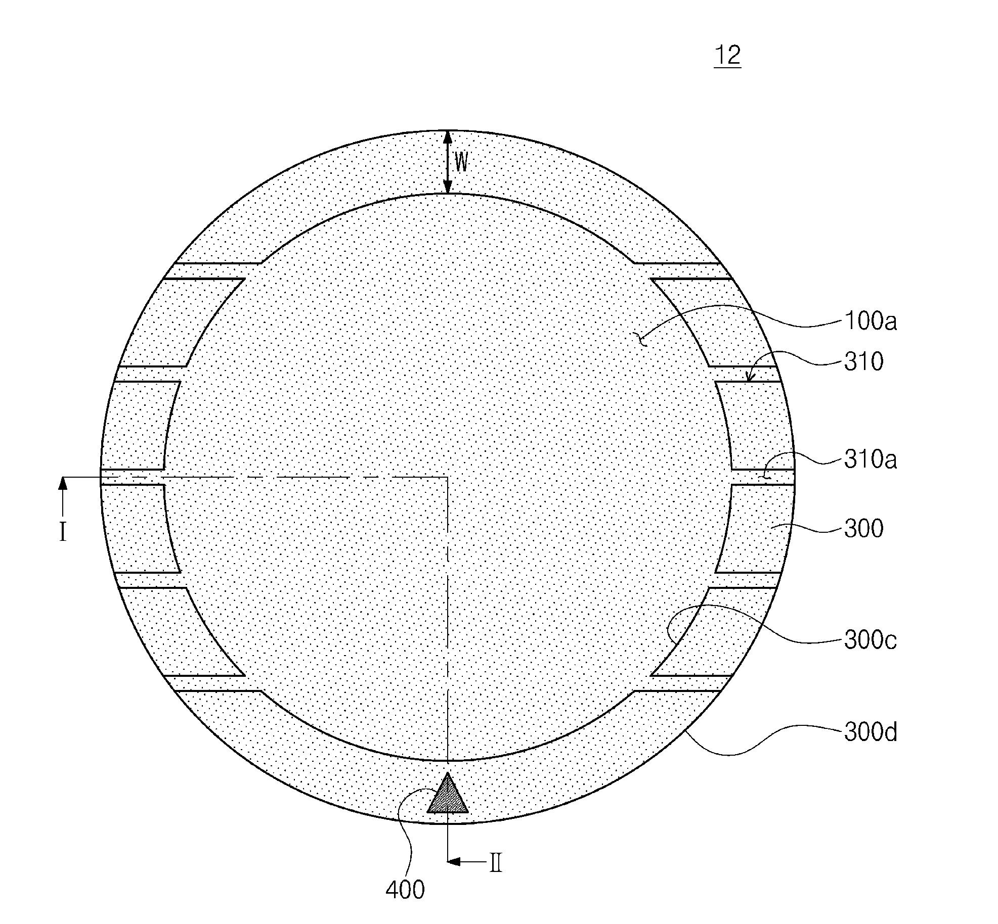
5. The wafer polishing pad of claim 3, further comprising a mark disposed on the bottom surface of the protrusion.
6. The wafer polishing pad of claim 3, further comprising an adhesive layer covering a portion of the first surface of the first pad, wherein the portion of the first surface of the first pad is exposed by the protrusion.
7. The wafer polishing pad of claim 1, wherein a groove is disposed on a second surface of the first pad, wherein the second surface of the first pad is opposite to the first surface.
8. The wafer polishing pad of claim 1, further comprising: a second pad disposed on the first pad; and an adhesive layer disposed between the first pad and the second pad.
9. The wafer polishing pad of claim 8, wherein a groove is disposed on a second surface of the second pad, wherein the second surface of the second pad faces away from the first pad.
10. The wafer polishing pad of claim 1, wherein a topmost portion of an edge region of a second surface of the first pad is located at substantially the same level as that of a topmost portion of a central region of the second surface of the first pad, wherein the second surface of the first pad is opposite to the first surface of the first pad.
11. A wafer polishing pad, comprising: a top surface including a groove; a first bottom surface opposite to the top surface and corresponding to a central region of the polishing pad; and a second bottom surface opposite to the top surface and corresponding to an edge region of the polishing pad, wherein the second bottom surface is located at a lower level than that of the first bottom surface.
12. The wafer polishing pad of claim 11, wherein the second bottom surface has a closed loop shape.
13. The wafer polishing pad of claim 11, further comprising a vent groove disposed within the second bottom surface, wherein a floor surface of the vent groove is connected to the first bottom surface.
14. The wafer polishing pad of claim 13, further comprising an adhesive layer disposed on the first bottom surface.
15-20. (canceled)
21. A wafer polishing pad, comprising: a polishing surface configured to mechanically polish a wafer; a receiving surface, opposite to the polishing surface, configured to make contact with a top surface of a platen; and a ring disposed on the receiving surface and configured to make contact with a side surface of the platen.
22. The wafer polishing pad of claim 21, wherein the ring of the polishing wafer is configured to buttress a portion of the polishing surface that extends beyond the platen.
23. The wafer polishing pad of claim 21, wherein the wafer polishing pad comprises a first pad and a second pad that are joined together by an adhesive layer, the first pad including the polishing surface and the second pad including the receiving surface.
Description
CROSS-REFERENCE TO RELATED APPLICATIONS
[0001] This U.S. nonprovisional application claims priority under 35 U.S.C .sctn. 119 to Korean Patent Application No. 10-2017-0180750 filed on Dec. 27, 2017, in the Korean Intellectual Property Office, the entire contents of which are hereby incorporated by reference.
TECHNICAL FIELD
[0002] The present disclosure relate to a polishing pad, and more particularly, to a wafer polishing pad and a method of wafer processing using the wafer polishing pad.
DISCUSSION OF THE RELATED ART
[0003] An integrated circuit is generally formed by successively disposing conductors, semiconductors, and/or insulators on a wafer. After each layer is disposed, the layer is etched to define the circuit. As layers are successively disposed and etched, the wafer gradually becomes rough on its exposed surface. To correct for this roughness, the wafer may be periodically planarized to flatten the exposed surface of the wafer. A chemical mechanical polishing process may be employed in planarizing the wafer. The chemical mechanical polishing process may use a polishing pad to polish the wafer.
SUMMARY
[0004] A wafer polishing pad includes a first pad having a first surface configured to receive a platen. A protrusion is disposed on the first surface of the first pad. The protrusion is disposed on an edge region of the first pad in a plan view such that a side surface of the protrusion makes contact with a side surface of the platen when the first pad is disposed on the platen.
[0005] A wafer polishing pad includes a top surface including a groove. A first bottom surface opposite to the top surface corresponds to a central region of the polishing pad. A second bottom surface opposite to the top surface corresponds to an edge region of the polishing pad. The second bottom surface is located at a lower level than that of the first bottom surface.
[0006] A wafer polishing method includes preparing a polishing pad comprising a first pad and a protrusion. The protrusion is disposed on an edge region of a first surface of the first pad. The polishing pad is placed on a platen such that the first surface of the first pad faces the platen. A wafer is polished using the polishing pad. Placing the polishing pad on the platen includes causing the protrusion of the polishing pad to make contact with a sidewall of the platen.
[0007] A wafer polishing pad includes a polishing surface configured to mechanically polish a wafer. A receiving surface, opposite to the polishing surface, is configured to make contact with a top surface of a platen. A ring is disposed on the receiving surface and the ring is configured to make contact with a side surface of the platen.
BRIEF DESCRIPTION OF THE DRAWINGS
[0008] A more complete appreciation of the present disclosure and many of the attendant aspects thereof will be readily obtained as the same becomes better understood by reference to the following detailed description when considered in connection with the accompanying drawings, wherein:
[0009] FIG. 1A is a plan view illustrating a polishing pad according to exemplary embodiments of the present disclosure;
[0010] FIG. 1B is a plan view illustrating grooves of a polishing pad according to exemplary embodiments of the present disclosure;
[0011] FIG. 1C is a cross-sectional view taken along line I-II of FIG. 1A;
[0012] FIG. 2 is a cross-sectional view illustrating a polishing pad according to exemplary embodiments of the present disclosure;
[0013] FIG. 3A is a plan view illustrating a polishing pad according to exemplary embodiments of the present disclosure;
[0014] FIG. 3B is a cross-sectional view taken along line I-II of FIG. 3A;
[0015] FIG. 3C is a cross-sectional view illustrating an adhesive layer attaching method according to exemplary embodiments of the present disclosure;
[0016] FIG. 4 is a flow chart illustrating a wafer polishing method according to exemplary embodiments of the present disclosure;
[0017] FIG. 5 is a perspective view illustrating a wafer polishing method according to exemplary embodiments of the present disclosure; and
[0018] FIG. 6 is a cross-sectional view illustrating a polishing pad associated with a platen in accordance with exemplary embodiments of the present disclosure.
DETAILED DESCRIPTION OF EMBODIMENTS
[0019] In describing exemplary embodiments of the present disclosure illustrated in the drawings, specific terminology is employed for sake of clarity. However, the present disclosure is not intended to be limited to the specific terminology so selected, and it is to be understood that each specific element includes all technical equivalents which operate in a similar manner. In the specification and the various figures, like reference numerals may indicate like components.
[0020] Exemplary embodiments of the present invention may utilize a wafer polishing pad and a wafer polishing method using the same.
[0021] FIG. 1A is a plan view illustrating a polishing pad according to exemplary embodiments of the present disclosure. FIG. 1B is a plan view illustrating grooves disposed on a polishing pad, according to exemplary embodiments of the present disclosure, showing a top surface of the polishing pad. FIG. 1C is a cross-sectional view taken along line I-II of FIG. 1A.
[0022] Referring to FIGS. 1A to 1C, a polishing pad 10 may include a first pad 100 and a protrusion 300. The first pad 100 may have a plurality of pores at least partially penetrating the first pad 100. The first pad 100 may include, for example, a polymer such as polyurethane. The pores of the first pad 100 may receive slurry. The slurry may be used for chemically and mechanically polishing a polishing target, using the first pad 100. The polishing target may be a wafer.
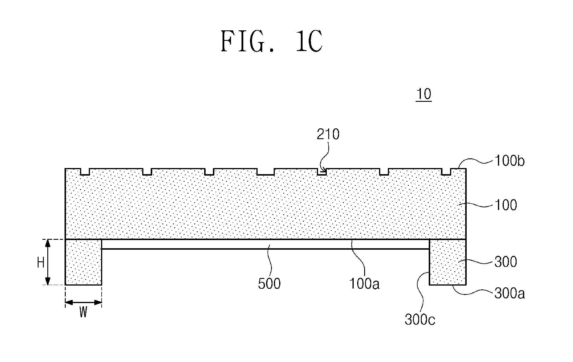
[0023] The first pad 100 may have a first surface 100a and a second surface 100b opposite to the first surface 100a. The second surface 100b of the first pad 100 may correspond to a top surface of the polishing pad 10 while the first surface 100a of the first pad 100 may correspond to a bottom surface of the polishing pad. The second surface 100b of the first pad 100 may serve as a polishing surface. For example, the second surface 100b of the first pad 100 may make contact with and polish the polishing target. The second surface 100b of the first pad 100 may be relatively rough, for example, the second surface 100b may be rougher than the first surface 100a. The first pad 100 may have a uniform thickness. For example, central and edge regions of the first pad 100 may have the same or similar maximum thickness. The second surface 100b of the first pad 100 may be straight and unbent. For example, the second surface 100b of the first pad 100 may have central and edge regions whose respective topmost portions are located at substantially the same level. The edge region of the second surface 100b of the first pad 100 may indicate a zone overlapped with the protrusion 300.
[0024] A plurality of grooves 210 may be disposed on the second surface 100b of the first pad 100. As illustrated in FIG. 1B, one or more of the plurality of grooves 210 may extend radially from a center of the polishing pad 10 toward an edge of the polishing pad 10. Others of the plurality of grooves 210 may be arranged in concentric circles. However, the present invention does not necessarily have this particular geometric configuration of grooves 210. For example, the grooves 210 may have spiral shapes. The planar shape of the grooves 210 may be arranged in various ways, all within the scope of the present disclosure. When a polishing process is performed, the grooves 210 may act as slurry paths through which the slurry may travel.
[0025] The protrusion 300 may be disposed on the first surface 100a of the first pad 100. The first surface 100a of the first pad 100 may be relatively flat. When viewed in plan as illustrated in FIG. 1A, the protrusion 300 may overlap with and extend up from an edge region of the first surface 100a of the first pad 100. The protrusion 300 may have a closed loop shape such as a ring shape. The protrusion 300 may expose a central region of the first surface 100a of the first pad 100. The protrusion 300 may have a height H equal to or greater than about 1 mm, for example, ranging from about 1 mm to about 100 mm, as may be seen in FIG. 1C. The protrusion 300 may have a bottom surface 300a at a different level from that of the first surface 100a of the first pad 100. For example, the bottom surface 300a of the protrusion 300 may be disposed at a lower level than that of the first surface 100a of the first pad 100. The protrusion 300 may have a width W ranging from about 2 mm to about 5 mm.
[0026] For example, the protrusion 300 and the first pad 100 may be integrally formed so as to constitute a single unitary body. The protrusion 300 and the first pad 100 may be connected to each other without a boundary, and may include the same material. The protrusion 300 may alternatively be formed by attaching a separate structure (e.g., a preliminary protrusion) onto the first surface 100a of the first pad 100. In this case, the protrusion 300 and the first pad 100 may include the same or different materials, and an adhesion may be used to attach the first pad 100 and the protrusion 300. The protrusion 300 may include a polymer, but the protrusion 300 may be formed of another material.
[0027] An adhesive layer 500 may further be disposed on the first surface 100a of the first pad 100. The first pad 100 may thus have the adhesive layer 500 attached onto an area of the first surface 100a that is not covered with the protrusion 300. The adhesive layer 500 may have a thickness that is less than the height H of the protrusion 300. The bottom surface 300a of the protrusion 300 may be located at a lower level than that of a bottom surface of the adhesive layer 500. The adhesive layer 500 may further extend along an inside surface 300c (e.g. inside facing sidewall) of the protrusion 300. The adhesive layer 500 may include a polymer.
[0028] FIG. 2 is a cross-sectional view taken along line I-II of FIG. 1A, showing a polishing pad according to exemplary embodiments of the present invention. It may be assumed that elements that are not described in detail below are at least similar to corresponding elements described above.
[0029] Referring to FIG. 2, a polishing pad 11 may include a protrusion 300, a first pad 100, and a second pad 200. The first pad 100 and the protrusion 300 may be at least similar to corresponding elements discussed above with reference to FIGS. 1A and 1B. The polishing pad 11 may have a first bottom surface and a second bottom surface respectively corresponding to a central region and an edge region in a plan view. The first bottom surface may correspond to the first surface 100a of the first pad 100, and the second bottom surface may correspond to the bottom surface 300a of the protrusion 300. The second bottom surface may be located at a lower level than that of the first bottom surface. The first pad 100 may be covered with the adhesive layer 500 on its first surface 100a (e.g., the first bottom surface) exposed by (e.g. not covered by) the protrusion 300. The second surface 100b of the first pad 100 may have central and edge regions whose respective topmost portions are located at the same or similar level. Differently from that shown FIGS. 1B and 1C, the second surface 100b of the first pad 100 might not serve as a polishing surface, and no grooves 210 are disposed in the first pad 100.
[0030] The second pad 200 may be disposed on the first pad 100. The second pad 200 may have a plurality of pores at least partially penetrating the second pad 200. The second pad 200 may include, for example, a polymer such as polyurethane. The second pad 200 may have a first surface facing the first pad 100 and a second surface 200b opposite to the first surface. The second surface 200b of the second pad 200 may correspond to a top surface of the polishing pad 11. The second surface 200b of the second pad 200 may serve as a polishing surface. A plurality of grooves 210 may be disposed on the second surface 200b of the second pad 200. The grooves 210 may have planar shapes and may be at least similar to the grooves 210 discussed above with reference to FIGS. 1B and 1C. Central and edge regions of the second pad 200 may have substantially the same maximum thickness as each other. The second surface 200b of the second pad 200 may have central and edge regions whose respective topmost portions are located at substantially the same level.
[0031] An adhesive pattern 150 may be interposed between the first pad 100 and the second pad 200. The second pad 200 may be attached through the adhesive pattern 150 to the first pad 100. The adhesive pattern 150 may include an insulating polymer. Central and edge regions of the adhesive pattern 150 may have substantially the same maximum thickness as each other.
[0032] FIG. 3A is a plan view illustrating a polishing pad according to exemplary embodiments of the present disclosure. FIG. 3B is a cross-sectional view taken along line I-II of FIG. 3A. It may be assumed that elements that are not described in detail below are at least similar to corresponding elements described above.
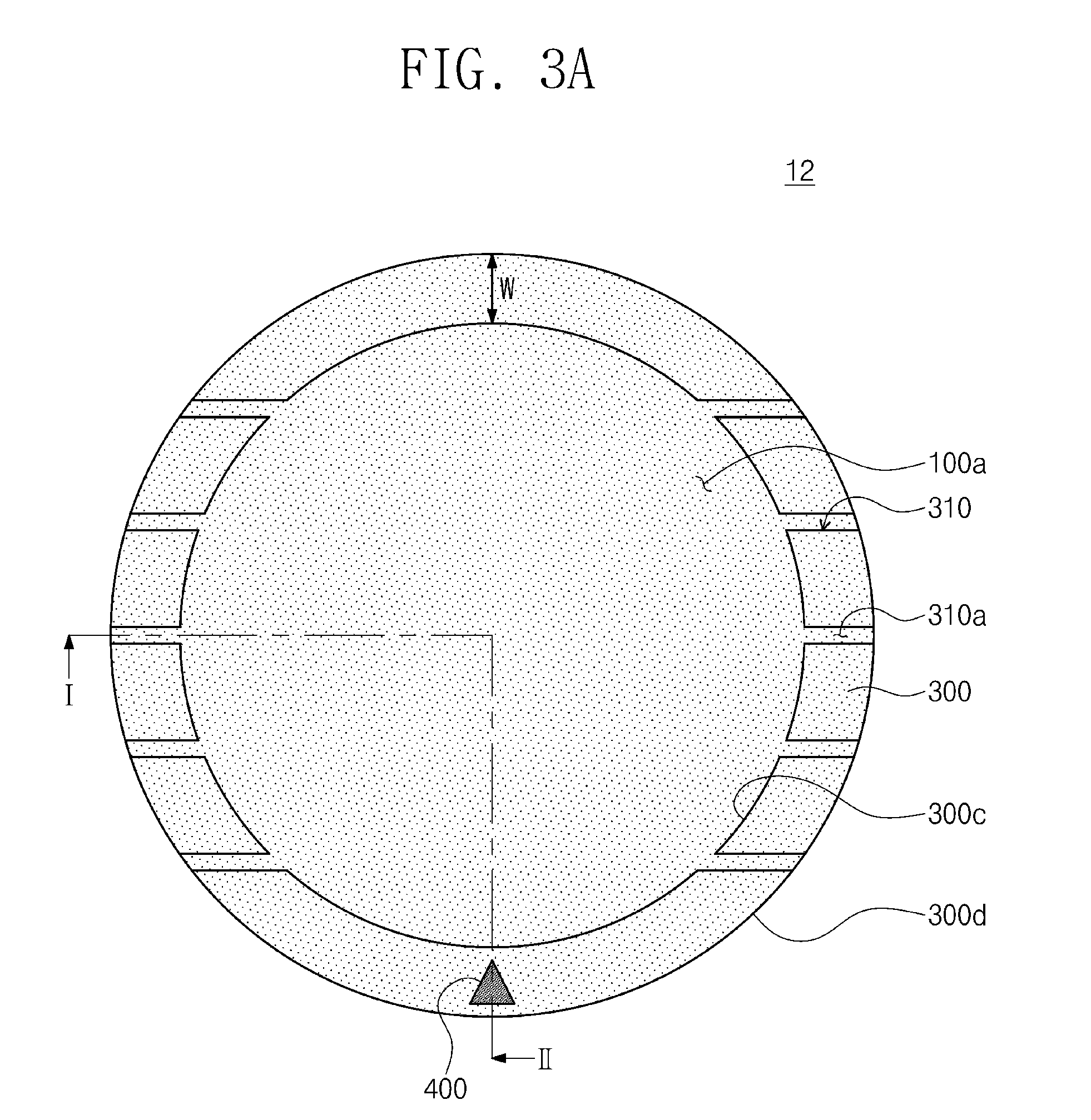
[0033] Referring to FIGS. 3A and 3B, a polishing pad 12 may include a first pad 100, a second pad 200, and a protrusion 300 disposed on the first pad 100. The first pad 100, the second pad 200, and the protrusion 300 may each be substantially the same as corresponding elements discussed above with reference to FIGS. 1A to 1C and 2. It is to be understood, however, that the adhesive pattern 150 and the second pad 200 are optional elements and may be omitted without departing from the scope of the present disclosure. As illustrated in FIGS. 1B and 1C, the grooves 210 may be disposed in the first pad 100. The protrusion 300 may have an inside surface 300c and an outside surface 300d opposite to each other. The inside and outside surfaces 300c and 300d of the protrusion 300 may extend in a direction intersecting the first surface 100a of the first pad 100.
[0034] A plurality of vent grooves 310 may be disposed in the protrusion 300. The vent grooves 310 may be disposed on and may penetrate the bottom surface 300a of the protrusion 300. As illustrated in FIG. 3B, the vent grooves 310 may have floor surfaces 310a at substantially the same level as that of the first surface 100a of the first pad 100. The floor surfaces 310a of the vent grooves 310 may be connected to the first surface 100a of the first pad 100. When viewed in plan, as illustrated in FIG. 3A, the vent grooves 310 may extend from the inside surface 300c of the protrusion 300 toward the outside surface 300d of the protrusion 300. For example, the vent grooves 310 may penetrate the inside and outside surfaces 300c and 300d of the protrusion 300. Alternatively, the vent grooves 310 may penetrate the inside surface 300c of the protrusion 300, but not the outside surface 300d of the protrusion 300. The number and planar shapes of the vent grooves 310 is not limited to the arrangements shown, and various different arrangements may be used, within the scope of the present disclosure.
[0035] The protrusion 300 may be formed on the first pad 100, and then the protrusion 300 may be partially removed to form the vent grooves 310. According to an exemplary embodiment of the present disclosure, the formation of the vent grooves 310 may include preparing a plurality of preliminary protrusions and attaching the preliminary protrusions onto the first surface 100a of the first pad 100 so as to be spaced apart from each other. In this case, the protrusion 300 may include a plurality of sub-protrusions spaced apart from each other, and the vent grooves 310 may be disposed between each of the plurality of sub-protrusions.
[0036] A mark 400 may further be disposed on the bottom surface 300a of the protrusion 300. The mark 400 may be a character or figure displayed on the bottom surface 300a of the protrusion 300. For example, the mark 400 may be formed by attaching a pattern onto the bottom surface 300a of the protrusion 300. Alternatively, the mark 400 may be a recession formed within the bottom surface 300a of the protrusion 300. A planar arrangement of the mark 400 is not limited to that shown, and various different arrangements are within the scope of the present disclosure.
[0037] The first pad 100 may include an adhesive layer 500 on its first surface 100a exposed by (e.g. not covered by) the protrusion 300. The adhesive layer 500 may further cover the inside surface 300c of the protrusion 300. An attaching process of the adhesive layer 500 and functions of the vent grooves 310 are described in greater detail below.
[0038] FIG. 3C is a cross-sectional view taken along line I-II of FIG. 3A, showing a method for attaching an adhesive layer according to exemplary embodiments of the present disclosure. It may be assumed that elements that are not described in detail below are at least similar to corresponding elements described above.
[0039] Referring to FIGS. 3A and 3C, the adhesive layer 500 may be disposed onto the first surface 100a of the first pad 100. In the process of attaching the adhesive layer 500, as indicated by an arrow in FIG. 3C, air may flow into the vent grooves 310 from between the adhesive layer 500 and the first pad 100. Air bubbles may then be reduced or prevented from being formed between the adhesive layer 500 and the first pad 100. The adhesive layer 500 may be sufficiently attached to the first pad 100. The mark 400 may signify an attachment direction in the process of attaching the adhesive layer 500. The attachment direction of the adhesive layer 500 may intersect the directions of extension of the vent grooves 310. Therefore, in the process of attaching the adhesive layer 500, air may be easily discharged through the vent grooves 310 to the outside.
[0040] A wafer polishing method according to exemplary embodiments of the present disclosure is described in detail below.
[0041] FIG. 4 is a flow chart illustrating a wafer polishing method according to exemplary embodiments of the present disclosure. FIG. 5 is a perspective view illustrating a wafer polishing method according to exemplary embodiments of the present disclosure. FIG. 6 is a cross-sectional view illustrating a polishing pad associated with a platen. It may be assumed that elements that are not described in detail below are at least similar to corresponding elements described above.
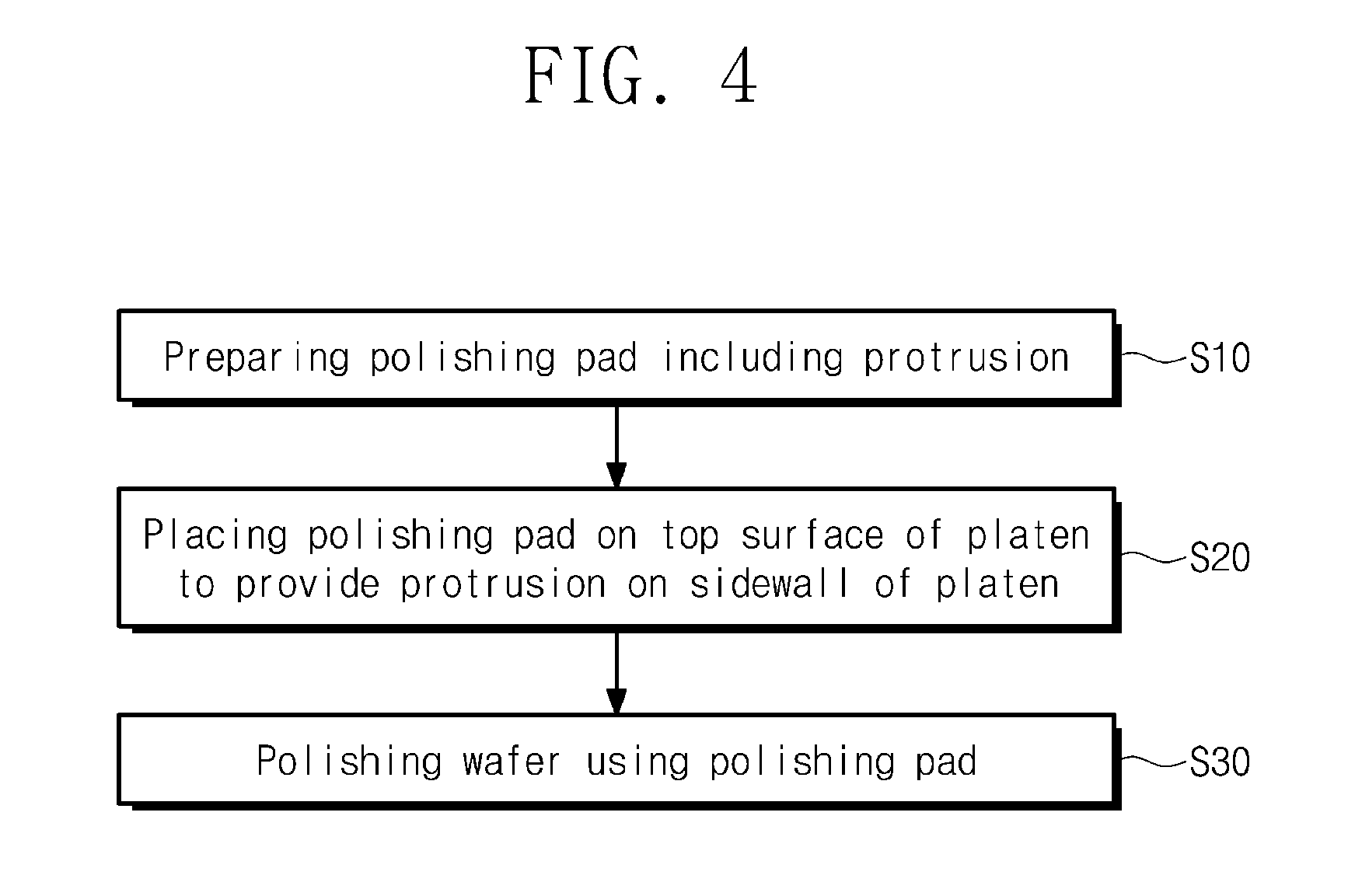
[0042] Referring to FIG. 4, one of the polishing pads 10, 11, and 12 including the protrusion 300 may be prepared (S10). For example, the polishing pad 10 discussed with reference to FIGS. 1A to 1C, the polishing pad 11 discussed with reference to FIG. 2, or the polishing pad 12 discussed with reference to FIGS. 3A and 3B may be prepared. The first pad 100 may include the adhesive layer 500 attached onto its first surface 100a exposed by (e.g. not covered by) the protrusion 300. For example, the attachment of the adhesive layer 500 may be performed at least similarly to that discussed above with reference to FIG. 3C. For convenience of description, a wafer polishing method using the polishing pad 11 of FIG. 2 will be described. According to exemplary embodiments of the present disclosure, a top surface of the polishing pad 11 may denote the second surface 200b of the second pad 200. When the polishing pad 10 of FIGS. 1A to 1C is used, the top surface of the polishing pad 11 may denote the second surface 100b of the first pad 100.
[0043] Referring to FIG. 5, a polishing apparatus may be prepared. The polishing apparatus may include a platen 1000, a wafer carrier 2000, a slurry supply 3000, and a pad conditioner 4000. The platen 1000 may have, for example, a cylindrical shape. The platen 1000 may receive power from a motor and the platen 1000 may be caused to rotate around its rotational axis. The rotational axis may be perpendicular to a top surface of the platen 1000.
[0044] Referring to FIGS. 4, 5, and 6, the polishing pad 11 may be placed on the top surface of the platen 1000 so as to cause the first surface 100a of the first pad 100 to face the top surface of the platen 1000 (S20). The polishing pad 11 may be attached through the adhesive layer 500 to the platen 1000. As illustrated in FIG. 6, the polishing pad 11 may have a diameter A1 greater than a diameter A2 of the platen 1000. The first pad 100 may have a diameter on its first surface 100a (e.g., the first bottom surface) exposed by (e.g. not covered by) the protrusion 300, and the diameter of the first surface 100a may be the same as or greater than the diameter A2 of the platen 1000. The protrusion 300 may be disposed on a sidewall 1000d of the platen 1000. The polishing pad 11 may then be precisely aligned with the platen 1000. For example, in a plan view, a central point of the polishing pad 11 may be aligned with a central point of the platen 1000. In addition, the polishing pad 11 and the platen 1000 may be aligned with each other at high speed to reduce process time. The protrusion 300 may more rigidly fix the polishing pad 11 to the platen 1000.
[0045] The polishing pad 11 may be used to polish a wafer WF (S30). In some exemplary embodiments of the present disclosure, the wafer WF may be prepared. The wafer carrier 2000 may use vacuum pressure to hold the wafer WF so as to cause a polishing target surface of the wafer WF to face the polishing pad 11. The wafer carrier 2000 may be driven to move up and down by an elevation unit. The wafer carrier 2000 may move downward to contact with the polishing pad 11 when a polishing process is performed. The wafer carrier 2000 may rotationally move to rotate the wafer WF during the polishing process.
[0046] The slurry supply 3000 may provide slurry onto the top surface of the polishing pad 11. A material of the slurry may be determined based on a kind and material of the polishing target surface of the wafer WF. The slurry may chemically polish the polishing target surface of the wafer WF, while contacting the polishing target surface of the wafer WF. For example, the polishing target surface of the wafer WF may change into an easily removable state due to reaction with the slurry.
[0047] The polishing pad 11 may be supported by and may rotate together with the platen 1000 during the polishing process. As discussed above, the pores of the first pad 100 or of the second pad 200 may receive the slurry. The polishing target surface of the wafer WF and the top surface of the polishing pad 11 may abrade against each other to mechanically polish the polishing target surface of the wafer WF. The grooves 210 may serve as paths for the slurry and polishing residues. When the central point of the polishing pad 11 is misaligned with the central point of the platen 1000, the slurry in the grooves 210 may move unintentionally. In some exemplary embodiments of the present disclosure, since the polishing pad 11 and the platen 1000 are accurately aligned with each other due to the protrusion 300, when the platen 1000 moves in rotary motion, the slurry may be evenly distributed in the grooves 210 and slurry residues may be satisfactorily discharged/removed from the grooves 210. As a result, the wafer WF may be evenly polished on its polishing target surface.
[0048] The pad conditioner 4000 may be installed adjacent to the platen 1000. The pad conditioner 4000 may move rotationally and reciprocally. The pad conditioner 4000 may contact the top surface of the polishing pad 11 and maintain an even surface roughness of the top surface of the polishing pad 11. Therefore, even though the polishing process is performed for a long time, the wafer WF may be satisfactorily polished on its polishing target surface.
[0049] When the diameter A1 of the polishing pad 11 is the same as or less than the diameter A2 of the platen 1000, the pad conditioner 4000 may come into contact with the platen 1000 (e.g., with an edge portion of the platen 1000) during the operation of the pad conditioner 4000. In this case, the pad conditioner 4000 and/or the platen 1000 may suffer from damage. In some exemplary embodiments of the present disclosure, the diameter A1 of the polishing pad 11 may be greater than the diameter A2 of the platen 1000. For example, the diameter A1 of the polishing pad 11 may be approximately 5 to 10 mm larger than the diameter A2 of the platen 1000. The pad conditioner 4000 and the platen 1000 may accordingly be prevented from colliding against each other.
[0050] When the diameter A1 of the polishing pad 11 is greater than the diameter A2 of the platen 1000, an edge portion of the polishing pad 11 might not be supported by the platen 1000. When no protrusion 300 is provided, edge portions of the first and second pads 100 and 200 may bend down lower than central portions of the first and second pads 100 and 200. For example, the edge portions not being supported by the platen 1000 may tend to bend inwardly toward the platen 1000. The top surface of the polishing pad 11 may thus be bent. The bending portion of the top surface of the polishing pad 11 may be excessively abraded by the pad conditioner 4000, with the result that the polishing pad 11 may decrease in life span. In some exemplary embodiments of the present disclosure, the polishing pad 11 may include the protrusion 300. The protrusion 300 may be disposed on the edge portion of the first pad 100. Hence, the edge portion of polishing pad 11 may be supported and this support may prohibit the first pad 100 from bending down. When the height H of the protrusion 300 is less than 1 mm, it may be unlikely that the protrusion 300 sufficiently prevents the bending of the polishing pad 11. In some exemplary embodiments of the present disclosure, the height H of the protrusion 300 may fall within a range equal to or greater than 1 mm, and thus the polishing pad 11 may be sufficiently prevented from bending. The polishing pad 11 may accordingly be prevented from being excessively abraded on its top surface. Thus, the polishing pad 11 may increase in life span.
[0051] According to exemplary embodiments of the present disclosure, a polishing pad may include a protrusion. The polishing pad may be disposed on the top surface of a platen. The protrusion may be disposed on the sidewall of the platen. The protrusion may accurately and quickly align the polishing pad with the platen. The process time may then decrease. The protrusion may rigidly fix the polishing pad to the platen.
[0052] The protrusion may prevent the polishing pad from bending down on the platen. The protrusion may suppress excessive abrasion of the polishing pad, and as a result, the polishing pad may increase in life span.
[0053] Exemplary embodiments described herein are illustrative, and many variations can be introduced without departing from the spirit of the disclosure or from the scope of the appended claims. For example, elements and/or features of different exemplary embodiments may be combined with each other and/or substituted for each other within the scope of this disclosure and appended claims.
* * * * *
D00000
D00001
D00002
D00003
D00004
D00005
D00006
D00007
D00008
D00009
XML
uspto.report is an independent third-party trademark research tool that is not affiliated, endorsed, or sponsored by the United States Patent and Trademark Office (USPTO) or any other governmental organization. The information provided by uspto.report is based on publicly available data at the time of writing and is intended for informational purposes only.
While we strive to provide accurate and up-to-date information, we do not guarantee the accuracy, completeness, reliability, or suitability of the information displayed on this site. The use of this site is at your own risk. Any reliance you place on such information is therefore strictly at your own risk.
All official trademark data, including owner information, should be verified by visiting the official USPTO website at www.uspto.gov. This site is not intended to replace professional legal advice and should not be used as a substitute for consulting with a legal professional who is knowledgeable about trademark law.