SRAM Configuration Cell for Low-Power Field Programmable Gate Arrays
Greene; Jonathan W. ; et al.
U.S. patent application number 16/178093 was filed with the patent office on 2019-06-06 for sram configuration cell for low-power field programmable gate arrays. This patent application is currently assigned to Microsemi SoC Corp.. The applicant listed for this patent is Microsemi SoC Corp.. Invention is credited to Jonathan W. Greene, John McCollum.
| Application Number | 20190172522 16/178093 |
| Document ID | / |
| Family ID | 66659509 |
| Filed Date | 2019-06-06 |

| United States Patent Application | 20190172522 |
| Kind Code | A1 |
| Greene; Jonathan W. ; et al. | June 6, 2019 |
SRAM Configuration Cell for Low-Power Field Programmable Gate Arrays
Abstract
A random-access memory cell includes first and second voltage supply nodes, first and second complementary output nodes, first and second complementary bit lines associated with the memory cell, and a word line associated with the memory cell. Pairs of series-connected cross-coupled p-channel and n-channel hybrid FinFET transistors are connected between the voltage supply nodes, the first bit line coupled to the first output node, and the second bit line coupled to the second output node.
| Inventors: | Greene; Jonathan W.; (Palo Alto, CA) ; McCollum; John; (Orem, UT) | ||||||||||
| Applicant: |
|
||||||||||
|---|---|---|---|---|---|---|---|---|---|---|---|
| Assignee: | Microsemi SoC Corp. San Jose CA |
||||||||||
| Family ID: | 66659509 | ||||||||||
| Appl. No.: | 16/178093 | ||||||||||
| Filed: | November 1, 2018 |
Related U.S. Patent Documents
| Application Number | Filing Date | Patent Number | ||
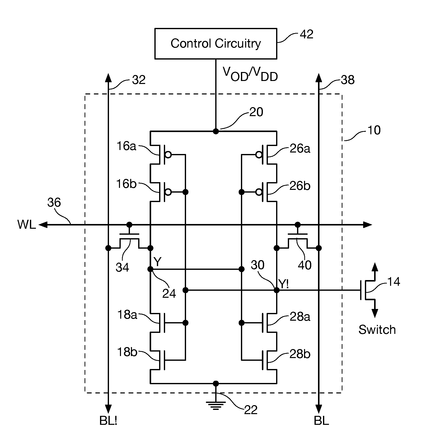
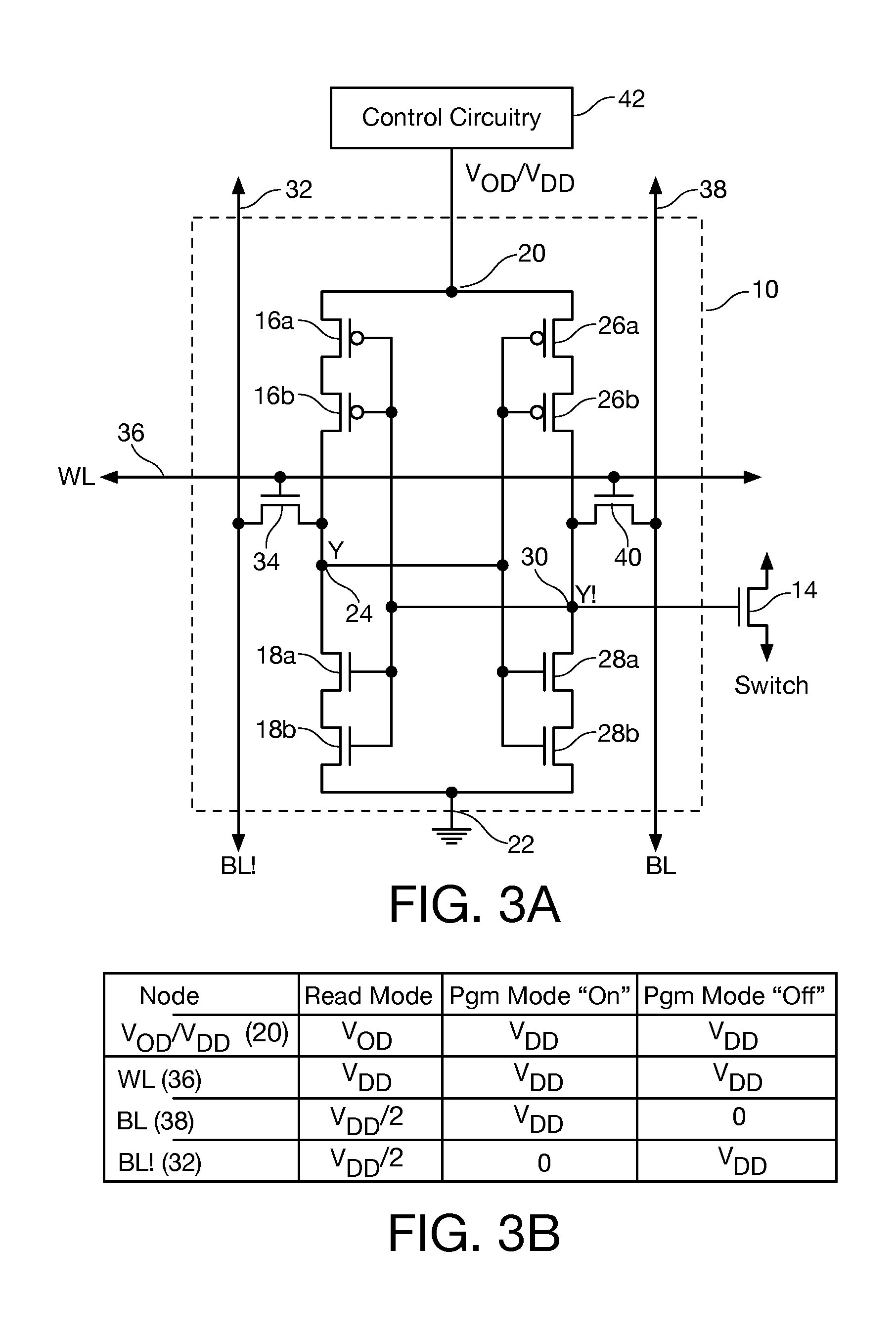
|---|---|---|---|---|
| 62594349 | Dec 4, 2017 | |||
| 62594481 | Dec 4, 2017 | |||
| Current U.S. Class: | 1/1 |
| Current CPC Class: | H03K 19/1776 20130101; G11C 11/419 20130101; G11C 11/412 20130101 |
| International Class: | G11C 11/412 20060101 G11C011/412; G11C 11/419 20060101 G11C011/419; H03K 19/177 20060101 H03K019/177 |
Claims
1. A random-access memory cell comprising: first and second voltage supply nodes; first and second complementary output nodes; first and second complementary bit lines associated with the memory cell; a word line associated with the memory cell; a first pair of series-connected p-channel hybrid FinFET transistors connected between the first power supply node and the first output node; a first pair of series-connected n-channel hybrid FinFET transistors connected between the first output node and the second power supply node; a second pair of series-connected p-channel hybrid FinFET transistors connected between the first power supply node and the first output node; a second pair of series-connected n-channel hybrid FinFET transistors connected between the first output node and the second power supply node; gates of the first pair of series-connected p-channel hybrid FinFET transistors and the first pair of series-connected n-channel hybrid FinFET transistors connected to the second output node; gates of the second pair of series-connected p-channel hybrid FinFET transistors and the second pair of series-connected n-channel hybrid FinFET transistors connected to the first output node; the first bit line coupled to the first output node, and the second bit line coupled to the second output node.
2. The random-access memory cell of claim 1 wherein: the first bit line is coupled to the first output node through a first n-channel FinFET select transistor; and the second bit line coupled to the second output node through a second re -channel hybrid FinFET select transistor.
3. The static random-access memory cell of claim 1 further comprising control circuitry configured to supply a programming potential to the first voltage supply node during a programming mode and supply an operating potential higher than the programming potential during a read mode.
4. The static random-access memory cell of claim 1 further comprising an re -channel hybrid FinFET switch transistor having a gate coupled to one of the first and second output nodes.
5. A static random-access memory cell comprising: first and second voltage supply nodes; first and second complementary output nodes; first and second complementary bit lines associated with the memory cell; a word line associated with the memory cell; a first pair of series-connected p-channel hybrid FinFET transistors connected between the first voltage supply node and the first output node; a first pair of series-connected n-channel hybrid FinFET transistors connected between the second voltage supply node and the first output node; a second pair of series-connected p-channel hybrid FinFET transistors connected between the first voltage supply node and the second output node; a second pair of series-connected n-channel hybrid FinFET transistors connected between the second voltage supply node and the second output node; the first pair of series-connected p-channel hybrid FinFET transistors and the first pair of series-connected n-channel hybrid FinFET transistors each having gates connected together to the second output node, and the second pair of series-connected p -channel hybrid FinFET transistors and the second pair of series-connected n-channel hybrid FinFET transistors each having gates connected together to the second output node; an n-channel hybrid FinFET transistor switch having a gate connected to one of the first and second output nodes; a first n-channel hybrid FinFET select transistor coupled between the first bit line and the first output node; a second n-channel hybrid FinFET select transistor coupled between the second bit line and the second output node; and the first and second n-channel hybrid FinFET select transistors each having a gate coupled to the word line.
6. The static random-access memory cell of claim 5 further comprising control circuitry configured to supply a programming potential to the first voltage supply node during a programming mode and supply an operating potential higher than the programming potential during a read mode.
7. The static random-access memory cell of claim 5 further comprising an re -channel hybrid FinFET switch transistor having a gate coupled to one of the first and second output nodes.
8. A method of operating a random-access memory cell formed from pairs of series-connected cross-coupled p-channel and n-channel hybrid FinFET transistors coupled to a pair of complementary bit lines through a pair of hybrid FinFET select transistors, the method comprising: during a programming mode of operation powering the memory cell with a first voltage potential and placing one of the first potential and 0V on a first one of the bit lines and the other one of the first potential and 0V on a second one of the bit lines; and during a read mode of operation powering the memory cell with a second voltage potential higher than the first voltage potential and placing half of the second voltage potential on both of the complementary bit lines.
9. The method of claim 8 further comprising: during the programming mode of operation selecting the memory cell for programming by placing the first voltage potential on gates of the pair of hybrid FinFET select transistors or deselecting the memory cell for programming by placing 0V on the gates of the pair of hybrid FinFET select transistors.
10. An integrated circuit comprising: a plurality of first random-access memory cells each including first and second voltage supply nodes, first and second complementary output nodes, first and second complementary bit lines associated with each first memory cell, and a word line associated with each first memory cell, each first memory cell further including pairs of series-connected cross-coupled p-channel and n-channel hybrid FinFET transistors connected between the voltage supply nodes, the first bit line coupled to the first output node, and the second bit line coupled to the second output node; and a plurality of second random-access memory cells each including first and second voltage supply nodes, first and second complementary output nodes, first and second complementary bit lines associated with each second memory cell, and a word line associated with each second memory cell, each second memory cell further including cross-coupled p-channel and n-channel hybrid FinFET transistors connected between the voltage supply nodes, the first bit line coupled to the first output node, and the second bit line coupled to the second output node.
11. The integrated circuit of claim 10, wherein: the first random-access memory cells each further comprise an n-channel hybrid FinFET switch transistor having a gate coupled to one of the first and second output nodes; and the second random-access memory cells each further comprise an n-channel hybrid FinFET switch transistor having a gate coupled to one of the first and second output nodes.
12. The integrated circuit of claim 10 further comprising control circuitry configured to supply a programming potential to the first voltage supply node plurality of the first random-access memory cells during a programming mode and supply an operating potential higher than the programming potential of the plurality of first random -access memory cells during a read mode.
Description
BACKGROUND
[0001] The present invention relates to user-programmable integrated circuits such as field programmable gate array integrated circuits. More particularly, the present invention relates to static random-access memory configuration cells for use in user-programmable integrated circuit devices such as field programmable gate array (FPGA) integrated circuits.
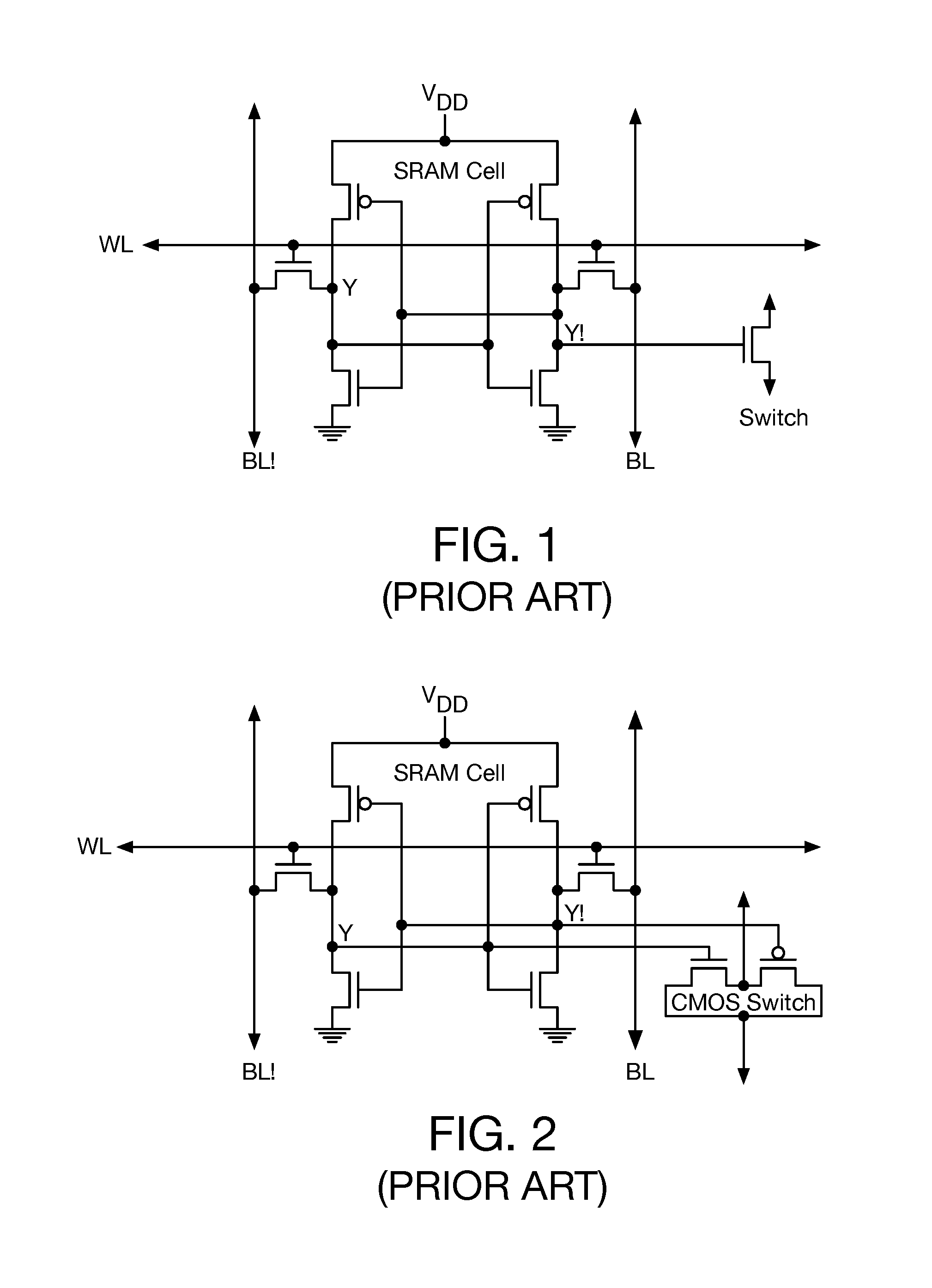
[0002] FIG. 1 shows a prior-art 6-transistor static random-access memory (SRAM) cell driving the gate of an n-channel switch transistor for use in a user-programmable integrated circuit such as an FPGA. The SRAM cell includes a first p-channel transistor in series with a first n-channel transistor between V.sub.DD and ground. The gates of the first p-channel transistor and the first n-channel transistor are connected together. The drains of the first p-channel transistor and the first n-channel transistor are connected together to define a first output node Y.
[0003] A second p-channel transistor is connected in series with a second n-channel transistor between V.sub.DD and ground, having their gates connected together. The drains of the second p-channel transistor and the second n-channel transistor are connected together to define a second output node Y!. The gates of the first p-channel and re -channel transistor are connected to the second output node Y! and the gates of the second p-channel and n-channel transistors are connected to the first output node Y. The type of memory cell depicted in FIG. 1 is sometimes referred to in the art as a cross-coupled memory cell.
[0004] The first node Y is coupled to a first bitline BL! associated with the memory cell through an n-channel transistor having its gate connected to a wordline WL associated with the memory cell. The second node Y! is coupled to a second bitline BL associated with the memory cell through an n-channel transistor having its gate connected to the wordline WL associated with the memory cell. The first and second bitlines BL!, BL are complementary.
[0005] The n-channel switch transistor switch has its gate connected to the second node Y! and is used to selectively connect one signal to another in the programmable routing of the FPGA, as controlled by the state of the SRAM cell. The transistors in the 6-transistor SRAM memory cell of FIG. 1 are all ordinary low-voltage transistors. The supply voltage is the normal logic supply voltage V.sub.DD.
[0006] There are a few drawbacks to the use of the memory cell of FIG. 1. First, the n -channel switch transistor cannot pass a full V.sub.DD voltage, but only V.sub.DD less a voltage V.sub.t, where V.sub.t is the threshold voltage of the n-channel switch transistor.
[0007] The n-channel switch transistor must have a relatively low V.sub.t in order to provide good speed. An undersirable consequence of using a transistor having a low V.sub.t is that the n-channel switch transistor will leak current from its source to drain terminals even when its gate is at ground and the device is shut off This unnecessarily contributes to the static power consumption of the FPGA.
[0008] One solution to these problems is to supply the SRAM cell with a voltage V.sub.OD selected to be higher than V.sub.DD so that the gate of the switch is over-driven to a voltage above V.sub.DD. To withstand the higher voltage, the planar transistor devices used in the SRAM cell are made having both a thicker gate oxide layer to provide a higher maximum V.sub.GS breakdown voltage for the higher gate voltages being encountered, and a longer channel to prevent punch-through at the higher drain to source voltages being encountered. The n-channel planar switch transistor driven by the SRAM cell uses a thicker oxide to withstand the voltages to which its gate will be subjected but still has the ordinary channel length because it is a low-voltage device. This solution to the prior art problem is described in Telikepalli, "Power vs. Performance: The 90 nm Inflection Point," Xilinx White Paper, 2006. This document is found at https://www.xilinx/com/support/documentation/white papers/wp223.pdf. As disclosed in Telikepalli, the gate oxide layer used in the switch transistor is thicker than the gate oxide layer used in the standard logic devices but still thinner than the gate oxide used in standard I/O devices, in order not to impact switching speed, meaning that it must be formed using an additional oxide formation step not present in the standard process flow.
[0009] This arrangement disclosed in Telikepalli addresses the three issues mentioned above, but introduces new problems. First, the long channel devices in the SRAM cell takes up extra die area on the integrated circuit. In addition, the need to provide a device having an additional medium-thickness oxide for the SRAM cell complicates the manufacturing process. As technology has advanced to feature sizes below 40 nm, and transistor geometry has evolved from planar geometry to FinFET geometry, it is no longer feasible to provide such non-standard medium thickness oxide devices. A reason for this is the advent of high-k gate processes such as the ones described in https://www.eecg.toronto.edu/.about.charlesc/chiasson fpl2013.pdf. Below 20 nm, when process technology changes from planar to FinFET transistors, it becomes even more difficult to continue to support a special non-standard medium-thickness oxide. As a result, at 20 nm FPGA manufacturers have started using CMOS transmission gates as switches. These do not require overdriving the gates to pass a full V.sub.DD.
[0010] FIG. 2 shows a prior-art 6-transistor static random-access memory (SRAM) cell identical to the SRAM memory cell shown in FIG. 1 driving the gates of an n-channel transistor switch and a p-channel transistor connected together to form a conventional CMOS transmission gate, also known as a pass-gate, for use in a user-programmable integrated circuit such as an FPGA. As in the SRAM memory cell of FIG. 1, the transistors are all ordinary low-voltage transistors. The use of a complementary pair of n -channel and p-channel transistors as the switch solves the problem of not passing a full V.sub.DD voltage. However, because a pair of devices instead of a single device is used, the area of the switch is increased, and the leakage is not improved. Furthermore, the need to bring both the true (Y) and complement (Y!) outputs of the SRAM cell to the switch devices requires a significant increase in layout area due to additional metal layer wiring requirements.
[0011] For a discussion of the tradeoffs of using pass-gates in FPGAs, see: http://www.eecg.toronto.edu/.about.charlesc/chiasson fpl2013.pdf
[0012] In summary, it would be very desirable to find a way to continue to use NMOS switches with overdriven gates but without making the process technology more complex and without increasing the area of the SRAM cell too much.
BRIEF DESCRIPTION
[0013] According to one aspect of the present invention, a random-access memory cell includes first and second voltage supply nodes, first and second complementary output nodes, first and second complementary bit lines associated with the memory cell, and a word line associated with the memory cell. Pairs of series-connected cross-coupled p -channel and n-channel hybrid FinFET transistors are connected between the voltage supply nodes, the first bit line coupled to the first output node, and the second bit line coupled to the second output node.
[0014] According to another aspect of the present invention, control circuitry coupled to the memory cell is configured to supply a programming potential to the first voltage supply node during a programming mode and supply an operating potential higher than the programming potential during an operating mode.
[0015] According to another aspect of the present invention, a method of operating a random-access memory cell formed from pairs of series-connected cross-coupled p -channel and n-channel hybrid FinFET transistors coupled to a pair of complementary bit lines through a pair of hybrid FinFET select transistors includes during a programming mode of operation powering the memory cell with a first voltage potential and placing one of the first potential and 0V on a first one of the bit lines and the other one of the first potential and 0V on a second one of the bit lines, and during a read mode of operation powering the memory cell with a second voltage potential higher than the first voltage potential and placing about half of the second voltage potential on both of the complementary bit lines.
[0016] According to another aspect of the present invention, an integrated circuit includes a plurality of first random-access memory cells each including first and second voltage supply nodes, first and second complementary output nodes, first and second complementary bit lines associated with each first memory cell, and a word line associated with each first memory cell. Each first memory cell further including pairs of series-connected cross-coupled p-channel and n-channel hybrid FinFET transistors connected between the voltage supply nodes, the first bit line coupled to the first output node, and the second bit line coupled to the second output node. A plurality of second random-access memory cells each including first and second voltage supply nodes, first and second complementary output nodes, first and second complementary bit lines associated with each first memory cell, and a word line associated with each first memory cell. Each second memory cell further including cross-coupled p-channel and n-channel hybrid FinFET transistors connected between the voltage supply nodes, the first bit line coupled to the first output node, and the second bit line coupled to the second output node.
BRIEF DESCRIPTION OF THE DRAWING FIGURES
[0017] The invention will be explained in more detail in the following with reference to embodiments and to the drawing in which are shown:
[0018] FIG. 1 is a schematic diagram of a prior-art SRAM memory cell;
[0019] FIG. 2 is a schematic diagram of another prior-art SRAM memory cell;
[0020] FIG. 3A is a schematic diagram of an SRAM configuration cell in accordance with one aspect of the present invention;
[0021] FIG. 3B is a table listing the potentials applied to the various nodes of the SRAM configuration cell of FIG. 3A in read mode (normal operating mode), and the two cases of programming mode;
[0022] FIG. 4 is a flow diagram showing an illustrative method in accordance with the present invention;
[0023] FIG. 5 is a diagram of an integrated circuit 70 having an illustrative arrangement of different SRAM memory cells in accordance with another aspect of the present invention.
DETAILED DESCRIPTION
[0024] Persons of ordinary skill in the art will realize that the following description of the present invention is illustrative only and not in any way limiting. Other embodiments of the invention will readily suggest themselves to such skilled persons.
[0025] Referring now to FIG. 3A, a 10-transistor static random-access memory (SRAM) configuration cell (shown within dashed region 10) driving the gate of an n-channel transistor switch 14 for use in a user-programmable integrated circuit such as an FPGA is shown. It is to be understand that a configuration cell does not require high speed switching, since the cell is set at initial configuration, and is generally not changed thereafter. The SRAM configuration cell 10 includes a first pair of series-connected p -channel FinFET transistors 16a and 16b in series with a first pair of series-connected re- channel FinFET transistors 18a and 18b disposed between two voltage supply rails 20 and 22. The drains of the second of the first pair of series-connected p-channel FinFET transistors 16b and the first of the first pair of series-connected n-channel FinFET transistors 18a are connected together to define a first output node Y at reference numeral 24.
[0026] A second pair of series-connected p-channel FinFET transistors 26a and 26b in series with a second pair of series-connected n-channel FinFET transistors 28a and 28b is disposed between the two power rails 20 and 22. The drains of the second of the second pair of series-connected p-channel FinFET transistors 26b and the first of the second pair of series-connected n-channel FinFET transistors 28a are connected together to define a second output node Y! at reference numeral 30.
[0027] The gates of the first pair of series-connected p-channel FinFET transistors 16a and 16b and the first pair of series-connected n-channel FinFET transistors 18a and 18b are connected to the second output node Y! at reference numeral 30. The gates of the second pair of series-connected p-channel FinFET transistors 26a and 26b and the second pair of series-connected n-channel FinFET transistors 28a and 28b are connected to the first output node Y at reference numeral 24. Like the memory cell of FIGS. 1 and 2, the arrangement of SRAM configuration cell 10 of FIG. 3 can be referred to as being cross -coupled.
[0028] The first output node Y at reference numeral 24 is coupled to a first bitline 32 (BL!) associated with the SRAM configuration cell 10 through an n-channel select transistor 34 having its gate connected to a wordline (WL) 36 associated with the SRAM configuration cell 10. The second output node Y! at reference numeral 30 is coupled to a second bitline 38 (BL) associated with the SRAM configuration cell 10 through an re -channel select transistor 40 having its gate connected to the wordline (WL) 36 associated with the SRAM configuration cell 10. The first and second bitlines BL! (32) and BL (38) are complementary.
[0029] The n-channel FinFET transistor switch 14 has its gate connected to the second node Y! (30) and is used to selectively connect one signal to another in the programmable routing of the FPGA, as controlled by the state of the SRAM configuration cell 10.
[0030] The p-channel and n-channel FinFET transistor devices 16a, 16b, 18a, 18b, 26a, 26b, 28a, and 28b are hybrid FinFET transistor devices. Hybrid FinFET transistor devices, as used herein, share three attributes: 1) they have the thick gate oxide layers of high-voltage input/output (I/O) devices; 2) they have the short channel geometries of ordinary low-voltage logic transistor FinFET devices; and 3) they have higher channel implant doses than the low-voltage FinFET devices in order to allow them to withstand the higher operating voltages without suffering from punch through. These hybrid FinFET transistor devices are disclosed in co-pending application Ser. No. 62/594,349, attorney Docket Number 17-33867, filed on the same date as the instant application and entitled "HYBRID HIGH-VOLTAGE LOW-VOLTAGE FINFET DEVICE". This co -pending application is incorporated by reference herein in its entirety, and the term "hybrid FinFET transistors" and "hybrid FinFET transistor devices" as used herein are intended to refer to the devices disclosed in the above-identified co-pending patent application.
[0031] The hybrid FinFET transistor devices used in the SRAM configuration cell 10 of the present invention can tolerate a voltage greater than V.sub.DD on their gates, yet are no larger than an ordinary low-voltage FinFET device. Unlike the prior-art FinFET devices, the hybrid FinFET devices used in the SRAM configuration cell 10 of the present invention do not require any additional "medium-thickness" gate oxide layers or other process changes, and as disclosed in the above-identified co-pending patent application, they may be fabricated using existing processes with the addition of only minimal adjustments to the process flow, mostly involving the geometry of the masks used in gate formation and channel implant steps of the fabrication process. The hybrid FinFET transistor device is especially suitable for use as a switch in a non-volatile memory user programmable circuit such as an FPGA, where adequate overdrive voltage is readily available from the non-volatile memory configuration cell.
[0032] As disclosed in the above-identified co-pending patent application, hybrid FinFET transistor devices can also be made having p-channel polarity. The goal is to have an SRAM configuration cell that can provide sufficient overdrive to use a hybrid switch device, but without complicating the manufacturing process with additional requirements for new devices. Furthermore, the SRAM configuration cell should consume as little die area as possible.
[0033] The first aspect of the invention is to form the SRAM configuration cell 10 from the same hybrid FinFET transistor devices used for the switch transistor 14. This avoids any need for a large spacing between the configuration bits and switches. The hybrid devices can withstand the elevated gate voltage due to their thick oxide. However the hybrid FinFET transistor devices still cannot withstand the source-drain voltages encountered in the memory cell itself without undue leakage that can otherwise inadvertently switch the state of the memory cell.
[0034] According to another aspect of the present invention, and as illustrated in the Table of FIG. 3B, exceeding V.sub.DD across the source and drain of the select transistors 34, 40 in the SRAM configuration cell 10 is avoided. During normal operating conditions (read mode) the memory cell 10 is powered by V.sub.OD, which can be, for example, 1.5V. During programming (write mode) the voltage powering the memory cell 10 is reduced to V.sub.DD, for example 0.8V to allow the use of a single transistor as select transistors 34 and 40. Prior to writing data to the SRAM configuration cell 10, control circuit 42 coupled to power rail 20 drops V.sub.OD to V.sub.DD, and then the SRAM configuration cell 10 is written to as usual by setting WL 36 and bitlines BL! 32 and BL 38 to appropriate voltages of 0 or V.sub.DD as known in the art. To program SRAM configuration cell 10 to turn on the hybrid FinFET transistor switch 14, control circuit 42 coupled to power rail 20 sets node 20 to V.sub.DD, WL 36 is set to V.sub.DD BL 38 is set to V.sub.DD and BL! 32 is set to 0V as shown in the table of FIG. 3B. To program SRAM configuration cell 10 to turn off the hybrid FinFET transistor switch 14, control circuit 42 coupled to power rail 20 sets node 20 to V.sub.DD, WL 36 is set to V.sub.DD, BL 38 is set to 0V and BL! 32 is set to V.sub.DD as also shown in the table of FIG. 3B.
[0035] During a read mode (normal operation) of the SRAM configuration cell 10 or other user-programmable circuit designed using the principles set forth herein, control circuit 42 sets the voltage on power rail 18 to V.sub.OD to overdrive the gate of switch transistor 14, but the bit lines 32 and 38 are maintained at V.sub.DD/2 to avoid undue leakage through the select devices as also shown in the table of FIG. 3B. Configuration and control of circuits such as control circuitry 42 is well known in the art.
[0036] This leaves only the remaining FINFET transistors in the SRAM configuration cell 10 exposed to source-drain voltages above V.sub.DD during normal circuit operation (i.e., read operation). To avoid this problem, two transistors 16a, 16b, 18a, 168, 26a, 26b, and 28a, 28b are provided in series in place of a single transistor shown in the prior art SRAM cell of FIG. 1. Thus V.sub.OD is divided across two off-state devices, and neither of the off -state devices sees a source-drain voltage in excess of V.sub.OD/2. During operation, with the bit lines at V.sub.DD/2, the SRAM configuration cell 10 can be supplied by V.sub.OD with no risk of exceeding the limit of any of the hybrid FINFET transistors 16a, 16b, 18a, 18b, 26a, 26b, 28a, 28b.
[0037] Referring now to FIG. 4, a flow diagram shows an illustrative method for operating an array of the memory cells of the present invention. The method starts at reference numeral 50.
[0038] At reference numeral 52 a command places the array in programming mode. This command is asserted at device powerup as well as at other selected times. At reference numeral 56, in response to the command placing the array in programming mode the voltage at the first voltage supply node is set at the programming voltage V.sub.DD. At reference numeral 58, a memory cell is selected and is programmed by asserting appropriate voltage potentials on the word lines and bit lines of the memory array. As indicated by decision diamond 60, cells are selected and programmed until all of the memory cells in the array have been programmed.
[0039] Next, at reference numeral 64, a command places the array in read mode, sometimes referred to as the "normal operating mode" of the memory cell. In response to the command placing the array in programming mode, the voltage at the first voltage supply node is set at the programming voltage V.sub.OD. The process ends at reference numeral 66.
[0040] Further in accordance with the present invention, user-programmable circuits such as FPGA circuits also require some configuration bits that do not drive switch gates, but instead drive logic inputs, and thus need not be driven by a voltage in excess of a V.sub.t above V.sub.DD. An example would be the 2 N bits used to configure an N-input LUT. Normally manufacturers prefer to use the same SRAM configuration cell for all purposes (including both controlling the switches and configuring the logic) to simplify the design and manufacturing. However in this context it is preferable to continue to use the smaller prior-art SRAM cell of FIG. 1 to drive the logic, and reserve use of the larger SRAM configuration cell 10 of FIG. 2 to those cases where it is necessary to overdrive switch gates.
[0041] Persons of ordinary skill in the art will appreciate that, because it is so important to minimize die area, providing two devices in series as in the SRAM configuration cell 10 is not the sort of thing that would typically be done in an SRAM configuration cell. However, the use of two different types of SRAM cells in the FPGA (the SRAM cell of FIG. 1 where possible and the SRAM configuration cell of FIG. 2 where necessary), the area savings from enabling the use of an NMOS hybrid switch instead of a CMOS switch, and reduction of the supply voltage to V.sub.DD during write operations to limit the source-drain voltage on the addressing devices and using pairs of series devices for the remaining devices in the SRAM cell can be acceptable as part of an overall solution for FPGA configuration.
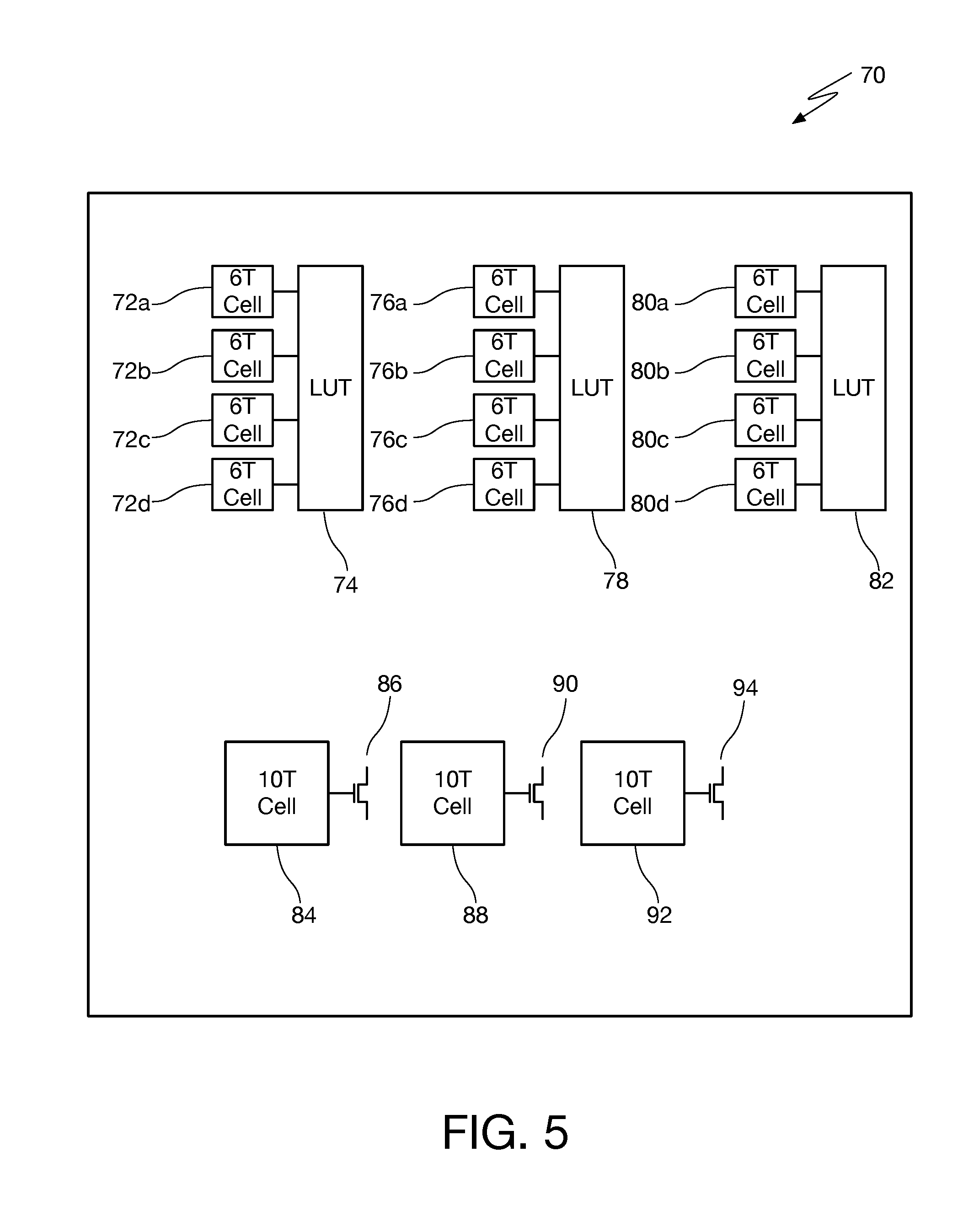
[0042] This aspect of the invention is shown in FIG. 5, a diagram of an integrated circuit 70 having an illustrative arrangement of different SRAM memory cells in accordance with the present invention. SRAM memory cells 72a, 72b, 72c, and 72d drive inputs to LUT 74. Similarly, SRAM memory cells 76a, 76b, 76c, and 76d drive inputs to LUT 78; and SRAM memory cells 80a, 80b, 80c, and 80d drive inputs to LUT 82. The inputs to LUTs 74, 78, and 82 are logic inputs that do not need to be overdriven. Accordingly, prior-art 6T SRAM cells such as those depicted in FIG. 1 can be employed.
[0043] SRAM configuration cell 84 drives n-channel switch transistor 86 Similarly, SRAM configuration cell 88 drives n-channel switch transistor 90; and SRAM configuration cell 92 drives n-channel switch transistor 86. The n-channel switch transistors 86, 90, and 94 connect circuit nets together and need to be overdriven to prevent a V.sub.t drop in the signal path. Consequently, the use of the SRAM configuration cell 10 of FIG. 3 is preferred to provide overdrive to the gates of the switch transistors 86, 90, and 94.
[0044] While embodiments and applications of this invention have been shown and described, it would be apparent to those skilled in the art that many more modifications than mentioned above are possible without departing from the inventive concepts herein. The invention, therefore, is not to be restricted except in the spirit of the appended claims.
* * * * *
References
D00000
D00001
D00002
D00003
D00004
XML
uspto.report is an independent third-party trademark research tool that is not affiliated, endorsed, or sponsored by the United States Patent and Trademark Office (USPTO) or any other governmental organization. The information provided by uspto.report is based on publicly available data at the time of writing and is intended for informational purposes only.
While we strive to provide accurate and up-to-date information, we do not guarantee the accuracy, completeness, reliability, or suitability of the information displayed on this site. The use of this site is at your own risk. Any reliance you place on such information is therefore strictly at your own risk.
All official trademark data, including owner information, should be verified by visiting the official USPTO website at www.uspto.gov. This site is not intended to replace professional legal advice and should not be used as a substitute for consulting with a legal professional who is knowledgeable about trademark law.