Methods For Forming A Transition Metal Nitride Film On A Substrate By Atomic Layer Deposition And Related Semiconductor Device S
Raisanen; Petri ; et al.
U.S. patent application number 16/245006 was filed with the patent office on 2019-05-30 for methods for forming a transition metal nitride film on a substrate by atomic layer deposition and related semiconductor device s. The applicant listed for this patent is ASM IP Holding B.V.. Invention is credited to Michael Eugene Givens, Petri Raisanen.
| Application Number | 20190164763 16/245006 |
| Document ID | / |
| Family ID | 62022567 |
| Filed Date | 2019-05-30 |


| United States Patent Application | 20190164763 |
| Kind Code | A1 |
| Raisanen; Petri ; et al. | May 30, 2019 |
METHODS FOR FORMING A TRANSITION METAL NITRIDE FILM ON A SUBSTRATE BY ATOMIC LAYER DEPOSITION AND RELATED SEMICONDUCTOR DEVICE STRUCTURES
Abstract
Methods for forming a transition metal nitride film on a substrate by atomic layer deposition and related semiconductor device structures are provided. In some embodiments, methods may include contacting a substrate with a first vapor phase reactant comprising a transition metal precursor and contacting the substrate with a second vapor phase reactant comprising an alkyl-hydrazine precursor. In some embodiments, related semiconductor device structures may include a PMOS transistor gate structure, the PMOS transistor gate structure including a transition metal nitride film and a gate dielectric between the transition nitride film and a semiconductor body. The transition metal nitride film includes a predominant (200) crystallographic orientation.
| Inventors: | Raisanen; Petri; (Gilbert, AZ) ; Givens; Michael Eugene; (Scottsdale, AZ) | ||||||||||
| Applicant: |
|
||||||||||
|---|---|---|---|---|---|---|---|---|---|---|---|
| Family ID: | 62022567 | ||||||||||
| Appl. No.: | 16/245006 | ||||||||||
| Filed: | January 10, 2019 |
Related U.S. Patent Documents
| Application Number | Filing Date | Patent Number | ||
|---|---|---|---|---|
| 15711989 | Sep 21, 2017 | 10229833 | ||
| 16245006 | ||||
| 62415842 | Nov 1, 2016 | |||
| Current U.S. Class: | 1/1 |
| Current CPC Class: | C23C 16/45527 20130101; H01L 21/823828 20130101; H01L 29/78 20130101; C23C 16/45553 20130101; H01L 29/4966 20130101; C23C 16/34 20130101; H01L 21/28088 20130101 |
| International Class: | H01L 21/28 20060101 H01L021/28; H01L 29/49 20060101 H01L029/49; C23C 16/455 20060101 C23C016/455; C23C 16/34 20060101 C23C016/34; H01L 21/8238 20060101 H01L021/8238; H01L 29/78 20060101 H01L029/78 |
Claims
1. A semiconductor device structure comprising: a PMOS transistor gate structure, the PMOS gate structure comprising: a transition metal nitride film; a semiconductor body; and a gate dielectric disposed between the transition metal nitride film and the semiconductor body; wherein the transition metal nitride film comprises a predominant (200) crystallographic orientation.
2. The semiconductor device structure of claim 1, wherein the transition metal nitride film comprises titanium nitride.
3. The semiconductor device structure of claim 1, wherein the transition metal nitride film has a thickness of less than approximately 50 Angstroms.
4. The semiconductor device structure of claim 1, wherein the PMOS gate structure has an effective work function greater than 4.2 eV.
5. The semiconductor device structure of claim 1, wherein the transition metal nitride film has atomic concentration of carbon greater than 0.5%.
6. A semiconductor device structure comprising: a NMOS transistor gate structure, the NMOS gate structure comprising: a transition metal nitride film; a semiconductor body; and a gate dielectric disposed between the transition metal nitride film and the semiconductor body; wherein the transition metal nitride film comprises a predominant (200) crystallographic orientation.
7. The semiconductor device structure of claim 6, wherein the transition metal nitride film comprises titanium nitride.
Description
[0001] CROSS-REFERENCE TO RELATED PATENT APPLICATIONS
[0002] The present application is a divisional of U.S. patent application Ser. No. 15/711,989, filed on Sep. 21, 2017 and entitled "METHODS FOR FORMING A TRANSITION METAL NITRIDE FILM ON A SUBSTRATE BY ATOMIC LAYER DEPOSITION AND RELATED SEMICONDUCTOR DEVICE STRUCTURES," which claims the benefit of U.S. Provisional Patent Application No. 62/415,842, filed on Nov. 1, 2016 and entitled "METHODS FOR FORMING A TRANSITION METAL NITRIDE FILM ON A SUBSTRATE BY ATOMIC LAYER DEPOSITION AND RELATED SEMICONDUCTOR DEVICE STRUCTURES," the disclosures of which are incorporated herein by reference.
BACKGROUND
Field of the Invention
[0003] The present disclosure relates generally to methods for forming a transition metal nitride film on a substrate by atomic layer deposition and related semiconductor device structures.
Description of the Related Art
[0004] Metal-oxide-semiconductor (MOS) technology has conventionally utilized n-type doped polysilicon as the gate electrode material. However, doped polysilicon may not be an ideal gate electrode material for advanced node applications. For example, although doped polysilicon is conductive, there may still be a surface region, which can be depleted of carriers under bias conditions. This region may appear as an extra gate insulator thickness, commonly referred to as gate depletion, and may contribute to the equivalent oxide thickness. While the gate depletion region may be thin, on the order of a few angstroms (.ANG.), it may become significant as the gate oxide thicknesses are reduced in advance node applications. As a further example, polysilicon does not exhibit an ideal effective work function (eWF) for both NMOS and PMOS devices. To overcome the non-ideal effective work function of doped polysilicon, a threshold voltage adjustment implantation may be utilized. However, as device geometries reduce in advanced node applications, the threshold voltage adjustment implantation processes may become increasingly complex and impractical.
[0005] To overcome the problems associated with doped polysilicon gate electrodes, the non-ideal doped polysilicon gate material may be replaced with an alternative material, such as, for example, a transition metal nitride. For example, the properties of a transition metal nitride may be modified to provide a gate electrode structure with a more ideal effective work function for both the NMOS and PMOS devices, where the effective work function of the gate electrode, i.e., the energy needed to extract an electron, must be compatible with the barrier height of the semiconductor material. For example, in the case of PMOS devices, the required effective work function is approximately 5.0 eV.
[0006] Atomic layer deposition (ALD) may be utilized for the deposition of transition metal nitride films, such as, for example, tantalum nitride (TaN), titanium nitride (TiN), tungsten nitride (WN) and niobium nitride (NbN). However, the modification of the electronic or crystallographic properties of ALD formed transition metal nitride films using known precursors may be limited due to the self-limiting nature of the ALD process.
SUMMARY
[0007] This summary is provided to introduce a selection of concepts in a simplified form. These concepts are described in further detail in the detailed description of example embodiments of the disclosure below. This summary is not intended to identify key features or essential features of the claimed subject matter, nor is it intended to be used to limit the scope of the claimed subject matter.
[0008] In some embodiments, methods for forming a transition metal nitride film on a substrate by atomic layer deposition are provided. The methods may comprise contacting the substrate with a first vapor phase reactant comprising a transition metal precursor and contacting the substrate with a second vapor phase reactant comprising an alkyl-hydrazine precursor.
[0009] In some embodiments, semiconductor device structures are provided. The semiconductor device structures may comprise a PMOS transistor gate structure, the PMOS transistor gate structure comprising a transition metal nitride film and a gate dielectric between the transition metal nitride film and a semiconductor body. In some embodiments, the transition metal nitride film comprises a predominant (200) crystallographic orientation.
[0010] For the proposes of summarizing the invention and the advantages achieved over the prior art, certain objects and advantages of the invention have been described herein above. Of course, it is to be understood that not necessarily all such objects or advantages may be achieved in accordance with any particular embodiment of the invention. Thus, for example, those skilled in the art will recognize that the invention may be embodied or carried out in a manner that achieves or optimizes one advantage or group of advantages as taught or suggested herein without necessarily achieving other objects or advantages as may be taught or suggested herein.
[0011] All of the embodiments are intended to be within the scope of the invention herein disclosed. These and other embodiments will become readily apparent to those skilled in the art from the following detailed description of certain embodiments having reference to attached figures, the invention not being limited to any particular embodiment(s) disclosed.
BRIEF DESCRIPTION OF THE DRAWINGS
[0012] While the specification concludes with claims particularly pointing out and distinctly claiming what are regarded as embodiments of the invention, the advantages of embodiments of the disclosure may be more readily ascertained from the description of certain examples of embodiments of the disclosure when read in conjunction with the accompanying drawings, in which:
[0013] FIG. 1 is a graph showing x-ray diffraction (XRD) scans of titanium nitride films formed according to the embodiments of the disclosure.
[0014] FIG. 2 is simplified cross section view of a semiconductor device structure formed according to the embodiments of the disclosure.
[0015] FIG. 3 is a graph showing the effective work function (eWF) of various gate electrode structures comprising a titanium nitride film as a function of titanium nitride film thickness.
[0016] FIG. 4 illustrates a reaction system configured to perform embodiments of the disclosure.
DETAILED DESCRIPTION
[0017] The illustrations presented herein are not meant to be actual view of any particular material, structure, or device, but are merely idealized representations that are used to describe embodiments of the disclosure.
[0018] As used herein, the term "atomic layer deposition" (ALD) may refer to a vapor deposition process in which deposition cycles, preferably a plurality of consecutive deposition cycles, are conducted in a process chamber. Typically, during each cycle the precursor is chemisorbed to a deposition surface (e.g., a substrate surface or a previously deposited underlying surface such as material from a previous ALD cycle), forming a monolayer or sub-monolayer that does not readily react with additional precursor (i.e., a self-limiting reaction). Thereafter, if necessary, a reactant (e.g., another precursor or reaction gas) may subsequently be introduced into the process chamber for use in converting the chemisorbed precursor to the desired material on the deposition surface. Typically, this reactant is capable of further reaction with the precursor. Further, purging steps may also be utilized during each cycle to remove excess precursor from the process chamber and/or remove excess reactant and/or reaction byproducts from the process chamber after conversion of the chemisorbed precursor. Further, the term "atomic layer deposition," as used herein, is also meant to include processes designated by related terms such as, "chemical vapor atomic layer deposition," "atomic layer epitaxy" (ALE), molecular beam epitaxy (MBE), gas source MBE, or organometallic MBE, and chemical beam epitaxy when performed with alternating pulses of precursor composition(s), reactive gas, and purge (e.g., inert carrier) gas.
[0019] As used herein, the term "substrate" may refer to any underlying material or materials that may be used, or upon which a device, a circuit or a film may be formed.
[0020] As used herein, the term "alkyl-hydrazine" may refer to a derivative of hydrazine (N.sub.2H.sub.4) which may comprise an alkyl functional group and may also comprise additional functional groups.
[0021] The present disclosure includes methods and device structures that may be used to form a transition metal nitride film or comprise a transition metal nitride film. The existing precursors that may be utilized in the ALD of transition metal nitride films may have limitations due to their inability to tune certain characteristics of the ALD transition metal nitride film; such characteristics may include the effective work function and the crystallographic orientation. For example, it is known that the effective work function of a gate electrode may vary as a function of its thickness, i.e., the effective work function of the gate electrode may decrease or increase with decreasing thickness of the materials comprising the gate electrode. As device geometries decrease in advanced node applications, the thickness of the corresponding device films, for example, such as the gate electrode, may also decrease with a corresponding change in the effective work function of the film. Such a change in the effective work function of the gate electrode at reduced thickness may result in a non-ideal effective work function for NMOS and PMOS device structures. Methods and structures are therefore required to provide a more desirable transition metal nitride film. Examples of such methods and structures are disclosed in further detail below.
[0022] ALD is based on typically self-limiting reactions, whereby sequential and alternating pulses of reactants are used to deposit about one atomic (or molecular) monolayer of material per deposition cycle. The deposition conditions and precursors are typically selected to provide self-saturating reactions, such that an adsorbed layer of one reactant leaves a surface termination that is non-reactive with the gas phase reactants of the same reactant. The substrate is subsequently contacted with a different reactant that reacts with the previous termination to enable continued deposition. Thus, each cycle of alternated pulses typically leaves no more than about one monolayer of the desired material. However, as mentioned above, the skilled artisan will recognize that in one or more ALD cycles more than one monolayer of material may be deposited, for example, if some gas phase reactions occur despite the alternating nature of the process.
[0023] In an ALD-type process for depositing transition metal nitride films, one deposition cycle comprises exposing the substrate to a first reactant, removing any unreacted first reactant and reaction byproducts from the reaction space, exposing the substrate to a second reactant, followed by a second removal step. The first reactant may comprise a metal precursor, in particular a transition metal precursor, such as a titanium precursor, and the second reactant may comprise an alkyl-hydrazine precursor, such as, for example, at least one of tertbutylhydrazine (C.sub.4H.sub.9N2H.sub.3), methylhydrazine (CH.sub.3NHNH.sub.2), dimethylhydrazine ((CH.sub.3).sub.2N.sub.2H.sub.2).
[0024] The transition metal precursor or compound may comprise at least one of the transition metals selected from the group comprising scandium (Sc), yttrium (Y), titanium (Ti), zirconium (Zr), hafnium (Hf), vanadium (V), niobium (Nb), tantalum (Ta), chromium (Cr), molybdenum (Mo), tungsten (W), manganese (Mn), technetium (Tc), rhenium (Re), iron (Fe), ruthenium (Ru), osmium (Os), cobalt (Co), rhodium (Rh), iridium (Ir), nickel (Ni), palladium (Pd), platinum (Pt), copper (Cu), silver (Ag), gold (Au), zinc (Zn), cadmium (Cd) or mercury (Hg). However, as titanium nitride films are exemplified herein, in such embodiments, the metal compound may comprise titanium.
[0025] As a non-limiting example embodiment, a transition metal halide reactant, such as, e.g., titanium tetrachloride (TiCl.sub.4), may be used as the transition metal precursor in ALD processes.
[0026] Precursors may be separated by inert gases, such as argon (Ar) or nitrogen (N.sub.2), to prevent gas-phase reactions between reactants and enable self-saturating surface reactions. In some embodiments, however, the substrate may be moved to separately contact a first metal reactant and a second alkyl-hydrazine reactant. Because the reactions self-saturate, strict temperature control of the substrates and precise dosage control of the precursors is not usually required. However, the substrate temperature is preferably such that an incident gas species does not condense into monolayers nor decompose on the surface. Surplus chemicals and reaction byproducts, if any, are removed from the substrate surface, such as by purging the reaction space or by moving the substrate, before the substrate is contacted with the next reactive chemical. Undesired gaseous molecules can be effectively expelled from a reaction space with the help of an inert purging gas. A vacuum pump may be used to assist in the purging.
[0027] According to some embodiments, ALD-type processes are used to form transition metal nitride films, for example, titanium nitride films on a substrate, such as an integrated circuit workpiece. Preferably, each ALD cycle comprises two distinct deposition steps or phases. In a first phase of the deposition cycle ("the metal phase"), the substrate surface on which deposition is desired is contacted with a first reactant comprising a transition metal such as titanium (i.e., titanium source material or chemical) which chemisorbs onto the substrate surface, forming no more than about one monolayer of reactant species on the surface of the substrate.
[0028] In some embodiments, the transition metal (e.g., titanium) source chemical, also referred to herein as the "transition metal compound" (or in some embodiments as the "titanium compound"), is a halide and the adsorbed monolayer is terminated with halogen ligands. In some embodiments, the titanium halide may be titanium tetrachloride (TiCl.sub.4).
[0029] Excess transition metal (e.g., titanium) source material and reaction byproducts (if any) may be removed from the substrate surface, e.g., by purging with an inert gas. Excess transition metal source material and any reaction byproducts may be removed with the aid of a vacuum generated by a pumping system.
[0030] In a second phase of the deposition cycle ("the nitrogen phase"), the substrate is contacted with an alkyl-hydrazine. In some embodiments the alkyl-hydrazine may comprise at least one of tertbutylhydrazine, methylhydrazine, dimethylhydrazine. The second alkyl-hydrazine reactant may react with the titanium-containing molecules left on the substrate surface. Preferably, in the second phase nitrogen is incorporated into the film by the interaction of the second alkyl-hydrazine reactant with the monolayer left by the transition metal (e.g., titanium) source material. In some embodiments, reaction between the second alkyl-hydrazine reactant and the chemisorbed transition metal species produces a transition metal nitride thin film over the substrate.
[0031] Excess second source chemical and reaction byproducts, if any, are removed from the substrate surface, for example by a purging gas pulse and/or vacuum generated by a pumping system. Purging gas is preferably any inert gas, such as, without limitation, argon (Ar), nitrogen (N.sub.2) or helium (He). A phase is generally considered to immediately follow another phase if a purge (i.e., purging gas pulse) or other reactant removal step intervenes.
[0032] FIG. 1 is a graph showing the 2 theta x-ray diffraction (XRD) scans of example titanium nitride films formed by ALD process of the current disclosure utilizing a transition metal precursor and an alkyl-hydrazine precursor. For example, the XRD scan denoted by the label 100 is taken from a titanium nitride film formed by ALD utilizing titanium tetrachloride and an alkyl-hydrazine at a substrate temperature of 350.degree. C. The XRD scan denoted by label 100 indicates that transition metal nitride films, such as, for example, titanium nitride, formed by the methods of the disclosure may comprise a number of crystallographic orientations including (111), (200), (220), (311) and (420) orientations with the (200) crystallographic orientation being predominant. Therefore, in some embodiments of the disclosure, the transition metal nitride film, formed by the ALD processes described herein, comprises a (200) crystallographic orientation and in some embodiments the transition metal nitride film comprises a predominant (200) crystallographic orientation.
[0033] In some embodiments of the disclosure, forming the transition metal nitride film may comprise forming the transition metal nitride film to a thickness of less than 50 Angstroms, or to a thickness of less than 30 Angstroms, or to a thickness of less than 20 Angstroms. As a non-limiting example embodiment of the disclosure, forming the transition metal nitride film may comprise forming a titanium nitride film to a thickness of less than 30 Angstroms.
[0034] The utilization of an alkyl-hydrazine precursor as the nitrogen source in the ALD processes described herein may allow for the formation of transition metal nitride films, such as titanium nitride, with an increased atomic percentage of carbon and hydrogen. The ability to incorporate increased atomic percentages of carbon and hydrogen into the transition metal nitride film may allow the ability to modify the characteristics of the ALD transition metal nitride film. For example, in some embodiments methods may comprise forming the transition metal nitride film to have an atomic concentration of carbon greater than 0.1%, or greater than 0.5%, or greater than 1%, or even greater than 10%. In addition, in some embodiments, methods may comprise forming the transition metal nitride film to have an atomic concentration of hydrogen greater than 0.1%, or greater than 1%, or greater than 2%, or even greater than 10%. In the embodiments outlined herein, the atomic concentration of an element may be determined utilizing Rutherford backscattering (RBS).
[0035] The ALD processes described herein, utilizing a transition metal precursor and an alkyl-hydrazine precursor, may be performed in an ALD deposition system with a heated substrate. For example, in some embodiments, methods may comprise heating the substrate to temperature of greater than 300.degree. C. In some embodiments, methods may comprise heating the substrate to temperature of greater than 350.degree. C. In other embodiments, methods may comprise heating the substrate to temperature of greater than 450.degree. C.
[0036] The deposition rate of the thin film by ALD, which is typically presented as A/pulsing cycle, depends on a number of factors including, for example, on the number of available reactive surface sites or active sites on the surface and bulkiness of the chemisorbing molecules. In some embodiments, the deposition rate of such films may range from about 0.1 to about 5.0 .ANG./pulsing cycle. In some embodiments, the deposition rate can be about 0.1, 0.2, 0.3, 0.5, 1.0, 1.5, 2.0, 2.5, 3.0, 3.5, 4.0, 4.5, or 5.0 .ANG./pulsing cycle.
[0037] The transition metal nitride thin films, such as titanium nitride thin films, formed by the ALD processes disclosed herein can be utilized in a variety of contexts, such as in the formation of gate electrode structures. One of skill in the art will recognize that the processes described herein are applicable to many contexts, including fabrication of PMOS transistors including planar devices as well as multiple gate transistors, such as FinFETs.
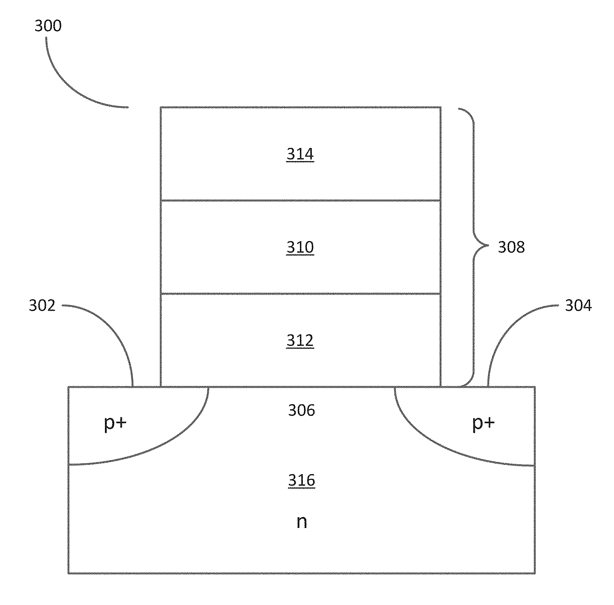
[0038] As a non-limiting example, and with reference to FIG. 2, a semiconductor device structure 300 may comprise a transistor structure and may include a source region 302, a drain region 304, a channel region 306 there between. A transistor gate structure 308 may comprise a gate electrode 310 which may be separated from the channel region 306 by a gate dielectric 312. According to the teaching of the present disclosure, the gate electrode 310 may comprise a transition metal nitride film, such as titanium nitride, formed by an atomic layer deposition process utilizing a transition metal precursor and an alkyl-hydrazine precursor. As shown in FIG. 2, in some embodiment the transistor gate structure 308 may further comprise one or more additional conductive layers 314 formed on the gate electrode 310. The one or more additional conductive layers 314 may comprise at least one of polysilicon, a refractory metal, a transition metal carbide, and a transition metal nitride.
[0039] In some embodiments, the semiconductor device structure 300 may comprise a PMOS transistor. The PMOS transistor may further comprise the transistor gate structure 308. The PMOS transistor gate structure 308 may comprise a gate electrode 310 comprising a transition metal nitride film and a gate dielectric 312 between the transition metal nitride film and a semiconductor body 316. In some embodiments, the semiconductor device structure 300 may comprise a NMOS transistor. The NMOS transistor may further comprise the transistor gate structure 308. The NMOS transistor gate structure 308 may comprise a gate electrode 310 comprising a transition metal nitride film and a gate dielectric 312 between the transition metal nitride film and a semiconductor body 316.
[0040] In some embodiments, the gate electrode 310, may comprise a transition metal nitride film, such as, for example, titanium nitride, tantalum nitride, tungsten nitride, and niobium nitride. In some embodiments the gate electrode 310, may comprise a transition metal nitride film, such as titanium nitride, and may comprise a predominant (200) crystallographic orientation.
[0041] In some embodiments of the disclosure, the additional conductive layers 314 may have an inherently lower effective work function and one of the purposes of the gate electrode 310 may be to modulate the effective work function of the transistor gate structure 308. For example, the effective work function of the additional conductive layers 314 may be approximately 4.2 eV and the gate electrode 310 may be utilized to modulate the effective work function of the transistor gate structure 308. In some embodiments, the properties (e.g., composition and thickness) of the gate electrode 310 may be adapted in order to controllably modulate the effective work function of the transistor gate structure 308 between approximately 4.2 eV and approximately 4.8 eV. As a non-limiting example embodiment, the thickness and the carbon content of the gate electrode 308 may be adapted to provide an optimized effective work function for an NMOS transistor structure. For example, in some embodiments of the disclosure, the gate electrode 310 may have a thickness of less than 10 Angstroms and a carbon content of less than 10%, which may result in an effective work function of the transistor gate structure 308 of approximately 4.6 eV.
[0042] In some embodiments of the disclosure, the properties of the gate electrode 310 may be tailored to controllably module the effective work function of the transistor gate structure 308 in order to effectively tune the threshold voltage (V.sub.th) of a PMOS transistor and/or an NMOS transistor. For example, the effective work function of the transistor gate structure may be varied in order to fabricate a complementary metal-oxide-semiconductor (CMOS) integrated circuit, comprising a plurality of NMOS transistors and PMOS transistors, with multiple threshold voltages (V.sub.th), commonly referred to as multi-threshold CMOS (MTCMOS).
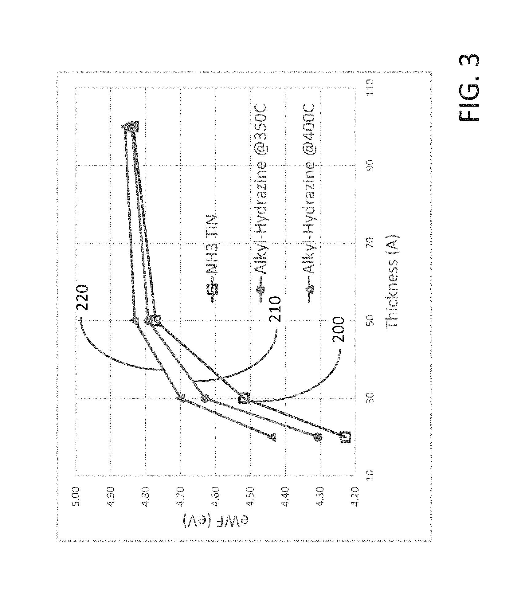
[0043] As a non-limiting example embodiment, FIG. 3 is a graph showing the effective work function (eWF) of various gate electrode structures comprising a titanium nitride film as a function of the titanium nitride film thickness. In these non-limiting example embodiments the gate electrode structure 308 comprises a hafnium oxide gate oxide 312, a titanium nitride gate electrode 310 and one or more additional conductive layers 314 comprising titanium aluminum carbide and titanium nitride.
[0044] The eWF line labelled as 200 indicates the eWF of a gate electrode structure comprising a titanium nitride film formed by ALD utilizing the common prior art precursor ammonia (NH.sub.3) as the nitrogen source. The eWF line labelled as 210 indicates the eWF of a gate electrode structure comprising a titanium nitride film formed by ALD processes as taught in the current disclosure, utilizing an alkyl-hydrazine as the nitrogen source, at a substrate temperature of 350.degree. C. The eWF line labelled as 220 indicates the eWF of a gate electrode structure comprising a titanium nitride film formed by ALD processes as taught in the current disclosure, utilizing an alkyl-hydrazine as the nitrogen source, at a substrate temperature of 400.degree. C. As shown in FIG. 3, the gate electrode structures comprising a titanium nitride film formed by the ALD processes of the current disclosure (i.e., utilizing an alkyl-hydrazine precursor) show a marked increase in eWF at reduced titanium nitride film thickness. For example, at a titanium nitride film thickness of approximately equal to or less than 20 Angstroms, the gate electrode structures comprising titanium nitride films formed utilizing the alkyl-hydrazine precursor show an increase in eWF of greater than 200 meV over the gate electrode structure comprising a titanium nitride film formed utilizing the prior art ammonia precursor.
[0045] Therefore, in some embodiments of the disclosure, forming the transition metal nitride film by ALD using a transition metal precursor and an alkyl-hydrazine precursor may comprise forming a gate electrode structure comprising the transition metal nitride film to have an effective work function greater than 4.2 eV, or even an effective work function greater than 4.4 eV. It should be noted that the embodiments of the disclosure allow for formation of gate electrode structures comprising thin metal nitrides films with increased effective work function, for example, in some embodiments methods may comprise forming a gate electrode structure comprising a transition metal nitride film with a thickness of less than 50 Angstroms with an effective work function of greater than 4.8 eV. In further embodiments, methods may comprise forming the gate electrode structure comprising a transition metal nitride film with a thickness of less than 30 Angstroms with an effective work function of greater than 4.7 eV. In yet further embodiments, methods may comprise forming the gate electrode structure to comprise a transition metal nitride film with a thickness of less than 20 Angstroms with an effective work function of greater than 4.4 eV.
[0046] As a non-limiting example, the transition metal nitride film comprising the gate electrode 310 may in some embodiment have a thickness of less than 50 Angstroms, or in some embodiments less than 30 Angstroms or even in some embodiments less than 20 Angstroms.
[0047] The properties of the gate electrode 310 may also be further modified by the ability to incorporate increased atomic percentages of carbon and hydrogen into the transition metal nitride film comprising the gate electrode 310. For example, in some embodiments the transition metal nitride film comprising the gate electrode 310 may have an atomic concentration of carbon greater than 0.1%, or greater than 1%, or even greater than 10%. In addition, in some embodiments, the transition metal nitride film comprising the gate electrode 100 may have an atomic concentration of hydrogen greater than 0.1%, or greater than 1%, or even greater than 10%. In the embodiments outlined herein, the atomic concentration of an element may be determined utilizing Rutherford backscattering (RB S).
[0048] Embodiments of the disclosure may also include a reaction system configured to perform the methods of the disclosure. In more detail, FIG.4 schematically illustrates a reaction system 400 including a reaction chamber 402 that further includes mechanism for retaining a substrate (not shown) under predetermined pressure, temperature, and ambient conditions, and for selectively exposing the substrate to various gases. A precursor reactant source 404 may be coupled by conduits or other appropriate means 404A to the reaction chamber 402, and may further couple to a manifold, valve control system, mass flow control system, or mechanism to control a gaseous precursor originating from the precursor reactant source 404. A precursor (not shown) supplied by the precursor reactant source 404, the reactant (not shown), may be liquid or solid under room temperature and standard atmospheric pressure conditions. Such a precursor may be vaporized within a reactant source vacuum vessel, which may be maintained at or above a vaporizing temperature within a precursor source chamber. In such embodiments, the vaporized precursor may be transported with a carrier gas (e.g., an inactive or inert gas) and then fed into the reaction chamber 402 through conduit 404A. In other embodiments, the precursor may be a vapor under standard conditions. In such embodiments, the precursor does not need to be vaporized and may not require a carrier gas. For example, in one embodiment the precursor may be stored in a gas cylinder. The reaction system 400 may also include additional precursor reactant sources, such as a precursor reactant source 406, which may also be coupled to the reaction chamber by conduits 406A as described above.
[0049] A purge gas source 408 may also be coupled to the reaction chamber 402 via conduits 408A, and selectively supplies various inert or noble gases to the reaction chamber 402 to assist with the removal of precursor gas or waste gasses from the reaction chamber. The various inert or noble gasses that may be supplied may originate from a solid, liquid or stored gaseous form.
[0050] The reaction system 400 of FIG. 4, may also comprise a system operation and control mechanism 410 that provides electronic circuitry and mechanical components to selectively operate valves, manifolds, pumps and other equipment included in the reaction system 400. Such circuitry and components operate to introduce precursors, purge gasses from the respective precursor sources 404, 406 and purge gas source 408. The system operation and control mechanism 410 also controls timing of gas pulse sequences, temperature of the substrate and reaction chamber, and pressure of the reaction chamber and various other operations necessary to provide proper operation of the reaction system 400. The operation and control mechanism 410 can include control software and electrically or pneumatically controlled valves to control flow of precursors, reactants and purge gasses into and out of the reaction chamber 402. The control system can include modules such as a software or hardware component, e.g., a FPGA or ASIC, which performs certain tasks. A module can advantageously be configured to reside on the addressable storage medium of the control system and be configured to execute one or more processes.
[0051] Those of skill in the relevant arts appreciate that other configurations of the present reaction system are possible, including different number and kind of precursor reactant sources and purge gas sources. Further, such persons will also appreciate that there are many arrangements of valves, conduits, precursor sources, and purge gas sources that may be used to accomplish the goal of selectively feeding gasses into reaction chamber 402. Further, as a schematic representation of a reaction system, many components have been omitted for simplicity of illustration, and such components may include, for example, various valves, manifolds, purifiers, heaters, containers, vents, and/or bypasses.
[0052] The example embodiments of the disclosure described above do not limit the scope of the invention, since these embodiments are merely examples of the embodiments of the invention, which is defined by the appended claims and their legal equivalents. Any equivalent embodiments are intended to be within the scope of this invention. Indeed, various modifications of the disclosure, in addition to those shown and described herein, such as alternative useful combination of the elements described, may become apparent to those skilled in the art from the description. Such modifications and embodiments are also intended to fall within the scope of the appended claims.
* * * * *
D00000
D00001
D00002
D00003
D00004
XML
uspto.report is an independent third-party trademark research tool that is not affiliated, endorsed, or sponsored by the United States Patent and Trademark Office (USPTO) or any other governmental organization. The information provided by uspto.report is based on publicly available data at the time of writing and is intended for informational purposes only.
While we strive to provide accurate and up-to-date information, we do not guarantee the accuracy, completeness, reliability, or suitability of the information displayed on this site. The use of this site is at your own risk. Any reliance you place on such information is therefore strictly at your own risk.
All official trademark data, including owner information, should be verified by visiting the official USPTO website at www.uspto.gov. This site is not intended to replace professional legal advice and should not be used as a substitute for consulting with a legal professional who is knowledgeable about trademark law.