Oxygen Treatment For Nitride Etching
Chen; Zhijun ; et al.
U.S. patent application number 15/792303 was filed with the patent office on 2019-04-25 for oxygen treatment for nitride etching. This patent application is currently assigned to Applied Materials, Inc.. The applicant listed for this patent is Applied Materials, Inc.. Invention is credited to Zhijun Chen, Jiayin Huang, Anchuan Wang.
| Application Number | 20190122865 15/792303 |
| Document ID | / |
| Family ID | 66169469 |
| Filed Date | 2019-04-25 |


| United States Patent Application | 20190122865 |
| Kind Code | A1 |
| Chen; Zhijun ; et al. | April 25, 2019 |
OXYGEN TREATMENT FOR NITRIDE ETCHING
Abstract
Exemplary methods for laterally etching silicon nitride may include flowing oxygen-containing plasma effluents into a processing region of a semiconductor processing chamber. A substrate positioned within the processing region may include a trench formed through stacked layers including alternating layers of silicon nitride and silicon oxide. The methods may include passivating exposed surfaces of the silicon nitride with the oxygen-containing plasma effluents. The methods may include flowing a fluorine-containing precursor into the remote plasma region while maintaining the flow of the oxygen-containing precursor. The methods may include forming plasma effluents of the fluorine-containing precursor and the oxygen-containing precursor. The methods may include flowing the plasma effluents into the processing region of the semiconductor processing chamber. The methods may also include laterally etching the layers of silicon nitride from sidewalls of the trench.
| Inventors: | Chen; Zhijun; (San Jose, CA) ; Wang; Anchuan; (San Jose, CA) ; Huang; Jiayin; (Fremont, CA) | ||||||||||
| Applicant: |
|
||||||||||
|---|---|---|---|---|---|---|---|---|---|---|---|
| Assignee: | Applied Materials, Inc. Santa Clara CA |
||||||||||
| Family ID: | 66169469 | ||||||||||
| Appl. No.: | 15/792303 | ||||||||||
| Filed: | October 24, 2017 |
| Current U.S. Class: | 1/1 |
| Current CPC Class: | H01L 21/02164 20130101; H01J 37/32422 20130101; C23C 16/401 20130101; C23C 16/45529 20130101; H01L 21/76879 20130101; H01L 27/11582 20130101; C23C 16/45553 20130101; H01L 21/31116 20130101; H01L 21/32137 20130101; H01L 21/0217 20130101; C23C 16/345 20130101 |
| International Class: | H01J 37/32 20060101 H01J037/32; C23C 16/34 20060101 C23C016/34; C23C 16/40 20060101 C23C016/40; C23C 16/455 20060101 C23C016/455; H01L 21/02 20060101 H01L021/02; H01L 21/3213 20060101 H01L021/3213; H01L 21/768 20060101 H01L021/768 |
Claims
1. An etching method comprising: flowing an oxygen-containing precursor into a remote plasma region of a semiconductor processing chamber; forming a plasma of the oxygen-containing precursor to produce oxygen-containing plasma effluents; flowing the oxygen-containing plasma effluents into a processing region of the semiconductor processing chamber, wherein a substrate is positioned within the processing region, and wherein the substrate comprises a trench formed through stacked layers including alternating layers of silicon nitride and silicon oxide; passivating exposed surfaces of the silicon nitride with the oxygen-containing plasma effluents; flowing a fluorine-containing precursor into the remote plasma region while maintaining the flow of the oxygen-containing precursor, wherein the passivating is performed for a first period of time prior to flowing the fluorine-containing precursor; forming plasma effluents of the fluorine-containing precursor and the oxygen-containing precursor; flowing the plasma effluents into the processing region of the semiconductor processing chamber; and laterally etching the layers of silicon nitride from sidewalls of the trench.
2. The etching method of claim 1, further comprising repeating the method for at least one additional cycle.
3. The etching method of claim 1, wherein the stacked layers comprise at least 50 layers of alternating layers of silicon nitride and silicon oxide, and wherein the trench is characterized by an aspect ratio of greater than or about 100:1.
4. The etching method of claim 1, wherein the lateral etching is performed at a temperature of between about -100.degree. C. and about 100.degree. C.
5. The etching method of claim 4, wherein the temperature is between about 0.degree. C. and about 50.degree. C.
6. The etching method of claim 1, wherein the lateral etching is performed at a chamber operating pressure of less than or about 1 Torr.
7. The etching method of claim 1, wherein the passivating is performed at a chamber operating pressure of greater than or about 1 Torr.
8. The etching method of claim 1, wherein the passivating oxidizes a portion of the silicon nitride.
9. (canceled)
10. The etching method of claim 10, wherein the first period of time is greater than or about one minute.
11. The etching method of claim 10, wherein the etching is performed for a second period of time greater than the first period of time.
12. The etching method of claim 1, wherein a layer of silicon nitride at an upper region of the trench and a layer of silicon nitride at a lower region of the trench differ in lateral etch amounts by less than about 2 nm.
13. An etching method comprising: flowing an oxygen-containing precursor into a first remote plasma region of a semiconductor processing chamber; forming a plasma of the oxygen-containing precursor to produce oxygen-containing plasma effluents; flowing the oxygen-containing plasma effluents into a processing region of the semiconductor processing chamber, wherein a substrate is positioned within the processing region, and wherein the substrate comprises a trench formed through stacked layers including alternating layers of silicon nitride and silicon oxide; passivating exposed surfaces of the silicon nitride with the oxygen-containing plasma effluents for a first period of time; subsequent the first period of time, flowing a fluorine-containing precursor into a second remote plasma region while maintaining the flow of the oxygen-containing precursor into the first remote plasma region; forming a plasma within the second remote plasma region to generate plasma effluents of the fluorine-containing precursor while continuing to form a plasma within the first remote plasma region to generate plasma effluents of the oxygen-containing precursor; flowing the plasma effluents of the fluorine-containing precursor and the plasma effluents of the oxygen-containing precursor into the processing region of the semiconductor processing chamber; and laterally etching the layers of silicon nitride from sidewalls of the trench.
14. The etching method of claim 13, further comprising repeating the method for at least one additional cycle.
15. The etching method of claim 13, wherein the first remote plasma region and the second remote plasma region are the same region of the semiconductor processing chamber.
16. The etching method of claim 13, wherein a bottom of the trench is at least partially oxidized along with the layers of silicon nitride, and wherein the bottom of the trench is etched less than or about 5 nm.
17. The etching method of claim 13, wherein a temperature within the semiconductor processing chamber during the etching method is greater than or about 0.degree. C.
18. The etching method of claim 13, wherein the first remote plasma region comprises a remote plasma system ("RPS") unit fluidly coupled with an inlet to the semiconductor processing chamber.
19. The etching method of claim 13, wherein the second remote plasma region comprises a capacitively-coupled plasma region physically separated from the processing region by at least one electrode of the capacitively-coupled plasma region.
20. (canceled)
Description
TECHNICAL FIELD
[0001] The present technology relates to semiconductor processes and equipment. More specifically, the present technology relates to laterally etching silicon nitride in vertical structures.
BACKGROUND
[0002] Integrated circuits are made possible by processes which produce intricately patterned material layers on substrate surfaces. Producing patterned material on a substrate requires controlled methods for removal of exposed material. Chemical etching is used for a variety of purposes including transferring a pattern in photoresist into underlying layers, thinning layers, or thinning lateral dimensions of features already present on the surface. Often it is desirable to have an etch process that etches one material faster than another facilitating, for example, a pattern transfer process. Such an etch process is said to be selective to the first material. As a result of the diversity of materials, circuits, and processes, etch processes have been developed with a selectivity towards a variety of materials.
[0003] Etch processes may be termed wet or dry based on the materials used in the process. A wet HF etch preferentially removes silicon oxide over other dielectrics and materials. However, wet processes may have difficulty penetrating some constrained trenches and also may sometimes deform the remaining material. Dry etches produced in local plasmas formed within the substrate processing region can penetrate more constrained trenches and exhibit less deformation of delicate remaining structures. However, local plasmas may damage the substrate through the production of electric arcs as they discharge.
[0004] Thus, there is a need for improved systems and methods that can be used to produce high quality devices and structures. These and other needs are addressed by the present technology.
SUMMARY
[0005] Exemplary methods for laterally etching silicon nitride may include flowing an oxygen-containing precursor into a remote plasma region of a semiconductor processing chamber. The methods may include forming a plasma of the oxygen-containing precursor to produce oxygen-containing plasma effluents. The methods may include flowing the oxygen-containing plasma effluents into a processing region of the semiconductor processing chamber. A substrate positioned within the processing region may include a trench formed through stacked layers including alternating layers of silicon nitride and silicon oxide. The methods may include passivating exposed surfaces of the silicon nitride with the oxygen-containing plasma effluents. The methods may include flowing a fluorine-containing precursor into the remote plasma region while maintaining the flow of the oxygen-containing precursor. The methods may include forming plasma effluents of the fluorine-containing precursor and the oxygen-containing precursor. The methods may include flowing the plasma effluents into the processing region of the semiconductor processing chamber. The methods may also include laterally etching the layers of silicon nitride from sidewalls of the trench.
[0006] In some embodiments the methods may also include repeating the method for at least one additional cycle. The stacked layers may include at least 50 layers of alternating layers of silicon nitride and silicon oxide, and the trench may be characterized by an aspect ratio of greater than or about 100:1. The lateral etching may be performed at a temperature within the processing chamber of between about -100.degree. C. and about 100.degree. C. The temperature may be between about 0.degree. C. and about 50.degree. C. The lateral etching may be performed at a chamber operating pressure of less than or about 1 Torr. The passivating may be performed at a chamber operating pressure of greater than or about 1 Torr. The passivating may oxidize a portion of the silicon nitride. The passivating may be performed for a first period of time prior to flowing the fluorine-containing precursor. The first period of time may be greater than or about one minute. The etching may be performed for a second period of time greater than the first period of time. A layer of silicon nitride at an upper region of the trench and a layer of silicon nitride at a lower region of the trench may differ in lateral etch amounts by less than about 2 nm.
[0007] The present technology may also encompass additional etching methods. The methods may include flowing an oxygen-containing precursor into a first remote plasma region of a semiconductor processing chamber. The methods may include forming a plasma of the oxygen-containing precursor to produce oxygen-containing plasma effluents. The methods may include flowing the oxygen-containing plasma effluents into a processing region of the semiconductor processing chamber. A substrate may be positioned within the processing region, and the substrate may include a trench formed through stacked layers including alternating layers of silicon nitride and silicon oxide. The methods may include passivating exposed surfaces of the silicon nitride with the oxygen-containing plasma effluents for a first period of time. The methods may include, subsequent the first period of time, flowing a fluorine-containing precursor into a second remote plasma region while maintaining the flow of the oxygen-containing precursor into the first remote plasma region. The methods may include forming a plasma within the second remote plasma region to generate plasma effluents of the fluorine-containing precursor while continuing to form a plasma within the first remote plasma region to generate plasma effluents of the oxygen-containing precursor. The methods may include flowing the plasma effluents of the fluorine-containing precursor and the plasma effluents of the oxygen-containing precursor into the processing region of the semiconductor processing chamber. The methods may also include laterally etching the layers of silicon nitride from sidewalls of the trench.
[0008] In some embodiments, the methods may further include repeating the method for at least one additional cycle. The first remote plasma region and the second remote plasma region may be the same region of the semiconductor processing chamber. A bottom of the trench may be at least partially oxidized along with the layers of silicon nitride, and the bottom of the trench may be etched less than or about 5 nm. A temperature within the semiconductor processing chamber during the etching method may be greater than or about 0.degree. C. The first remote plasma region may include a remote plasma system ("RPS") unit fluidly coupled with an inlet to the semiconductor processing chamber. The second remote plasma region may include a capacitively-coupled plasma region physically separated from the processing region by at least one electrode of the capacitively-coupled plasma region.
[0009] The present technology may also encompass additional etching methods. The methods may include flowing deposition precursors into a processing region of a semiconductor processing chamber. A substrate may be positioned within the processing region, and the substrate may include a trench formed through stacked layers including alternating layers of silicon nitride and silicon oxide. The methods may include forming a sacrificial layer over the silicon nitride with the deposition precursors. The methods may include, subsequent forming the sacrificial layer, flowing a fluorine-containing precursor and an oxygen-containing precursor into a remote plasma region of the semiconductor processing chamber. The methods may include forming a plasma within the remote plasma region to generate plasma effluents of the fluorine-containing precursor and the oxygen-containing precursor. The methods may include flowing the plasma effluents into the processing region of the semiconductor processing chamber. The methods may also include laterally etching the layers of silicon nitride from sidewalls of the trench with the plasma effluents.
[0010] Such technology may provide numerous benefits over conventional systems and techniques. For example, the processes may provide finely reduced layers within a memory hole. Additionally, the operations of some embodiments of the present technology may all be performed in a single chamber. These and other embodiments, along with many of their advantages and features, are described in more detail in conjunction with the below description and attached figures.
BRIEF DESCRIPTION OF THE DRAWINGS
[0011] A further understanding of the nature and advantages of the disclosed technology may be realized by reference to the remaining portions of the specification and the drawings.
[0012] FIG. 1 shows a top plan view of one embodiment of an exemplary processing system according to embodiments of the present technology.
[0013] FIG. 2A shows a schematic cross-sectional view of an exemplary processing chamber according to embodiments of the present technology.
[0014] FIG. 2B shows a detailed view of a portion of the processing chamber illustrated in
[0015] FIG. 2A according to embodiments of the present technology.
[0016] FIG. 3 shows a bottom plan view of an exemplary showerhead according to embodiments of the present technology.
[0017] FIG. 4 shows exemplary operations in a method according to embodiments of the present technology.
[0018] FIG. 5 shows exemplary operations in a method according to embodiments of the present technology.
[0019] FIGS. 6A-6C show cross-sectional views of substrates being processed according to embodiments of the present technology.
[0020] Several of the figures are included as schematics. It is to be understood that the figures are for illustrative purposes, and are not to be considered of scale unless specifically stated to be of scale. Additionally, as schematics, the figures are provided to aid comprehension and may not include all aspects or information compared to realistic representations, and may include superfluous or exaggerated material for illustrative purposes.
[0021] In the appended figures, similar components and/or features may have the same reference label. Further, various components of the same type may be distinguished by following the reference label by a letter that distinguishes among the similar components. If only the first reference label is used in the specification, the description is applicable to any one of the similar components having the same first reference label irrespective of the letter.
DETAILED DESCRIPTION
[0022] In transitioning from 2D NAND to 3D NAND, many process operations are modified from vertical to horizontal operations. Additionally, as 3D NAND structures grow in the number of cells being formed, the aspect ratios of memory holes and other structures increase, sometimes dramatically. During 3D NAND processing, stacks of placeholder layers and dielectric materials may form the inter-electrode dielectric or IPD layers. These placeholder layers may have a variety of operations performed to place structures before fully removing the material and replacing it with metal. While the metallization may be incorporated on one side of the cell structure, operations may have previously been performed on the other side of the structure, such as forming floating gates or charge-trap layers. Although these layers may be formed within the memory hole, crosstalk between vertically separated memory cells may occur. One way to reduce this communication may include etching the placeholder material before forming these layers to allow dielectric material to further separate the individual cell material layers from adjacent cells.
[0023] Because of the high aspect ratios of these memory holes, penetrating the entire length to access cells at the bottom of the hole may be difficult. Conventional dry etch techniques may have difficulty with adequate diffusion of precursors to the bottom of the memory hole.
[0024] Accordingly, the etchants often begin etching the top cell layers before even reaching the bottom cell layers, which may not occur or may occur to only a limited degree. This may end up producing a V-shape through the memory holes where substantial etching may have occurred at placeholder materials at or near the top of the memory hole, and minimal and sometimes no etching has been performed at or near the bottom of the memory hole. Accordingly, many conventional technologies utilize a wet etch to access each of the cell placeholder materials to perform a lateral etch of placeholders before forming layers, such as the charge-trap layer. However, wet etching may be more robust than other etching techniques, and the wet etching may etch the placeholder materials further than necessary or desired. For example, the wet etching may etch each layer significantly, and may etch each layer almost through completely to other memory holes, which may make placing the cell layers in the appropriate or desired location more difficult, and may weaken the structures causing deformation. Additionally, as structures continue to shrink in size, the surface tension of fluids used in wet etching can cause pattern collapse or sticking issues.
[0025] The present technology overcomes these issues by performing a dry etch process that allows precursors to diffuse adequately through the cell materials before substantial etching has occurred at the upper regions of the cell. By producing a passivation or sacrificial layer, etching of nitride may be slowed to the point where full diffusion through the memory hole may occur to allow more uniform etching. Thus, a similar etching profile may be formed through placeholder materials at the top of the memory hole and the bottom of the memory hole, which may allow uniformly sized cells to be produced throughout the vertical stack, unlike other dry etch techniques. Additionally, the entire process may be performed in a single chamber depending on the operations performed, unlike wet etch techniques that require transferring the processed substrate between multiple chambers to perform the wet etch and then dry the substrate.
[0026] Although the remaining disclosure will routinely identify specific etching processes utilizing the disclosed technology, it will be readily understood that the systems and methods are equally applicable to deposition and cleaning processes as may occur in the described chambers. Accordingly, the technology should not be considered to be so limited as for use with etching processes or chambers alone. Moreover, although an exemplary chamber is described to provide foundation for the present technology, it is to be understood that the present technology can be applied to virtually any semiconductor processing chamber that may allow the single-chamber operations described.
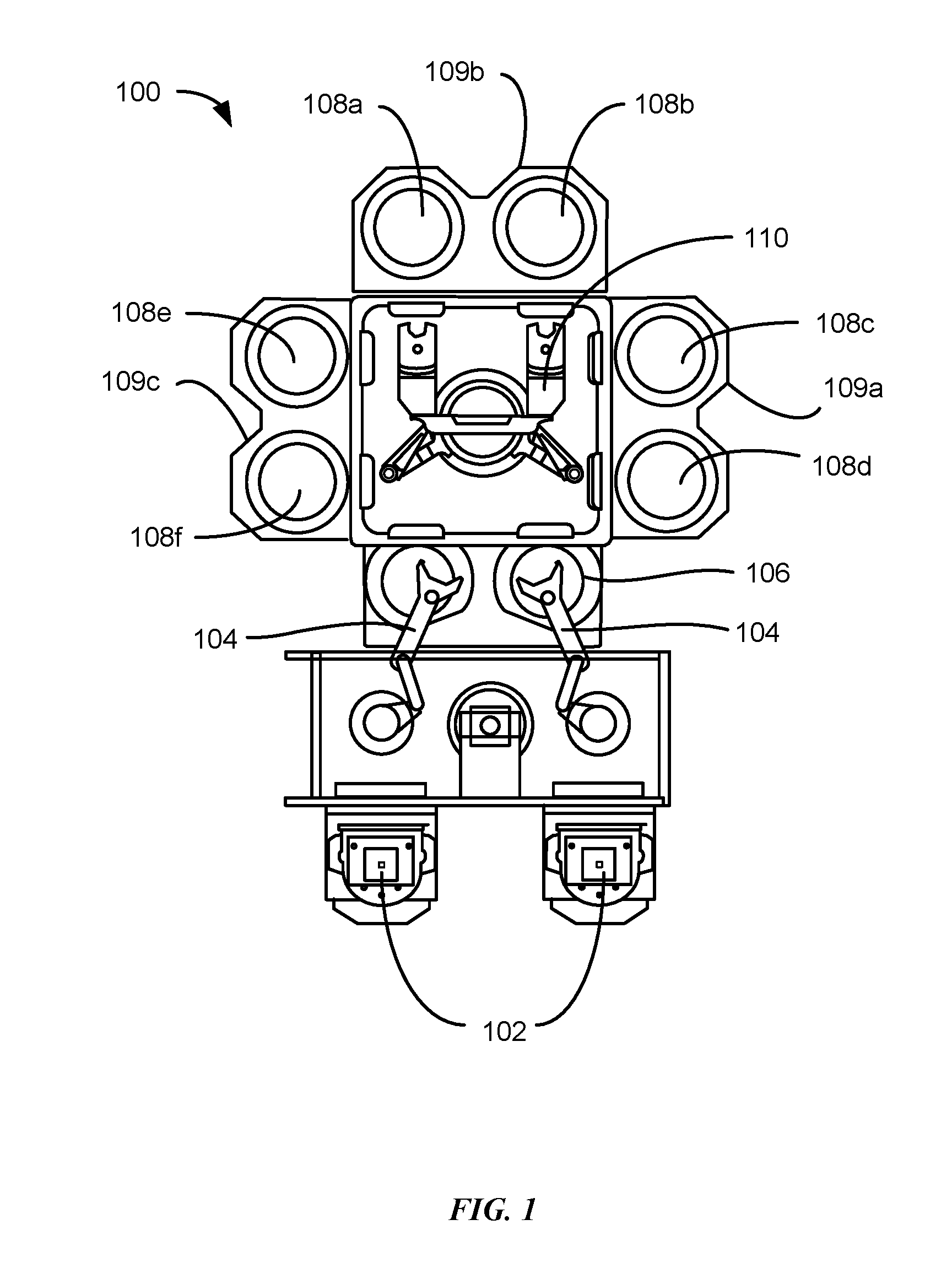
[0027] FIG. 1 shows a top plan view of one embodiment of a processing system 100 of deposition, etching, baking, and curing chambers according to embodiments. In the figure, a pair of front opening unified pods (FOUPs) 102 supply substrates of a variety of sizes that are received by robotic arms 104 and placed into a low pressure holding area 106 before being placed into one of the substrate processing chambers 108a-f, positioned in tandem sections 109a-c. A second robotic arm 110 may be used to transport the substrate wafers from the holding area 106 to the substrate processing chambers 108a-f and back. Each substrate processing chamber 108a-f, can be outfitted to perform a number of substrate processing operations including the dry etch processes described herein in addition to cyclical layer deposition (CLD), atomic layer deposition (ALD), chemical vapor deposition (CVD), physical vapor deposition (PVD), etch, pre-clean, degas, orientation, and other substrate processes.
[0028] The substrate processing chambers 108a-f may include one or more system components for depositing, annealing, curing and/or etching a dielectric film on the substrate wafer. In one configuration, two pairs of the processing chambers, e.g., 108c-d and 108e-f, may be used to deposit dielectric material on the substrate, and the third pair of processing chambers, e.g., 108a-b, may be used to etch the deposited dielectric. In another configuration, all three pairs of chambers, e.g., 108a-f, may be configured to etch a dielectric film on the substrate. Any one or more of the processes described may be carried out in chamber(s) separated from the fabrication system shown in different embodiments. It will be appreciated that additional configurations of deposition, etching, annealing, and curing chambers for dielectric films are contemplated by system 100.
[0029] FIG. 2A shows a cross-sectional view of an exemplary process chamber system 200 with partitioned plasma generation regions within the processing chamber. During film etching, e.g., titanium nitride, tantalum nitride, tungsten, silicon, polysilicon, silicon oxide, silicon nitride, silicon oxynitride, silicon oxycarbide, etc., a process gas may be flowed into the first plasma region 215 through a gas inlet assembly 205. A remote plasma system (RPS) 201 may optionally be included in the system, and may process a first gas which then travels through gas inlet assembly 205. The inlet assembly 205 may include two or more distinct gas supply channels where the second channel (not shown) may bypass the RPS 201, if included.
[0030] A cooling plate 203, faceplate 217, ion suppressor 223, showerhead 225, and a substrate support 265, having a substrate 255 disposed thereon, are shown and may each be included according to embodiments. The pedestal 265 may have a heat exchange channel through which a heat exchange fluid flows to control the temperature of the substrate, which may be operated to heat and/or cool the substrate or wafer during processing operations. The wafer support platter of the pedestal 265, which may comprise aluminum, ceramic, or a combination thereof, may also be resistively heated in order to achieve relatively high temperatures, such as from up to or about 100.degree. C. to above or about 1100.degree. C., using an embedded resistive heater element.
[0031] The faceplate 217 may be pyramidal, conical, or of another similar structure with a narrow top portion expanding to a wide bottom portion. The faceplate 217 may additionally be flat as shown and include a plurality of through-channels used to distribute process gases. Plasma generating gases and/or plasma excited species, depending on use of the RPS 201, may pass through a plurality of holes, shown in FIG. 2B, in faceplate 217 for a more uniform delivery into the first plasma region 215.
[0032] Exemplary configurations may include having the gas inlet assembly 205 open into a gas supply region 258 partitioned from the first plasma region 215 by faceplate 217 so that the gases/species flow through the holes in the faceplate 217 into the first plasma region 215. Structural and operational features may be selected to prevent significant backflow of plasma from the first plasma region 215 back into the supply region 258, gas inlet assembly 205, and fluid supply system 210. The faceplate 217, or a conductive top portion of the chamber, and showerhead 225 are shown with an insulating ring 220 located between the features, which allows an AC potential to be applied to the faceplate 217 relative to showerhead 225 and/or ion suppressor 223. The insulating ring 220 may be positioned between the faceplate 217 and the showerhead 225 and/or ion suppressor 223 enabling a capacitively coupled plasma (CCP) to be formed in the first plasma region. A baffle (not shown) may additionally be located in the first plasma region 215, or otherwise coupled with gas inlet assembly 205, to affect the flow of fluid into the region through gas inlet assembly 205.
[0033] The ion suppressor 223 may comprise a plate or other geometry that defines a plurality of apertures throughout the structure that are configured to suppress the migration of ionically-charged species out of the first plasma region 215 while allowing uncharged neutral or radical species to pass through the ion suppressor 223 into an activated gas delivery region between the suppressor and the showerhead. In embodiments, the ion suppressor 223 may comprise a perforated plate with a variety of aperture configurations. These uncharged species may include highly reactive species that are transported with less reactive carrier gas through the apertures. As noted above, the migration of ionic species through the holes may be reduced, and in some instances completely suppressed. Controlling the amount of ionic species passing through the ion suppressor 223 may advantageously provide increased control over the gas mixture brought into contact with the underlying wafer substrate, which in turn may increase control of the deposition and/or etch characteristics of the gas mixture. For example, adjustments in the ion concentration of the gas mixture can significantly alter its etch selectivity, e.g., SiNx:SiOx etch ratios, Si:SiOx etch ratios, etc. In alternative embodiments in which deposition is performed, it can also shift the balance of conformal-to-flowable style depositions for dielectric materials.
[0034] The plurality of apertures in the ion suppressor 223 may be configured to control the passage of the activated gas, i.e., the ionic, radical, and/or neutral species, through the ion suppressor 223. For example, the aspect ratio of the holes, or the hole diameter to length, and/or the geometry of the holes may be controlled so that the flow of ionically-charged species in the activated gas passing through the ion suppressor 223 is reduced. The holes in the ion suppressor 223 may include a tapered portion that faces the plasma excitation region 215, and a cylindrical portion that faces the showerhead 225. The cylindrical portion may be shaped and dimensioned to control the flow of ionic species passing to the showerhead 225. An adjustable electrical bias may also be applied to the ion suppressor 223 as an additional means to control the flow of ionic species through the suppressor.
[0035] The ion suppressor 223 may function to reduce or eliminate the amount of ionically charged species traveling from the plasma generation region to the substrate. Uncharged neutral and radical species may still pass through the openings in the ion suppressor to react with the substrate. It should be noted that the complete elimination of ionically charged species in the reaction region surrounding the substrate may not be performed in embodiments. In certain instances, ionic species are intended to reach the substrate in order to perform the etch and/or deposition process. In these instances, the ion suppressor may help to control the concentration of ionic species in the reaction region at a level that assists the process.
[0036] Showerhead 225 in combination with ion suppressor 223 may allow a plasma present in first plasma region 215 to avoid directly exciting gases in substrate processing region 233, while still allowing excited species to travel from chamber plasma region 215 into substrate processing region 233. In this way, the chamber may be configured to prevent the plasma from contacting a substrate 255 being etched. This may advantageously protect a variety of intricate structures and films patterned on the substrate, which may be damaged, dislocated, or otherwise warped if directly contacted by a generated plasma. Additionally, when plasma is allowed to contact the substrate or approach the substrate level, the rate at which oxide species etch may increase. Accordingly, if an exposed region of material is oxide, this material may be further protected by maintaining the plasma remotely from the substrate.
[0037] The processing system may further include a power supply 240 electrically coupled with the processing chamber to provide electric power to the faceplate 217, ion suppressor 223, showerhead 225, and/or pedestal 265 to generate a plasma in the first plasma region 215 or processing region 233. The power supply may be configured to deliver an adjustable amount of power to the chamber depending on the process performed. Such a configuration may allow for a tunable plasma to be used in the processes being performed. Unlike a remote plasma unit, which is often presented with on or off functionality, a tunable plasma may be configured to deliver a specific amount of power to the plasma region 215. This in turn may allow development of particular plasma characteristics such that precursors may be dissociated in specific ways to enhance the etching profiles produced by these precursors.
[0038] A plasma may be ignited either in chamber plasma region 215 above showerhead 225 or substrate processing region 233 below showerhead 225. Plasma may be present in chamber plasma region 215 to produce the radical precursors from an inflow of, for example, a fluorine-containing precursor or other precursor. An AC voltage typically in the radio frequency (RF) range may be applied between the conductive top portion of the processing chamber, such as faceplate 217, and showerhead 225 and/or ion suppressor 223 to ignite a plasma in chamber plasma region 215 during deposition. An RF power supply may generate a high RF frequency of 13.56 MHz but may also generate other frequencies alone or in combination with the 13.56 MHz frequency.
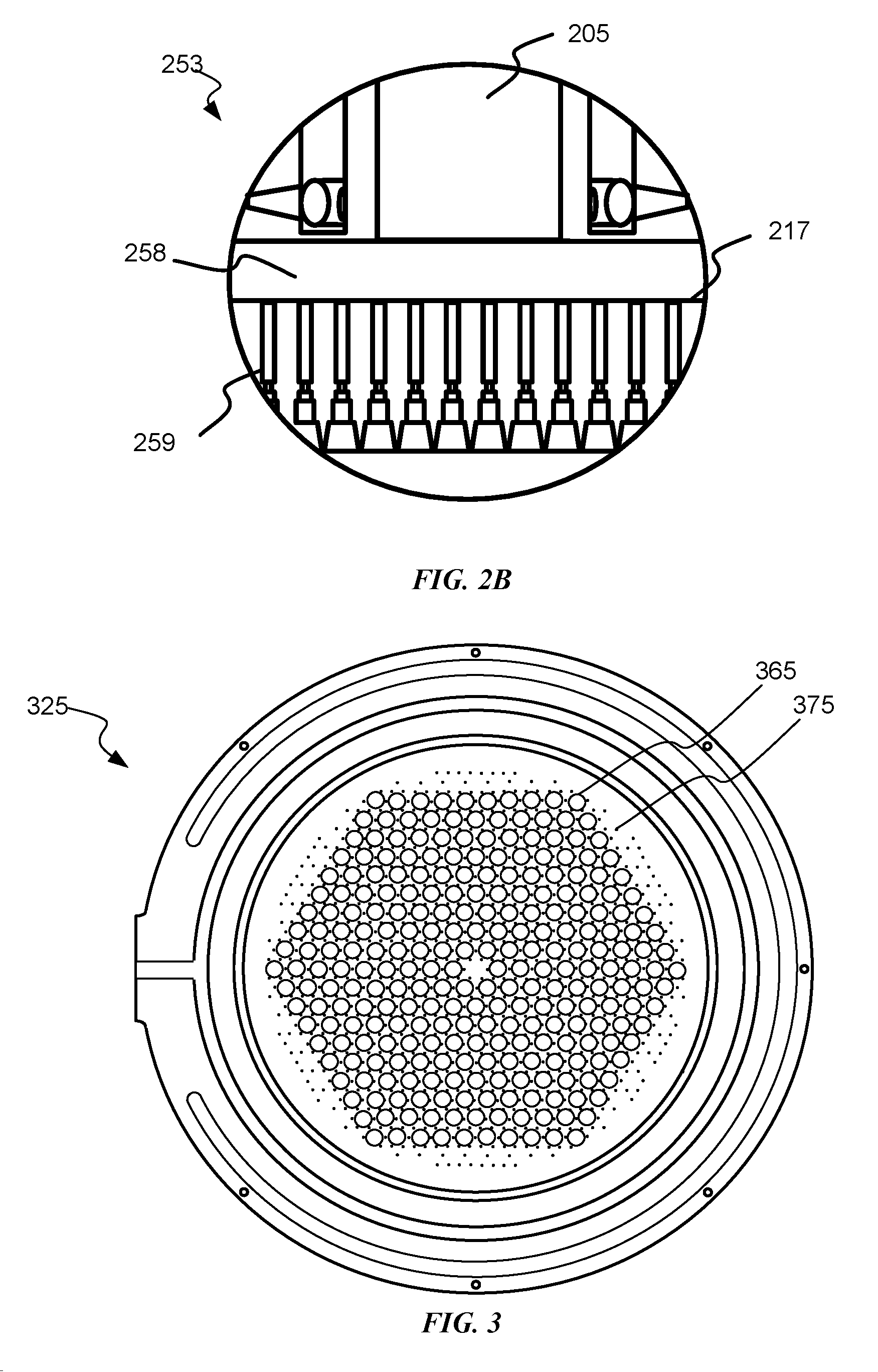
[0039] FIG. 2B shows a detailed view 253 of the features affecting the processing gas distribution through faceplate 217. As shown in FIGS. 2A and 2B, faceplate 217, cooling plate 203, and gas inlet assembly 205 intersect to define a gas supply region 258 into which process gases may be delivered from gas inlet 205. The gases may fill the gas supply region 258 and flow to first plasma region 215 through apertures 259 in faceplate 217. The apertures 259 may be configured to direct flow in a substantially unidirectional manner such that process gases may flow into processing region 233, but may be partially or fully prevented from backflow into the gas supply region 258 after traversing the faceplate 217.
[0040] The gas distribution assemblies such as showerhead 225 for use in the processing chamber section 200 may be referred to as dual channel showerheads (DCSH) and are additionally detailed in the embodiments described in FIG. 3. The dual channel showerhead may provide for etching processes that allow for separation of etchants outside of the processing region 233 to provide limited interaction with chamber components and each other prior to being delivered into the processing region.
[0041] The showerhead 225 may comprise an upper plate 214 and a lower plate 216. The plates may be coupled with one another to define a volume 218 between the plates. The coupling of the plates may be so as to provide first fluid channels 219 through the upper and lower plates, and second fluid channels 221 through the lower plate 216. The formed channels may be configured to provide fluid access from the volume 218 through the lower plate 216 via second fluid channels 221 alone, and the first fluid channels 219 may be fluidly isolated from the volume 218 between the plates and the second fluid channels 221. The volume 218 may be fluidly accessible through a side of the gas distribution assembly 225.
[0042] FIG. 3 is a bottom view of a showerhead 325 for use with a processing chamber according to embodiments. Showerhead 325 may correspond with the showerhead 225 shown in FIG. 2A. Through-holes 365, which show a view of first fluid channels 219, may have a plurality of shapes and configurations in order to control and affect the flow of precursors through the showerhead 225. Small holes 375, which show a view of second fluid channels 221, may be distributed substantially evenly over the surface of the showerhead, even amongst the through-holes 365, and may help to provide more even mixing of the precursors as they exit the showerhead than other configurations.
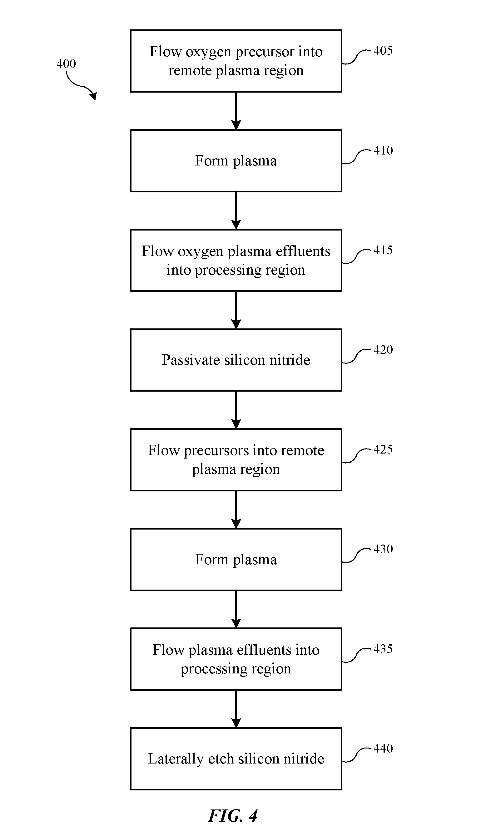
[0043] The chambers discussed previously may be used in performing exemplary methods including etching methods. Turning to FIG. 4 is shown exemplary operations in a method 400 according to embodiments of the present technology. Prior to the first operation of the method a substrate may be processed in one or more ways before being placed within a processing region of a chamber in which method 400 may be performed. For example, IPD layers may be formed on the substrate and then one or more memory holes or trenches may be formed through the stacked layers. The IPD layers may include any number of materials, and may include alternating layers of a placeholder material and a dielectric material. In embodiments the dielectric material may be or include silicon oxide, and the placeholder material may be or include silicon nitride. Although the remaining disclosure will discuss silicon nitride and silicon oxide, any other known materials used in these two layers may be substituted for one or more of the layers. Some or all of these operations may be performed in chambers or system tools as previously described, or may be performed in different chambers on the same system tool, which may include the chamber in which the operations of method 400 are performed.
[0044] The method 400 may include flowing an oxygen-containing precursor into a remote plasma region of a semiconductor processing chamber at operation 405. An exemplary chamber may be chamber 200 previously described, which may include one or both of the RPS unit 201 or first plasma region 215. Either or both of these regions may be the remote plasma region used in operation 405. A plasma may be generated within the remote plasma region at operation 410, which may generate plasma effluents of the oxygen-containing precursor. The plasma effluents may be flowed to a processing region of the chamber at operation 415. The oxygen-containing plasma effluents may interact with the substrate in the processing region, which may include a trench formed through stacked layers of material, and which may include alternating layers of silicon nitride and silicon oxide, for example, although other placeholder material and/or dielectric material may be used.
[0045] The oxygen-containing plasma effluents may have a greater interaction with silicon nitride materials than with the silicon oxide materials. Throughout the trench, the oxygen radicals may interact with the exposed surfaces of the silicon nitride, which may passivate the silicon nitride surface at operation 420, and may implant oxygen species at a surface of the silicon nitride. This may create a facial region of the exposed silicon nitride that includes Si--O--N structures, which may be beneficial to slow the etching process. Because the bonding of silicon nitride may be relatively strong, the passivation layer may be characterized by a thickness less than 5 nm in embodiments, and may be less than or about 4 nm, less than or about 3 nm, less than or about 2 nm, less than or about 1 nm, or may be down to about a monolayer of material.
[0046] After the passivation has been performed, a fluorine-containing precursor may be flowed into a remote plasma region at operation 425. Again, one or both of the RPS unit 201 or first plasma region 215 may be used as the remote plasma region into which the fluorine-containing precursor may be flowed. The oxygen-containing precursor may continue to be flowed into the remote plasma region in embodiments, and the flow may be maintained during operation 425. A plasma may be formed at operation 430 to produce fluorine-containing plasma effluents and oxygen-containing plasma effluents. In some embodiments, the plasma is maintained from the oxygen-containing precursor, and the fluorine-containing precursor is added to the flow to generate the additional plasma effluents, and an additional plasma may not be formed in some embodiments. The plasma effluents may be flowed into the process region and may contact the substrate at operation 435. The passivation layer may reduce or limit the etching operation, or essentially create an incubation period that is greater than the time for the plasma effluents to diffuse through the structure. This may allow the etching to be performed substantially simultaneously or essentially simultaneously throughout the structure. The passivation layer may be removed by the etching as well, which may expose the underlying silicon nitride at each level of the structure.
[0047] The plasma effluents may then laterally etch the layers of silicon nitride at operation 440. The lateral etching may be performed through the trench, such as a memory hole, and may occur from sidewalls within the trench along an exposed portion of each layer of silicon nitride, including along the passivated surfaces of the silicon nitride. In some embodiments, the lateral etching may be selectively performed on the silicon nitride layers, and may substantially maintain the intervening layers of silicon oxide or other dielectric material. Method 400 may laterally etch the silicon nitride less than 10 nm from the sidewalls of the trench in exemplary operations before the lateral etching operation ends, while in other embodiments a greater amount of etching is performed. For example, the silicon nitride may be maintained at an interior region, such as to act as a barrier layer, for example. The thickness of the remaining silicon nitride may be less than or about 20 nm in embodiments, and may be less than or about 18 nm, less than or about 16 nm, less than or about 15 nm, less than or about 14 nm, less than or about 13 nm, less than or about 12 nm, less than or about 11 nm, less than or about 10 nm, less than or about 9 nm, less than or about 8 nm, less than or about 7 nm, less than or about 6 nm, less than or about 5 nm, less than or about 4 nm, less than or about 3 nm, less than or about 2 nm, or less than or about 1 nm in embodiments.
[0048] Because the layer is reduced substantially in embodiments, the method may be performed to ensure a uniformity between the remaining layers at each level. During embodiments in which the process is performed to reduce several nanometers of silicon nitride, the method may be performed in multiple cycles, which may prevent the silicon oxide from being etched to maintain high selectivity. However, because the passivation layer is consumed, the entire process may be repeated in a number of cycles. The number of cycles performed may be based in part on the amount of silicon nitride to be removed. An additional benefit of the technology, however, is that to repeat the cycle, method 400 may be restarted in some embodiments by simply halting the flow of the fluorine-containing precursor. This may allow an additional passivation layer to be created prior to initiating flow of the fluorine-containing precursor once again.
[0049] Precursors used in the method may include a fluorine-containing precursor as well as an oxygen-containing precursor. An exemplary fluorine-containing precursor may be nitrogen trifluoride (NF.sub.3), which may be flowed into the remote plasma region, which may be separate from, but fluidly coupled with, the processing region. Other sources of fluorine may be used in conjunction with or as replacements for the nitrogen trifluoride. In general, a fluorine-containing precursor may be flowed into the remote plasma region and the fluorine-containing precursor may include at least one precursor selected from the group of atomic fluorine, diatomic fluorine, nitrogen trifluoride, carbon tetrafluoride, hydrogen fluoride, xenon difluoride, and various other fluorine-containing precursors used or useful in semiconductor processing. The oxygen-containing precursor may include a variety of fluids, and may include one or more of atomic oxygen, molecular oxygen, N.sub.2O, NO, NO.sub.2, ozone, or other oxygen-containing precursors that may be used or useful in semiconductor processes. The precursors may also include any number of carrier gases, which may include nitrogen, helium, argon, or other noble, inert, or useful precursors. The carrier gases may be used to dilute the precursors, which may further reduce etching rates to allow adequate diffusion through the trench.
[0050] In some embodiments, method 400 may involve tuning the oxygen to fluorine ratio of the precursors in embodiments. Although the passivation layer may provide sufficient protection to allow complete diffusion to occur prior to etching, in some embodiments, the amount of fluorine delivered may also be reduced. For example, a ratio of oxygen to fluorine precursors may include a flow rate ratio that is greater than or about 20:1 in embodiments. By increasing the oxygen flow rate and limiting the fluorine inclusion, oxidation may occur on the exposed regions of silicon nitride prior to the initiation of etching. Accordingly, the oxidation layer may operate similar to a barrier layer through which the fluorine containing etchant may diffuse. The time to diffuse through the oxidation portion of silicon nitride may be greater than the time to diffuse the precursors down through the memory hole or trench. In this way, an oxidation layer may be further produced during the etching operation in addition to the passivation layer prior to the etching, and may be formed along each exposed region of silicon nitride prior to etching of the regions of silicon nitride. The etchant may then be uniformly distributed through the trench and oxidation regions allowing a substantially similar amount of etching to occur on each exposed region of silicon nitride. Similarly, by limiting the amount of fluorine in the mixture, the amount of material etched from each exposed region of silicon nitride may be controlled.
[0051] In exemplary methods, such as method 400, the ratio of oxygen-containing precursor to fluorine-containing precursor may relate to the thickness of silicon nitride to be removed. For example, in methods in which more silicon nitride may be removed, additional fluorine-containing precursor may be included in the precursor mixture, or the time of the operations may be increased. To provide a lateral etch less than about 10 nm on each exposed region of silicon oxide within the trench, the ratio of oxygen-containing precursor to fluorine-containing precursor may be greater than or about 25:1, or may be greater than or about 30:1, greater than or about 35:1, greater than or about 40:1, greater than or about 45:1, greater than or about 50:1, greater than or about 55:1, greater than or about 60:1, greater than or about 65:1, greater than or about 70:1, greater than or about 75:1, greater than or about 80:1, or higher, as well as any smaller range included within any of the stated ranges. For example, a flow rate of greater than or about 60:1, may allow the formation of a fluorinated oxide region on each exposed region of silicon nitride. The flow rate ratio may be maintained higher than 40:1 in embodiments to reduce the amount of silicon nitride etched throughout the length of the trench. When the amount of fluorine is increased in the mixture, regions of silicon nitride at or near the top of the trench may begin to etch before the oxidation portion has formed. This may then still produce a profile within the trench, such as a V-profile of silicon nitride layers from the top to the bottom of the trench. However, by forming a passivation layer as previously discussed, etching along the top of the trench may be limited or prevented to maintain uniform etching through the trench.
[0052] The V-profile may be unavoidable with conventional dry technologies because of the high aspect ratios of trenches or memory holes in which the lateral etching may be performed. The diameter or width of exemplary trenches may be a few tens or nanometers or less, while the height of the trenches may be on the order or a few microns or more. This may produce aspect ratios or height to width ratios of greater than 20:1, greater than 50:1, greater than 75:1, greater than 100:1, or even greater. Accordingly, in embodiments over 25 layers, over 50 layers, over 75 layers, or over one hundred layers of alternating placeholder material and dielectric material may be formed and processed within each trench.
[0053] Because of the greater lengths a dry or gaseous etchant may travel, the top regions of the trench may be exposed to significant amounts of etchant before the etchant has even reached the bottom of the trench. In this way, the silicon nitride located at upper regions of the trench may be etched more than portions at the bottom of the trench. Although a wet etch technique may more uniformly etch the layers of silicon nitride, it may be incapable of etching less than 10 or more nanometers because of the properties and residence time of the etchant. Accordingly, no conventional technologies may be capable of finely etching an amount of material from each silicon nitride layer, such as only a few nanometers, as well as produce a flat or substantially similar profile of etched silicon nitride throughout the trench, unlike the present technology. The present technology, however, may compensate for the greater diffusion pathway by creating a passivation layer to limit etching during diffusion, or by limiting the etchant in any of the ways discussed to allow a more uniform etching process to occur.
[0054] In some embodiments, the oxygen-containing precursor may be flowed into a first remote plasma region, such as the RPS unit 201. The RPS unit may be operated at a higher plasma power, such as from one hundred Watts or less up to about 20 kW or more. Operating the RPS at higher power may allow complete dissociation of the oxygen-containing precursor in some embodiments, which may facilitate the passivation operation. In some embodiments the fluorine-containing precursor may be flowed into a second remote plasma region, such as region 215, where a capacitively-coupled plasma may be formed. In region 215, the plasma power may be maintained at a lower amount, such as from about 25 W to about 500 W. This may reduce the dissociation of the fluorine-containing precursor, which may reduce the aggressiveness of the etching operation.
[0055] The fluorine-containing precursor may be flowed to bypass the RPS unit when flow of the fluorine-containing precursor is initiated. Accordingly, in some embodiments the capacitively-coupled plasma may be initiated only when the fluorine-containing precursor is flowed into the chamber, while the RPS unit is operated at all times during the constant flow of the oxygen-containing precursor. Additionally, because flow of the oxygen-containing precursor may pass through region 215, plasma may be formed in this region at all times as well, and the cycling feature may be limited to the on/off flow of the fluorine-containing precursor to differentiate between the passivation operations and the etching operations. In other embodiments different combinations of flowing the precursors between plasma regions may be performed, such as both precursors may be flowed into region 215, or all dissociation may occur in RPS unit 201, or the precursors may be enhanced in both RPS unit 201 as well as region 215 in embodiments.
[0056] The passivating operation and the etching operation may each be performed for a period of time. For example, the passivation operation may be performed to produce an amount of passivation on each exposed layer of silicon nitride from top to bottom within the structure. Because of the aspect ratio of the structure, the passivation may be performed for a first period of time to ensure the process creates a uniform amount of passivation. In some embodiments, the passivation may be performed for greater than or about 30 seconds, and may be performed for greater than or about 45 seconds, greater than or about 1 minute, greater than or about 1.25 minutes, greater than or about 1.5 minutes, greater than or about 1.75 minutes, greater than or about 2 minutes, greater than or about 2.25 minutes, greater than or about 2.5 minutes, greater than or about 2.75 minutes, greater than or about 3 minutes, or more. The time may be dependent on the length of the trench or memory hole, chamber conditions, plasma power, or other variables, and thus while in some embodiments the passivation operation may be performed for less than or about 2 minutes, in some embodiments it may be performed for greater than or about 5 minutes, for example.
[0057] The etching may be performed for a second period of time, and in some embodiments the second period of time may be greater than the first period of time. In some embodiments the etching may be performed for greater than or about 30 seconds, greater than or about 1 minute, greater than or about 2 minutes, greater than or about 3 minutes, greater than or about 4 minutes, greater than or about 5 minutes, greater than or about 6 minutes, greater than or about 7 minutes, greater than or about 8 minutes, greater than or about 9 minutes, greater than or about 10 minutes, or more. However, the longer the etching is performed, the likelihood of etching silicon oxide increases, which may reduce selectivity, or may reduce an amount of oxide within the structure, which may lead to crosstalk between formed cells. Accordingly, the etching operation may be performed for less than 10 minutes in some embodiments, and may be performed for less than or about 8 minutes, less than or about 7 minutes, less than or about 6 minutes, less than or about 5 minutes, or less.
[0058] Process conditions may also impact the operations performed in method 400 as well as other etching methods according to the present technology. Each of the operations of method 400 may be performed during a constant temperature in embodiments, while in some embodiments the temperature may be adjusted during different operations. For example, the substrate, pedestal, or chamber temperature during the passivating operation 420 or the lateral etching operation 440 may be maintained between about -100.degree. C. and about 100.degree. C. in embodiments. The temperature may also be maintained below or about 80.degree. C., below or about 60.degree. C., below or about 40.degree. C., below or about 20.degree. C., below or about 0.degree. C., below or about -20.degree. C., below or about -40.degree. C., or lower. Temperature may affect the etching process itself, and higher temperature may produce higher etch rates, increased etching, or other effects. However, although lower temperatures may slow the etching operation and allow the oxidation of portions of silicon nitride prior to the etching, lower temperatures may detrimentally affect the passivation operation. Thus, in some embodiments, maintaining a temperature between about 0.degree. C. and about 50.degree. C. may provide more uniform etching amounts of silicon nitride at the top of the trench and at the bottom of the trench. As temperature increases, the etching operations may additionally begin to affect the dielectric regions, and may cause slight rounding of exposed corners or regions of the dielectric material, such as silicon oxide.
[0059] The pressure within the chamber may also affect the operations performed, and in embodiments the chamber pressure may be maintained below about 10 Torr, below about 5 Torr, or below about 1 Torr. In embodiments a pressure below or about 1 Torr may allow the precursors or plasma effluents to more easily flow into the trenches or memory holes. However, when the pressure is reduced below about 0.5 Torr, a remote plasma may be affected, and may have reduced stability or may become unstable. As mentioned previously, the remote plasma may include an RPS unit, and may also be a region or portion of the chamber physically partitioned from the processing region of the chamber to limit or eliminate plasma at the wafer level. In some embodiments in which an RPS unit is utilized, a choke may be utilized to maintain a higher pressure within the RPS unit for plasma stability with a lower pressure within a chamber for improved in-trench flow of precursors or plasma effluents. Accordingly, a turbomolecular pump may be utilized in the chamber allowing a chamber pressure down to a few milliTorr, while the RPS is maintained above or about 0.6 Torr.
[0060] Pressure may also affect the mean free path of a particle before contacting another particle, and affecting the operation being performed. Higher pressures may reduce the mean free path, which may cause further etchant contact at upper portions of the trench, while lower pressures may increase the mean free path and facilitate diffusion. Accordingly, in some embodiments the etching operation 440 may be performed at pressures below or about 1 Torr. However, particle contact may facilitate the passivation operation 420, creating more uniform passivation through the structure. Hence, in some embodiments the passivation operation may be performed at higher pressures than the etching operations, and for example, the passivation operation may be performed at pressures greater than or about 1 Torr. Modulating pressure during and between cycles may increase queue times, however, and thus in some embodiments pressure may be substantially maintained between the passivation operations and the etching operations.
[0061] By performing the operations according to the present technology, the etching power may be reduced relative to the diffusion power of the etchant materials, or may be delayed due to formation of the passivation layer, which may allow a more uniform, substantially uniform, or essentially uniform etch to be performed at each silicon nitride region exposed within the trench or memory hole. In embodiments, a silicon nitride region at or near the top of the trench or memory hole, such as within 2 layers from the top, within 4 layers, within 6 layers, within 8 layers, within 10 layers, or more, may have an amount of material etched measured from the sidewall that is similar to a silicon nitride layer or region at or near the bottom of the trench of memory hole, such as within 2 layers from the bottom, within 4 layers, within 6 layers, within 8 layers, within 10 layers, or more.
[0062] The two layers being compared may be separated by at least 1 layer, at least 5 layers, at least 11 layers, at least 21 layers, at least 51 layers or more depending on the overall number of stacked layers within the structure through which the trench or memory hole has been etched. The lateral etch of the two layers being compared may differ by less than or about 30%, in terms of the upper layer being etched no more than 30% more than the lower layer. Additionally, the present technology may perform a lateral etch of the two layers so a difference between the amount of silicon nitride etched between the two layers is less than or about 25%, less than or about 20%, less than or about 15%, less than or about 10%, less than or about 5%, less than or about 1%, or zero difference in which case both regions of silicon oxide are etched to an equal depth or distance from a sidewall of the trench. Similarly, the amount of silicon nitride maintained at each layer within the trench may be substantially similar to layers at any other location within the structure, and the amount of material remaining may differ between any two layers by less than or about 5 nm, and may differ by less than or about 4 nm, less than or about 3 nm, less than or about 2 nm, less than or about 1.5 nm, less than or about 1 nm, less than or about 0.5 nm, or less.
[0063] FIG. 5 shows exemplary operations in a method 500 according to embodiments of the present technology. Method 500 may include some or all of the operations of method 400 explained above, and may include any of the components or conditions discussed there. Method 500 may differ from method 400 by depositing a sacrificial layer over the silicon nitride material instead of forming a passivation layer. For example, method 500 may include delivering deposition precursors to the substrate at operation 505. The deposition precursors may include a silicon-containing precursor, such as silane, for example, and may include an oxygen or nitrogen-containing precursor. One or both precursors may be enhanced prior to delivery into the processing region of the chamber, where a layer of material may be formed over the silicon nitride material at operation 510. The sacrificial layer may be silicon oxide in some embodiments, although in other embodiments any other material that can be subsequently etched may be used. The sacrificial layer may be produced along all layers of nitride in the structure, while in other embodiments the sacrificial layer may be produced along a gradient where the greatest deposition occurs on layers of nitride near the top of the trench and the least amount of deposition, which may include no deposition in some embodiments, may occur at the lower or lowest layers of nitride within the trench.
[0064] Method 500 may include flowing a fluorine-containing precursor and an oxygen-containing precursor into a remote plasma region of a semiconductor processing chamber at operation 515. In some embodiments, one or more of the precursors may be flowed into the remote plasma region, while one or more other precursors may bypass the remote plasma region, and may contact the plasma effluents subsequent plasma processing. The remote plasma region may include one or more remote plasma regions including a partitioned region of the processing chamber, or a remote section fluidly coupled with the processing chamber. Accordingly, some precursors may only be excited by contact with other radical components. In other embodiments all precursors may be flowed through the remote plasma region.
[0065] A plasma may be formed of these precursors at operation 520. The plasma may generate plasma effluents of the fluorine-containing and oxygen-containing precursors. The primary plasma effluents may be flowed into a processing region of the processing chamber where a substrate is housed at operation 525. The substrate may include a trench, such as a memory hole, formed through stacked layers including alternative layers of silicon nitride and silicon oxide such as previously described, and may include the sacrificial material over some portions of the silicon nitride. At operation 530, the silicon nitride materials may be etched. The sacrificial material may be removed before exposing the underlying nitride, which may allow the etchant precursors to diffuse fully while the sacrificial layer is being removed at upper regions of the trench. This may facilitate uniform etching of the silicon nitride materials laterally through the structure. The etching may be performed at any of the conditions previously described, and may produce similar results as described above.
[0066] As discussed previously, the operation may produce substantially uniform etching on the layers of silicon oxide from the top of the trench to the bottom of the trench, also called top to bottom loading. This may allow a layer of silicon nitride at an upper region of the trench and a layer of silicon nitride at a lower region of the trench to differ in lateral etch amounts by less than about 20% or by any of the differences and/or depths as previously discussed. The uniformity may occur in part to the conditions in which the operations are performed, as well as due to formation of the sacrificial layer along surfaces of the silicon nitride layers.
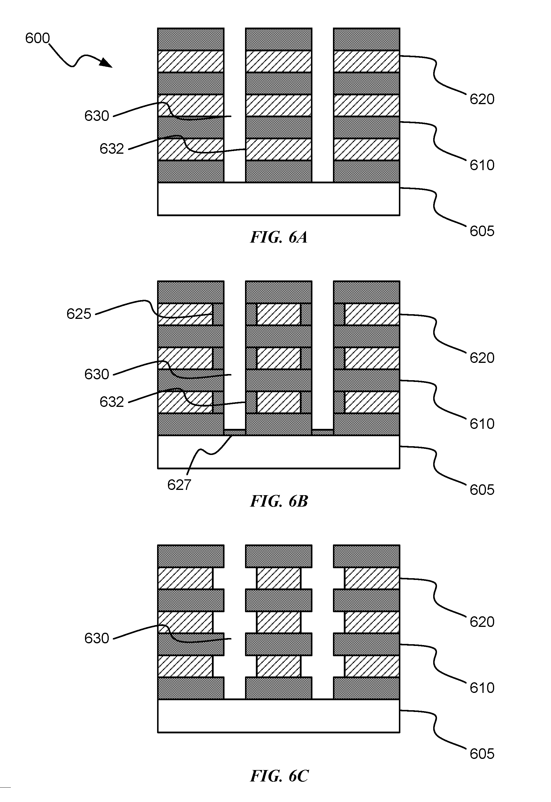
[0067] Turning to FIGS. 6A-6C are shown cross-sectional views of structure 600 being processed according to embodiments of the present technology. As illustrated in FIG. 6A substrate 605 may have a plurality of stacked layers overlying the substrate, which may be silicon, silicon germanium, or other substrate materials. The layers may include IPD layers including dielectric material 610, which may be silicon oxide, in alternating layers with placeholder material 620, which may be silicon nitride. Placeholder material 620 may be or include material that will be removed to produce individual memory cells in subsequent operations. Although illustrated with only 7 layers of material, exemplary structures may include any of the numbers of layers previously discussed. Trenches 630, which may be memory holes, may be defined through the stacked structure to the level of substrate 605. Trenches 630 may be defined by sidewalls 632 that may be composed of the alternating layers of dielectric material 610 and placeholder material 620.
[0068] In FIG. 6B may be illustrated a structure after methods according to the present technology have been performed, such as discussed with respect to FIGS. 4-5 above. A portion of each exposed surface of silicon nitride layers 620 may be passivated to produce oxidized regions 625, or which may be rendered less reactive by the passivation. The oxidized regions may be an oxidized region of silicon nitride, which may include oxygen atoms within the nitride structure. Although not illustrated, oxidation regions 625 may be partially recessed from the sidewalls 632 of the trench 630, such as to a distance of greater than, about, or less than about 3 nm, 2 nm, 1 nm, or less as previously described. The oxidation may not affect dielectric layers 610, as these layers may already be oxide, for example. However, substrate 605 may include a thin layer of oxidation 627, which may be less than or equal to the depth of oxidation of the silicon nitride layers 620. In other embodiments the substrate may have minimal or substantially no oxidation.
[0069] FIG. 6C illustrates a structure after further methods or operations according to the present technology have been performed, such as discussed with respect to FIGS. 4-5 above. An etching operation may be performed to remove the passivated portions of silicon nitride layers 620 as well as a portion of the underlying silicon nitride. The etching may remove the materials to form a recessed region of silicon nitride from the trenches 630 and the silicon oxide layers 610. The layers may be recessed to any extent depending on the amount of material to be removed, and the number of cycles to be performed, and may be removed within any of the ranges discussed elsewhere in this disclosure. Substrate 605 may show minimal etching at the bottom of trenches 630, and may be reduced by an amount less than or about 5 nm, and may be reduced by an amount less than or about 3 nm, less than or about 2 nm, less than or about 1 nm, or may be substantially maintained during the lateral etching operations of silicon nitride.
[0070] In the preceding description, for the purposes of explanation, numerous details have been set forth in order to provide an understanding of various embodiments of the present technology. It will be apparent to one skilled in the art, however, that certain embodiments may be practiced without some of these details, or with additional details.
[0071] Having disclosed several embodiments, it will be recognized by those of skill in the art that various modifications, alternative constructions, and equivalents may be used without departing from the spirit of the embodiments. Additionally, a number of well-known processes and elements have not been described in order to avoid unnecessarily obscuring the present technology. Accordingly, the above description should not be taken as limiting the scope of the technology. Additionally, methods or processes may be described as sequential or in steps, but it is to be understood that the operations may be performed concurrently, or in different orders than listed.
[0072] Where a range of values is provided, it is understood that each intervening value, to the smallest fraction of the unit of the lower limit, unless the context clearly dictates otherwise, between the upper and lower limits of that range is also specifically disclosed. Any narrower range between any stated values or unstated intervening values in a stated range and any other stated or intervening value in that stated range is encompassed. The upper and lower limits of those smaller ranges may independently be included or excluded in the range, and each range where either, neither, or both limits are included in the smaller ranges is also encompassed within the technology, subject to any specifically excluded limit in the stated range. Where the stated range includes one or both of the limits, ranges excluding either or both of those included limits are also included.
[0073] As used herein and in the appended claims, the singular forms "a", "an", and "the" include plural references unless the context clearly dictates otherwise. Thus, for example, reference to "a precursor" includes a plurality of such precursors, and reference to "the layer" includes reference to one or more layers and equivalents thereof known to those skilled in the art, and so forth.
[0074] Also, the words "comprise(s)", "comprising", "contain(s)", "containing", "include(s)", and "including", when used in this specification and in the following claims, are intended to specify the presence of stated features, integers, components, or operations, but they do not preclude the presence or addition of one or more other features, integers, components, operations, acts, or groups.
* * * * *
D00000
D00001
D00002
D00003
D00004
D00005
D00006
XML
uspto.report is an independent third-party trademark research tool that is not affiliated, endorsed, or sponsored by the United States Patent and Trademark Office (USPTO) or any other governmental organization. The information provided by uspto.report is based on publicly available data at the time of writing and is intended for informational purposes only.
While we strive to provide accurate and up-to-date information, we do not guarantee the accuracy, completeness, reliability, or suitability of the information displayed on this site. The use of this site is at your own risk. Any reliance you place on such information is therefore strictly at your own risk.
All official trademark data, including owner information, should be verified by visiting the official USPTO website at www.uspto.gov. This site is not intended to replace professional legal advice and should not be used as a substitute for consulting with a legal professional who is knowledgeable about trademark law.