High Resistivity Silicon-on-insulator Substrate Comprising A Charge Trapping Layer Formed On A Substrate With A Rough Surface
Peidous; Igor ; et al.
U.S. patent application number 16/077142 was filed with the patent office on 2019-01-24 for high resistivity silicon-on-insulator substrate comprising a charge trapping layer formed on a substrate with a rough surface. The applicant listed for this patent is Igor PEIDOUS, SUNEDISON SEMCONDUCTOR LIMITED. Invention is credited to Andrew M. Jones, Srikanth Kommu, Jeffrey L. Libbert, Igor Peidous, Gang Wang.
| Application Number | 20190027397 16/077142 |
| Document ID | / |
| Family ID | 58046764 |
| Filed Date | 2019-01-24 |


| United States Patent Application | 20190027397 |
| Kind Code | A1 |
| Peidous; Igor ; et al. | January 24, 2019 |
HIGH RESISTIVITY SILICON-ON-INSULATOR SUBSTRATE COMPRISING A CHARGE TRAPPING LAYER FORMED ON A SUBSTRATE WITH A ROUGH SURFACE
Abstract
A multilayer composite structure and a method of preparing a multilayer composite structure are provided. The multilayer composite structure comprises a semiconductor handle substrate having a minimum bulk region resistivity of at least about 500 ohm-cm and the front surface of the single crystal semiconductor handle substrate has a surface roughness of at least about 0.1 micrometers as measured according to the root mean square method over a surface area of at least 30 micrometers by 30 micrometers. The composite structure further comprises a charge trapping layer in contact with the front surface, the charge trapping layer comprising poly crystalline silicon, the poly crystalline silicon comprising grains having a plurality of crystal orientations; a dielectric layer in contact with the charge trapping layer; and a single crystal semiconductor device layer in contact with the dielectric layer.
| Inventors: | Peidous; Igor; (Eaton, OH) ; Jones; Andrew M.; (Wildwood, MO) ; Kommu; Srikanth; (St. Charles, MO) ; Wang; Gang; (Grover, MO) ; Libbert; Jeffrey L.; (O'Fallon, MO) | ||||||||||
| Applicant: |
|
||||||||||
|---|---|---|---|---|---|---|---|---|---|---|---|
| Family ID: | 58046764 | ||||||||||
| Appl. No.: | 16/077142 | ||||||||||
| Filed: | January 31, 2017 | ||||||||||
| PCT Filed: | January 31, 2017 | ||||||||||
| PCT NO: | PCT/US2017/015813 | ||||||||||
| 371 Date: | August 10, 2018 |
Related U.S. Patent Documents
| Application Number | Filing Date | Patent Number | ||
|---|---|---|---|---|
| 62297253 | Feb 19, 2016 | |||
| Current U.S. Class: | 1/1 |
| Current CPC Class: | H01L 21/28176 20130101; H01L 21/02529 20130101; H01L 21/0245 20130101; H01L 21/76254 20130101; H01L 21/0262 20130101; H01L 21/02532 20130101 |
| International Class: | H01L 21/762 20060101 H01L021/762; H01L 21/28 20060101 H01L021/28; H01L 21/02 20060101 H01L021/02 |
Claims
1. A multilayer structure comprising: a single crystal semiconductor handle substrate comprising two major, generally parallel surfaces, one of which is a roughened front surface of the single crystal semiconductor handle substrate and the other of which is a back surface of the single crystal semiconductor handle substrate, a circumferential edge joining the roughened front surface and the back surface of the single crystal semiconductor handle substrate, a central plane between the roughened front surface and the back surface of the single crystal semiconductor handle substrate, and a bulk region between the front and back surfaces of the single crystal semiconductor handle substrate, wherein the single crystal semiconductor handle substrate has a minimum bulk region resistivity of at least about 500 ohm-cm and the roughened front surface of the single crystal semiconductor handle substrate has a surface roughness of at least about 0.01 micrometers as measured according to the root mean square method over a surface area of at least 30 micrometers by 30 micrometers; a charge trapping layer in contact with the roughened front surface single crystal semiconductor handle substrate, the charge trapping layer comprising polycrystalline silicon, the polycrystalline silicon comprising grains having a plurality of random crystal orientations and having a grain size between about 10 nanometers and about 3 micrometers; a dielectric layer in contact with the charge trapping layer; and a single crystal semiconductor device layer in contact with the dielectric layer.
2. The multilayer structure of claim 1 wherein the single crystal semiconductor handle substrate comprises single crystal silicon.
3. The multilayer structure of claim 1 wherein the single crystal semiconductor handle substrate comprises a single crystal silicon wafer sliced from a single crystal silicon ingot grown by the Czochralski method or the float zone method.
4. (canceled)
5. The multilayer structure of claim 1 wherein the single crystal semiconductor handle substrate has a bulk resistivity between about 1000 Ohm-cm and about 100,000 Ohm-cm.
6. The multilayer structure of claim 1 wherein the single crystal semiconductor handle substrate has a bulk resistivity between about 1000 ohm cm and about 10,000 Ohm-cm.
7. The multilayer structure of claim 1 wherein the single crystal semiconductor handle substrate has a bulk resistivity between about 2000 Ohm cm and about 10,000 Ohm-cm.
8. The multilayer structure of claim 1 wherein the single crystal semiconductor handle substrate has a bulk resistivity between about 3000 Ohm-cm and about 10,000 Ohm-cm.
9. The multilayer structure of claim 1 wherein the single crystal semiconductor handle substrate has a bulk resistivity between about 3000 Ohm cm and about 5,000 Ohm-cm.
10. The multilayer structure of claim 1 wherein the surface roughness of the roughened front surface of the single crystal semiconductor handle substrate is between about 0.1 micrometer and about 1 micrometer as measured according to the root mean square method over a surface area of at least 30 micrometers by 30 micrometers.
11. The multilayer structure of claim 1 wherein the plurality of crystal orientations of the polycrystalline silicon comprising grains comprise at least two orientations selected from the group consisting of (111), (100), and (110).
13. The multilayer structure of claim 1 wherein the dielectric layer comprises a material selected from the group consisting of silicon dioxide, silicon nitride, hafnium oxide, titanium oxide, zirconium oxide, lanthanum oxide, barium oxide, and a combination thereof.
14. The multilayer structure of claim 1 wherein the dielectric layer comprises a buried oxide layer having a thickness of at least about 10 nanometer.
15. The multilayer structure of claim 1 wherein the single crystal semiconductor device layer comprises single crystal silicon.
16. A method of forming a multilayer structure, the method comprising: implanting ions selected from the group consisting of He.sup.+, H.sup.+, H.sub.2.sup.+, and any combination thereof through a front surface of a single crystal semiconductor handle substrate to thereby prepare an implant layer in a front surface region of the single crystal semiconductor handle substrate, wherein the single crystal semiconductor handle substrate comprises two major, generally parallel surfaces, one of which is the front surface of the single crystal semiconductor handle substrate and the other of which is a back surface of the single crystal semiconductor handle substrate, a circumferential edge joining the front and back surfaces of the single crystal semiconductor handle substrate, a central plane between the front surface and the back surface of the single crystal semiconductor handle substrate, a front surface region having a depth, D, as measured from the front surface and toward the central plane, and a bulk region between the front and back surfaces of the single crystal semiconductor handle substrate, wherein the single crystal semiconductor handle substrate has a minimum bulk region resistivity of at least about 500 ohm-cm; heating the ion-implanted single crystal semiconductor handle substrate at a temperature and a duration sufficient to out-diffuse the implanted species and thereby form an agglomeration layer in the front surface region of the single crystal semiconductor handle substrate, the agglomeration layer forming at a depth, D1, as measured from the front surface and toward the central plane; mechanically cleaving the single crystal semiconductor handle substrate at the agglomeration layer to thereby expose a roughened front surface of the single crystal semiconductor handle substrate, wherein the roughened front surface has a surface roughness of at least about 0.01 micrometers as measured according to the root mean square method over a surface area of at least 30 micrometers by 30 micrometers; depositing a charge trapping layer on the roughened front surface, the charge trapping layer comprising polycrystalline silicon, the polycrystalline silicon comprising grains having a plurality of crystal orientations; and bonding a dielectric layer on a front surface of a single crystal semiconductor donor substrate to the charge trapping layer to thereby form a bonded structure, wherein the single crystal semiconductor donor substrate comprises two major, generally parallel surfaces, one of which is the front surface of the semiconductor donor substrate and the other of which is a back surface of the semiconductor donor substrate, a circumferential edge joining the front and back surfaces of the semiconductor donor substrate, and a central plane between the front and back surfaces of the semiconductor donor substrate, and further wherein the front surface of the semiconductor donor substrate comprises the dielectric layer.
17. The method of claim 15 wherein the single crystal semiconductor handle substrate comprises single crystal silicon.
18. The method of claim 15 wherein the single crystal semiconductor handle substrate comprises a single crystal silicon wafer sliced from a single crystal silicon ingot grown by the Czochralski method or the float zone method.
19. (canceled)
20. The method of claim 15 wherein the single crystal semiconductor handle substrate has a bulk resistivity between about 1000 Ohm-cm and about 100,000 Ohm-cm.
21. The method of claim 15 wherein the single crystal semiconductor handle substrate has a bulk resistivity between about 1000 ohm cm and about 10,000 Ohm-cm.
22. The method of claim 15 wherein the single crystal semiconductor handle substrate has a bulk resistivity between about 2000 Ohm cm and about 10,000 Ohm-cm.
23. The method of claim 15 wherein the single crystal semiconductor handle substrate has a bulk resistivity between about 3000 Ohm-cm and about 10,000 Ohm-cm.
24. The method of claim 15 wherein the single crystal semiconductor handle substrate has a bulk resistivity between about 3000 Ohm cm and about 5,000 Ohm-cm.
25. The method of claim 15 wherein the surface roughness of the roughened front surface of the single crystal semiconductor handle substrate is between about 0.1 micrometer and about 1 micrometer.
26. The method of claim 15 wherein the plurality of crystal orientations of the polycrystalline silicon comprising grains comprise at least two orientations selected from the group consisting of (111), (100), and (110).
27. The method of claim 15 wherein the dielectric layer comprises a material selected from the group consisting of silicon dioxide, silicon nitride, hafnium oxide, titanium oxide, zirconium oxide, lanthanum oxide, barium oxide, and a combination thereof.
28. The method of claim 15 wherein the dielectric layer comprises a buried oxide layer having a thickness of at least about 10 nanometer.
29. The method of claim 15 further comprising heating the bonded structure at a temperature and for a duration sufficient to strengthen the bond between the dielectric layer of the single crystal semiconductor donor substrate and the charge trapping layer on the on the roughened front surface of the single crystal semiconductor handle substrate.
30. The method of claim 15 wherein the single crystal semiconductor donor substrate comprises an ion implanted damage layer.
31. The method of claim 30 further comprising mechanically cleaving the bonded structure at the ion implanted damage layer of the single crystal semiconductor donor substrate to thereby prepare a cleaved structure comprising the single crystal semiconductor handle substrate having a roughened front surface, the charge trapping layer in contact with the roughened front surface, the dielectric layer in contact with the charge trapping layer, and a single crystal semiconductor device layer.
32. The method of claim 30 wherein the charge trapping layer has a resistivity between about 1000 Ohm-cm and about 100,000 Ohm-cm.
33. The method of claim 30 wherein the charge trapping layer further comprises carbon at a concentration between about 1% on an atomic basis and about 10% on an atomic basis.
Description
CROSS REFERENCE TO RELATED APPLICATION(S)
[0001] This application claims the benefit of priority to U.S. provisional application Ser. No. 62/297,253, which was filed 19 Feb. 2016, the disclosure of which is hereby incorporated by reference as if set forth in its entirety.
FIELD OF THE INVENTION
[0002] The present invention generally relates to the field of semiconductor wafer manufacture. More specifically, the present invention relates to a method of preparing a handle substrate for use in the manufacture of a semiconductor-on-insulator (e.g., silicon-on-insulator) structure, and more particularly to a method for producing a charge trapping layer in the handle wafer of the semiconductor-on-insulator structure.
BACKGROUND OF THE INVENTION
[0003] Semiconductor wafers are generally prepared from a single crystal ingot (e.g., a silicon ingot) which is trimmed and ground to have one or more flats or notches for proper orientation of the wafer in subsequent procedures. The ingot is then sliced into individual wafers. While reference will be made herein to semiconductor wafers constructed from silicon, other materials may be used to prepare semiconductor wafers, such as germanium, silicon carbide, silicon germanium, gallium arsenide, and other alloys of Group III and Group V elements, such as gallium nitride or indium phosphide, or alloys of Group II and Group IV elements, such as cadmium sulfide or zinc oxide.
[0004] Semiconductor wafers (e.g., silicon wafers) may be utilized in the preparation of composite layer structures. A composite layer structure (e.g., a semiconductor-on-insulator, and more specifically, a silicon-on-insulator (SOI) structure) generally comprises a handle wafer or layer, a device layer, and an insulating (i.e., dielectric) film (typically an oxide layer) between the handle layer and the device layer. Generally, the device layer is between 0.01 and 20 micrometers thick, such as between 0.05 and 20 micrometers thick. In general, composite layer structures, such as silicon-on-insulator (SOI), silicon-on-sapphire (SOS), and silicon-on-quartz, are produced by placing two wafers in intimate contact, followed by a thermal treatment to strengthen the bond. The anneal may convert the terminal silanol groups to siloxane bonds between the two interfaces, thereby strengthening the bond.
[0005] After thermal anneal, the bonded structure undergoes further processing to remove a substantial portion of the donor wafer to achieve layer transfer. For example, wafer thinning techniques, e.g., etching or grinding, may be used, often referred to as back etch SOI (i.e., BESOI), wherein a silicon wafer is bound to the handle wafer and then slowly etched away until only a thin layer of silicon on the handle wafer remains. See, e.g., U.S. Pat. No. 5,189,500, the disclosure of which is incorporated herein by reference as if set forth in its entirety. This method is time-consuming and costly, wastes one of the substrates and generally does not have suitable thickness uniformity for layers thinner than a few microns.
[0006] Another common method of achieving layer transfer utilizes a hydrogen implant followed by thermally induced layer splitting. Particles (atoms or ionized atoms, e.g., hydrogen atoms or a combination of hydrogen and helium atoms) are implanted at a specified depth beneath the front surface of the donor wafer. The implanted particles form a cleave plane in the donor wafer at the specified depth at which they were implanted. The surface of the donor wafer is cleaned to remove organic compounds or other contaminants, such as boron compounds, deposited on the wafer during the implantation process.
[0007] The front surface of the donor wafer is then bonded to a handle wafer to form a bonded wafer through a hydrophilic bonding process. Prior to bonding, the donor wafer and/or handle wafer are activated by exposing the surfaces of the wafers to plasma containing, for example, oxygen or nitrogen. Exposure to the plasma modifies the structure of the surfaces in a process often referred to as surface activation, which activation process renders the surfaces of one or both of the donor water and handle wafer hydrophilic. The surfaces of the wafers can be additionally chemically activated by a wet treatment, such as an SC1 clean or hydrofluoric acid. The wet treatment and the plasma activation may occur in either order, or the wafers may be subjected to only one treatment. The wafers are then pressed together, and a bond is formed there between. This bond is relatively weak, due to van der Waal's forces, and must be strengthened before further processing can occur.
[0008] In some processes, the hydrophilic bond between the donor wafer and handle wafer (i.e., a bonded wafer) is strengthened by heating or annealing the bonded wafer pair. In some processes, wafer bonding may occur at low temperatures, such as between approximately 300.degree. C. and 500.degree. C. In some processes, wafer bonding may occur at high temperatures, such as between approximately 800.degree. C. and 1100.degree. C. The elevated temperatures cause the formation of covalent bonds between the adjoining surfaces of the donor wafer and the handle wafer, thus solidifying the bond between the donor wafer and the handle wafer. Concurrently with the heating or annealing of the bonded wafer, the particles earlier implanted in the donor wafer weaken the cleave plane.
[0009] A portion of the donor wafer is then separated (i.e., cleaved) along the cleave plane from the bonded wafer to form the SOI wafer. Cleaving may be carried out by placing the bonded wafer in a fixture in which mechanical force is applied perpendicular to the opposing sides of the bonded wafer in order to pull a portion of the donor wafer apart from the bonded wafer. According to some methods, suction cups are utilized to apply the mechanical force. The separation of the portion of the donor wafer is initiated by applying a mechanical wedge at the edge of the bonded wafer at the cleave plane in order to initiate propagation of a crack along the cleave plane. The mechanical force applied by the suction cups then pulls the portion of the donor wafer from the bonded wafer, thus forming an SOI wafer.
[0010] According to other methods, the bonded pair may instead be subjected to an elevated temperature over a period of time to separate the portion of the donor wafer from the bonded wafer. Exposure to the elevated temperature causes initiation and propagation of cracks along the cleave plane, thus separating a portion of the donor wafer. The crack forms due to the formation of voids from the implanted ions, which grow by Ostwald ripening. The voids are filled with hydrogen and helium. The voids become platelets. The pressurized gases in the platelets propagate micro-cavities and micro-cracks, which weaken the silicon on the implant plane. If the anneal is stopped at the proper time, the weakened bonded wafer may be cleaved by a mechanical process. However, if the thermal treatment is continued for a longer duration and/or at a higher temperature, the micro-crack propagation reaches the level where all cracks merge along the cleave plane, thus separating a portion of the donor wafer. This method allows for better uniformity of the transferred layer and allows recycle of the donor wafer, but typically requires heating the implanted and bonded pair to temperatures approaching 500.degree. C.
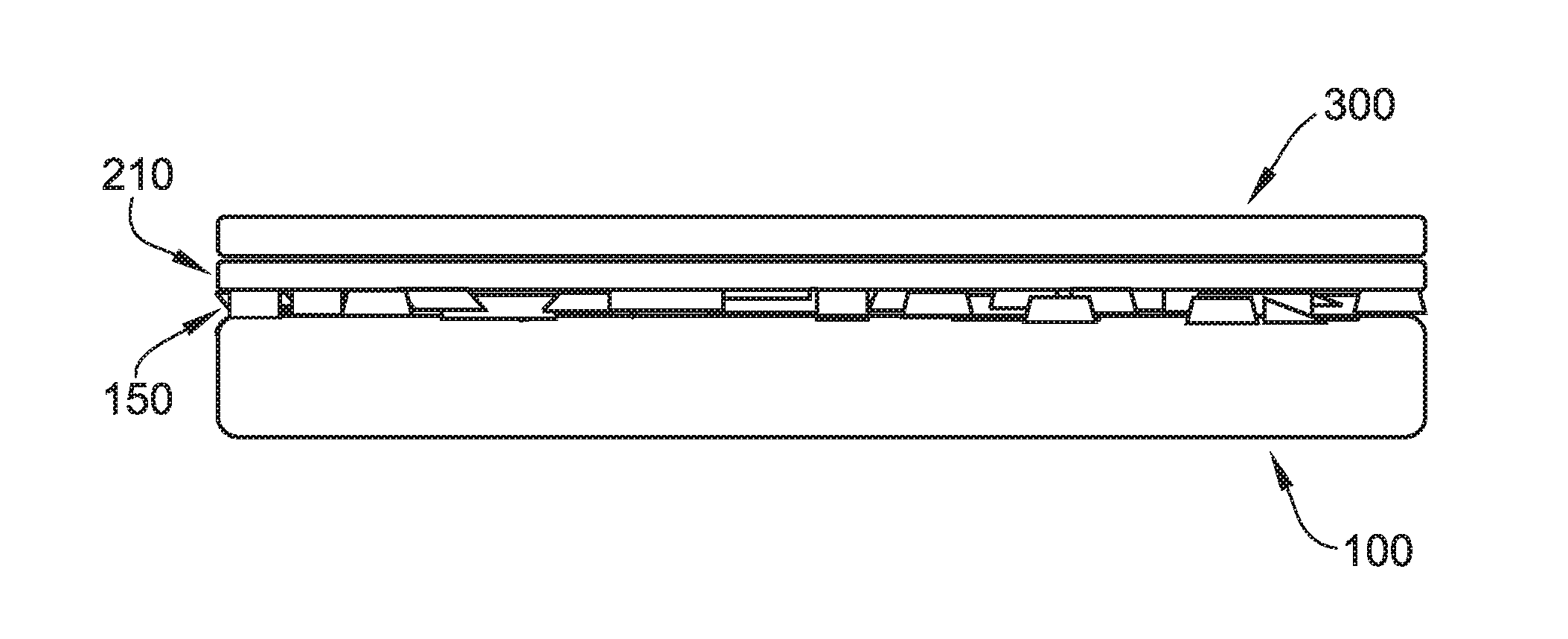
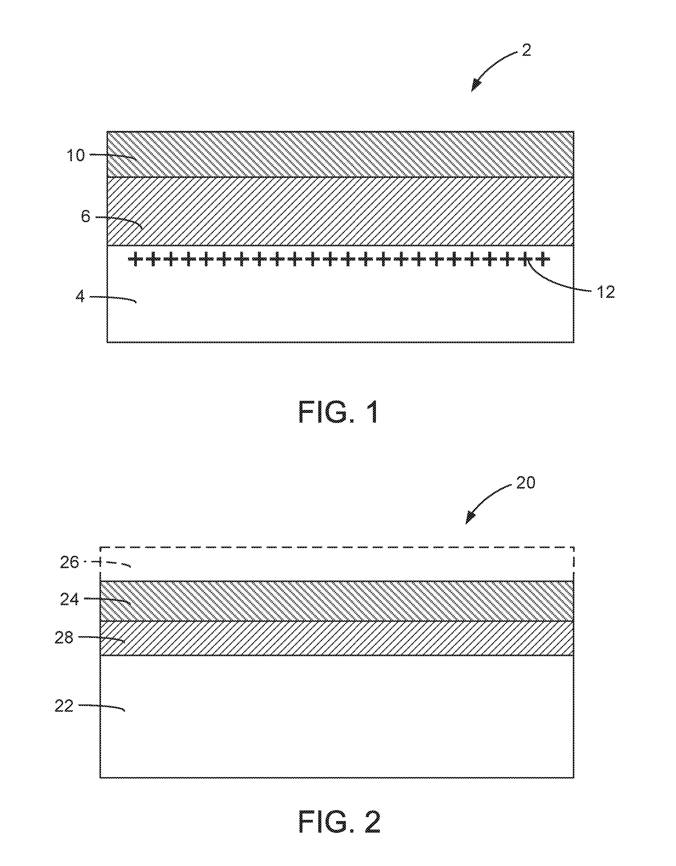
[0011] The use of high resistivity semiconductor-on-insulator (e.g., silicon-on-insulator) wafers for RF related devices such as antenna switches offers benefits over traditional substrates in terms of cost and integration. To reduce parasitic power loss and minimize harmonic distortion inherent when using conductive substrates for high frequency applications it is necessary, but not sufficient, to use substrate wafers with a high resistivity. Accordingly, the resistivity of the handle wafer for an RF device is generally greater than about 500 Ohm-cm. With reference now to FIG. 1, a silicon on insulator structure 2 comprising a very high resistivity silicon wafer 4, a buried oxide (BOX) layer 6, and a silicon device layer 10. Such a substrate is prone to formation of high conductivity charge inversion or accumulation layers 12 at the BOX/handle interface causing generation of free carriers (electrons or holes), which reduce the effective resistivity of the substrate and give rise to parasitic power losses and device nonlinearity when the devices are operated at RF frequencies. These inversion/accumulation layers can be due to BOX fixed charge, oxide trapped charge, interface trapped charge, and even DC bias applied to the devices themselves.
[0012] A method is required therefore to trap the charge in any induced inversion or accumulation layers so that the high resistivity of the substrate is maintained even in the very near surface region. It is known that charge trapping layers (CTL) between the high resistivity handle substrates and the buried oxide (BOX) may improve the performance of RF devices fabricated using SOI wafers. A number of methods have been suggested to form these high interface trap layers. For example, with reference now to FIG. 2, one method of creating a semiconductor-on-insulator structure 20 (e.g., a silicon-on-insulator, or SOI) with a CTL for RF device applications is based on depositing an undoped polycrystalline silicon film 28 on a silicon substrate having high resistivity 22 and then forming a stack of oxide 24 and top silicon layer 26 on it. A polycrystalline silicon layer 28 acts as a high defectivity layer between the silicon substrate 22 and the buried oxide layer 24. See FIG. 2, which depicts a polycrystalline silicon film for use as a charge trapping layer 28 between a high resistivity substrate 22 and the buried oxide layer 24 in a silicon-on-insulator structure 20. An alternative method is the implantation of heavy ions to create a near surface damage layer. Devices, such as radiofrequency devices, are built in the top silicon layer 26.
[0013] It has been shown in academic studies that the polycrystalline silicon layer in between of the oxide and substrate improves the device isolation, decreases transmission line losses and reduces harmonic distortions. See, for example: H. S. Gamble, et al. "Low-loss CPW lines on surface stabilized high resistivity silicon," Microwave Guided Wave Lett., 9(10), pp. 395-397, 1999; D. Lederer, R. Lobet and J.-P. Raskin, "Enhanced high resistivity SOI wafers for RF applications," IEEE Intl. SOI Conf., pp. 46-47, 2004; D. Lederer and J.-P. Raskin, "New substrate passivation method dedicated to high resistivity SOI wafer fabrication with increased substrate resistivity," IEEE Electron Device Letters, vol. 26, no. 11, pp. 805-807, 2005; D. Lederer, B. Aspar, C. Laghae and J.-P. Raskin, "Performance of RF passive structures and SOI MOSFETs transferred on a passivated HR SOI substrate," IEEE International SOI Conference, pp. 29-30, 2006; and Daniel C. Kerr et al. "Identification of RF harmonic distortion on Si substrates and its reduction using a trap-rich layer", Silicon Monolithic Integrated Circuits in RF Systems, 2008. SiRF 2008 (IEEE Topical Meeting), pp. 151-154, 2008.
SUMMARY OF THE INVENTION
[0014] The present invention is directed to a multilayer structure comprising: a single crystal semiconductor handle substrate comprising two major, generally parallel surfaces, one of which is a roughened front surface of the single crystal semiconductor handle substrate and the other of which is a back surface of the single crystal semiconductor handle substrate, a circumferential edge joining the roughened front surface and the back surface of the single crystal semiconductor handle substrate, a central plane between the roughened front surface and the back surface of the single crystal semiconductor handle substrate, and a bulk region between the front and back surfaces of the single crystal semiconductor handle substrate, wherein the single crystal semiconductor handle substrate has a minimum bulk region resistivity of at least about 500 ohm-cm and the roughened front surface of the single crystal semiconductor handle substrate has a surface roughness of at least about 0.01 micrometers as measured according to the root mean square method over a surface area of at least 30 micrometers by 30 micrometers; a charge trapping layer in contact with the roughened front surface single crystal semiconductor handle substrate, the charge trapping layer comprising polycrystalline silicon, the polycrystalline silicon comprising grains having a plurality of crystal orientations; a dielectric layer in contact with the charge trapping layer; and a single crystal semiconductor device layer in contact with the dielectric layer
[0015] The present invention is further directed to a method of forming a multilayer structure, the method comprising: implanting ions selected from the group consisting of He.sup.+, H.sup.+, H.sub.2.sup.+, and any combination thereof through a front surface of a single crystal semiconductor handle substrate to thereby prepare an implant layer in a front surface region of the single crystal semiconductor handle substrate, wherein the single crystal semiconductor handle substrate comprises two major, generally parallel surfaces, one of which is the front surface of the single crystal semiconductor handle substrate and the other of which is a back surface of the single crystal semiconductor handle substrate, a circumferential edge joining the front and back surfaces of the single crystal semiconductor handle substrate, a central plane between the front surface and the back surface of the single crystal semiconductor handle substrate, a front surface region having a depth, D, as measured from the front surface and toward the central plane, and a bulk region between the front and back surfaces of the single crystal semiconductor handle substrate, wherein the single crystal semiconductor handle substrate has a minimum bulk region resistivity of at least about 500 ohm-cm; heating the ion-implanted single crystal semiconductor handle substrate at a temperature and a duration sufficient to from an agglomeration layer in the front surface region of the single crystal semiconductor handle substrate, the agglomeration layer forming at a depth, D1, as measured from the front surface and toward the central plane; mechanically cleaving the single crystal semiconductor handle substrate at the agglomeration layer to thereby expose a roughened front surface of the single crystal semiconductor handle substrate, wherein the roughened front surface has a surface roughness of at least about 0.01 micrometers as measured according to the root mean square method over a surface area of at least 30 micrometers by 30 micrometers; depositing a charge trapping layer on the roughened front surface, the charge trapping layer comprising polycrystalline silicon, the polycrystalline silicon comprising grains having a plurality of crystal orientations; and bonding a dielectric layer on a front surface of a single crystal semiconductor donor substrate to the charge trapping layer to thereby form a bonded structure, wherein the single crystal semiconductor donor substrate comprises two major, generally parallel surfaces, one of which is the front surface of the semiconductor donor substrate and the other of which is a back surface of the semiconductor donor substrate, a circumferential edge joining the front and back surfaces of the semiconductor donor substrate, and a central plane between the front and back surfaces of the semiconductor donor substrate, and further wherein the front surface of the semiconductor donor substrate comprises the dielectric layer.
[0016] Other objects and features will be in part apparent and in part pointed out hereinafter.
BRIEF DESCRIPTION OF THE DRAWINGS
[0017] FIG. 1 is a depiction of a silicon-on-insulator wafer comprising a high resistivity substrate and a buried oxide layer.
[0018] FIG. 2 is a depiction of a silicon-on-insulator wafer according to the prior art, the SOI wafer comprising a polysilicon charge trapping layer between a high resistivity substrate and a buried oxide layer.
[0019] FIGS. 3A through 3G depict a process flow according to some embodiments of the present invention.
DETAILED DESCRIPTION OF THE EMBODIMENT(S) OF THE INVENTION
[0020] According to the present invention, a method is provided for preparing a semiconductor-on-insulator composite structure (SOI, e.g., a silicon-on-insulator composite structure) comprising a charge trapping layer (CTL). The present invention is further directed to a semiconductor-on-insulator composite structure (e.g., a silicon-on-insulator composite structure comprising a charge trapping layer (CTL). In some embodiments, the semiconductor-on-insulator (e.g., silicon-on-insulator) comprises a high resistivity handle substrate comprising a front surface layer prepared with a minimum surface roughness. The charge trapping layer is prepared upon the roughened front surface layer. The charge trapping layer comprises polycrystalline silicon comprising grains having a plurality of crystal orientations.
[0021] In some embodiments, the charge trapping layer prepared upon the roughened front surface layer of the high resistivity handle substrate comprises polycrystalline silicon. Deposition of a charge trapping layer comprising polycrystalline silicon upon a roughened front surface layer yields a CTL layer of enhanced thermal stability. During conventional semiconductor-on-insulator composite structure (e.g., a silicon-on-insulator composite structure) and device fabrication, the CTL is subjected to high temperature anneals which may cause at least partial recrystallization of the polycrystalline silicon CTL material. The recrystallization is seeded by the substrate and occurs at multiple polycrystalline silicon grains which grow in size and merge with grain boundaries causing annihilation of individual crystal grains because the grains acquire the same crystal orientation as the surface of the substrate. According to the method of the present invention, the front surface layer of the handle substrate is roughened and has different orientation at localized spots. The polycrystalline silicon recrystallizes, during a high temperature process step, in grains on the substrate surface with different crystallographic orientations and having different activation and grain growth rate. As a result, even a recrystallized polycrystalline silicon CTL has highly defective structure and preserves the intended charge trapping efficiency. Accordingly, the rough interface in the structure may trap charges and effectively scatters charge carriers in silicon. Therefore, in case of formation of inversion or charge accumulation layers at the substrate surface, the parasitic conduction of the substrate is lower. Accordingly, the RF performance of the charge trapping layer prepared according to the method of the present invention.
I. Semiconductor Handle Substrate and Semiconductor Donor Substrate
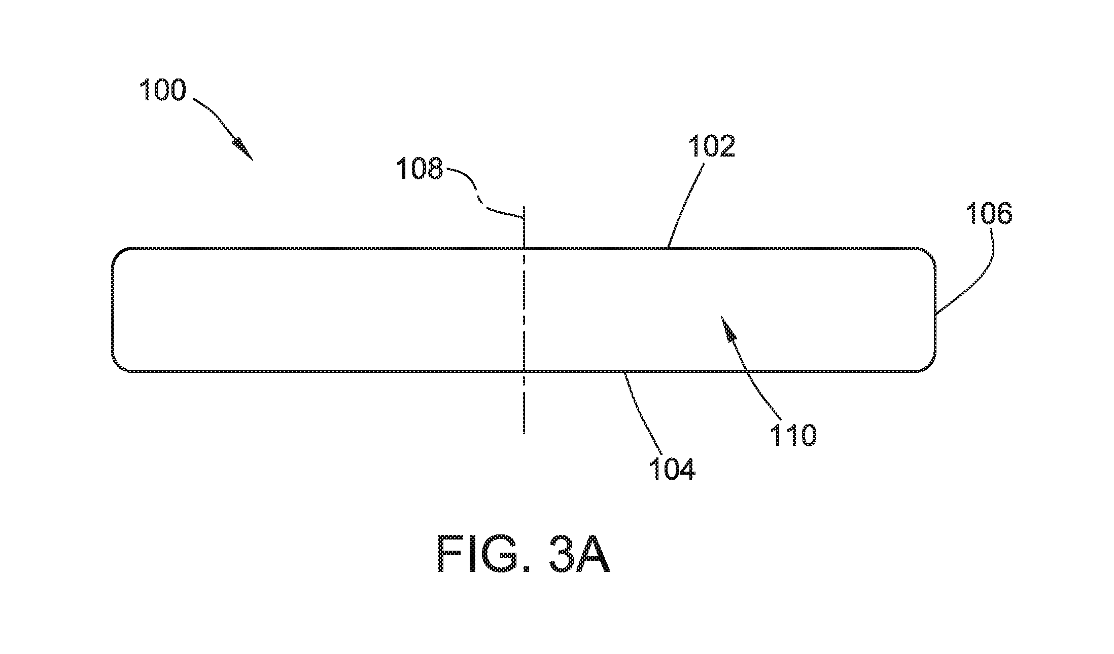
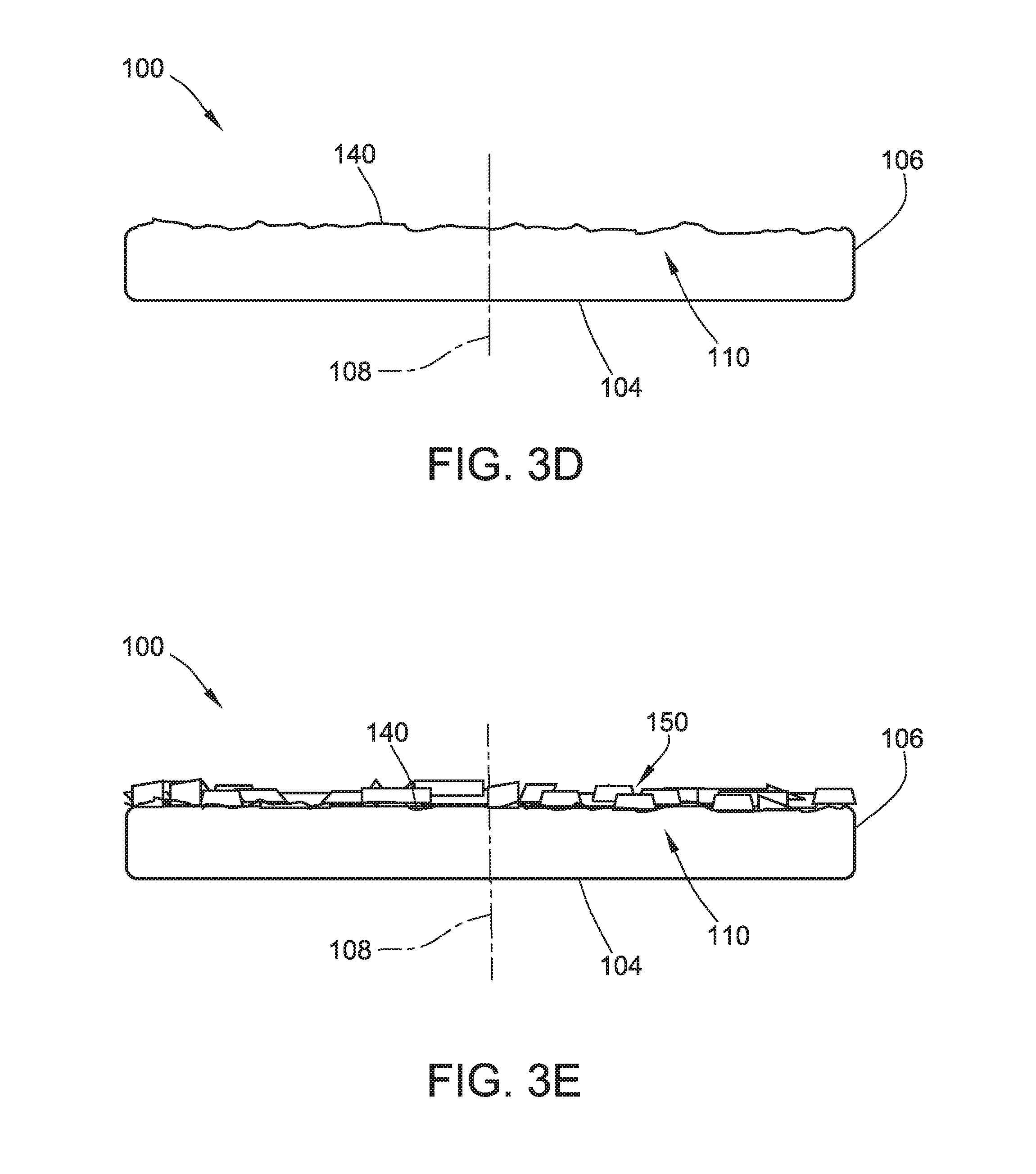
[0022] The substrates for use in the present invention include a semiconductor handle substrate, e.g., a single crystal semiconductor handle wafer and a semiconductor donor substrate, e.g., a single crystal semiconductor donor wafer. The semiconductor device layer in a semiconductor-on-insulator composite structure is derived from the single crystal semiconductor donor wafer. The semiconductor device layer may be transferred onto the semiconductor handle substrate by wafer thinning techniques such as etching a semiconductor donor substrate or by cleaving a semiconductor donor substrate comprising a damage plane. FIGS. 3A through 3G depict a process flow according to some embodiments of the present invention.
[0023] With reference to FIG. 3A, an exemplary, non-limiting single crystal semiconductor handle wafer 100 is depicted. In general, the single crystal semiconductor handle wafer 100 comprises two major, generally parallel surfaces. One of the parallel surfaces is a front surface 102 of the single crystal semiconductor handle wafer 100, and the other parallel surface is a back surface 104 of the single crystal semiconductor handle wafer 100. The single crystal semiconductor handle wafer 100 comprises a circumferential edge 106 joining the front and back surfaces 102, 104. The single crystal semiconductor handle wafer 100 comprise a central axis 108 perpendicular to the two major, generally parallel surfaces 102, 104 and also perpendicular to a central plane defined by the points midway between the front and back surfaces 102, 104. The single crystal semiconductor handle wafer 100 comprises a bulk region 110 between the two major, generally parallel surfaces 102, 104. Since semiconductor wafers, e.g., silicon wafers, typically have some total thickness variation (TTV), warp, and bow, the midpoint between every point on the front surface 102 and every point on the back surface 104 may not precisely fall within a plane. As a practical matter, however, the TTV, warp, and bow are typically so slight that to a close approximation the midpoints can be said to fall within an imaginary central plane which is approximately equidistant between the front and back surfaces 102, 104.
[0024] Prior to any operation as described herein, the front surface 102 and the back surface 104 of the single crystal semiconductor handle wafer 100 may be substantially identical. A surface is referred to as a "front surface" or a "back surface" merely for convenience and generally to distinguish the surface upon which the operations of method of the present invention are performed. In the context of the present invention, a "front surface" of a single crystal semiconductor handle wafer 100, e.g., a single crystal silicon handle wafer, refers to the major surface of the substrate that becomes an interior surface of the bonded structure. Accordingly, a "back surface" of a single crystal semiconductor handle wafer 100, e.g., a handle wafer, refers to the major surface that becomes an exterior surface of the bonded structure. Similarly, a "front surface" of a single crystal semiconductor donor substrate, e.g., a single crystal silicon donor wafer, refers to the major surface of the single crystal semiconductor donor substrate that becomes an interior surface of the bonded structure, and a "back surface" of a single crystal semiconductor donor substrate, e.g., a single crystal silicon donor wafer, refers to the major surface that becomes an exterior surface of the bonded structure. Upon completion of conventional bonding and wafer thinning steps, the single crystal semiconductor donor substrate forms the semiconductor device layer of the semiconductor-on-insulator (e.g., silicon-on-insulator) composite structure.
[0025] The single crystal semiconductor handle substrate and the single crystal semiconductor donor substrate may be single crystal semiconductor wafers. In preferred embodiments, the semiconductor wafers comprise a material selected from the group consisting of silicon, silicon carbide, silicon germanium, gallium arsenide, gallium nitride, indium phosphide, indium gallium arsenide, germanium, and combinations thereof. The single crystal semiconductor wafers, e.g., the single crystal silicon handle wafer and single crystal silicon donor wafer, of the present invention typically have a nominal diameter of at least about 150 mm, at least about 200 mm, at least about 300 mm, or at least about 450 mm. Wafer thicknesses may vary from about 250 micrometers to about 1500 micrometers, such as between about 300 micrometers and about 1000 micrometers, suitably within the range of about 500 micrometers to about 1000 micrometers. In some specific embodiments, the wafer thickness may be about 725 micrometers. In some embodiments, the wafer thickness may be about 775 micrometers.
[0026] In particularly preferred embodiments, the single crystal semiconductor wafers comprise single crystal silicon wafers which have been sliced from a single crystal ingot grown in accordance with conventional Czochralski crystal growing methods or float zone growing methods. Such methods, as well as standard silicon slicing, lapping, etching, and polishing techniques are disclosed, for example, in F. Shimura, Semiconductor Silicon Crystal Technology, Academic Press, 1989, and Silicon Chemical Etching, (J. Grabmaier ed.) Springer-Verlag, N.Y., 1982 (incorporated herein by reference). Preferably, the wafers are polished and cleaned by standard methods known to those skilled in the art. See, for example, W. C. O'Mara et al., Handbook of Semiconductor Silicon Technology, Noyes Publications. If desired, the wafers can be cleaned, for example, in a standard SC1/SC2 solution. In some embodiments, the single crystal silicon wafers of the present invention are single crystal silicon wafers which have been sliced from a single crystal ingot grown in accordance with conventional Czochralski ("Cz") crystal growing methods, typically having a nominal diameter of at least about 150 mm, at least about 200 mm, at least about 300 mm, or at least about 450 mm. Preferably, both the single crystal silicon handle wafer and the single crystal silicon donor wafer have mirror-polished front surface finishes that are free from surface defects, such as scratches, large particles, etc. Wafer thickness may vary from about 250 micrometers to about 1500 micrometers, such as between about 300 micrometers and about 1000 micrometers, suitably within the range of about 500 micrometers to about 1000 micrometers. In some specific embodiments, the wafer thickness may be between about 725 micrometers and about 800 micrometers, such as between about 750 micrometers and about 800 micrometers. In some embodiments, the wafer thickness may be about 725 micrometers. In some embodiments, the wafer thickness may be about 775 micrometers.
[0027] In some embodiments, the single crystal semiconductor wafers, i.e., single crystal semiconductor handle wafer and single crystal semiconductor donor wafer, comprise interstitial oxygen in concentrations that are generally achieved by the Czochralski-growth method. In some embodiments, the single crystal semiconductor wafers comprise oxygen in a concentration between about 4 PPMA and about 18 PPMA. In some embodiments, the semiconductor wafers comprise oxygen in a concentration between about 10 PPMA and about 35 PPMA. In some embodiments, the single crystal silicon wafer comprises oxygen in a concentration of no greater than about 10 PPMA. Interstitial oxygen may be measured according to SEMI MF 1188-1105.
[0028] The single crystal semiconductor handle wafer 100 may have any resistivity obtainable by the Czochralski or float zone methods. Accordingly, the resistivity of the single crystal semiconductor handle wafer 100 is based on the requirements of the end use/application of the structure of the present invention. The resistivity may therefore vary from milliohm or less to megaohm or more. In some embodiments, the single crystal semiconductor handle wafer 100 comprises a p-type or an n-type dopant. Suitable dopants include boron (p type), gallium (p type), phosphorus (n type), antimony (n type), and arsenic (n type). The dopant concentration is selected based on the desired resistivity of the handle wafer. In some embodiments, the single crystal semiconductor handle substrate comprises a p-type dopant. In some embodiments, the single crystal semiconductor handle substrate is a single crystal silicon wafer comprising a p-type dopant, such as boron.
[0029] In some embodiments, the single crystal semiconductor handle wafer 100 has a relatively low minimum bulk resistivity, such as below about 100 ohm-cm, below about 50 ohm-cm, below about 1 ohm-cm, below about 0.1 ohm-cm, or even below about 0.01 ohm-cm. In some embodiments, the single crystal semiconductor handle substrate 100 has a relatively low minimum bulk resistivity, such as below about 100 ohm-cm, or between about 1 ohm-cm and about 100 ohm-cm. Low resistivity wafers may comprise electrically active dopants, such as boron (p type), gallium (p type), aluminum (p type), indium (p type), phosphorus (n type), antimony (n type), and arsenic (n type).
[0030] In some embodiments, the single crystal semiconductor handle wafer 100 has a relatively high minimum bulk resistivity. High resistivity wafers are generally sliced from single crystal ingots grown by the Czochralski method or float zone method. High resistivity wafers may comprise electrically active dopants, such as boron (p type), gallium (p type), aluminum (p type), indium (p type), phosphorus (n type), antimony (n type), and arsenic (n type), in generally very low concentrations. Cz-grown silicon wafers may be subjected to a thermal anneal at a temperature ranging from about 600.degree. C. to about 1000.degree. C. in order to annihilate thermal donors caused by oxygen that are incorporated during crystal growth. In some embodiments, the single crystal semiconductor handle wafer has a minimum bulk resistivity of at least 100 Ohm-cm, or even at least about 500 Ohm-cm, such as between about 100 Ohm-cm and about 100,000 Ohm-cm, or between about 500 Ohm-cm and about 100,000 Ohm-cm, or between about 1000 Ohm-cm and about 100,000 Ohm-cm, or between about 500 Ohm-cm and about 10,000 Ohm-cm, or between about 750 Ohm-cm and about 10,000 Ohm-cm, between about 1000 Ohm-cm and about 10,000 Ohm-cm, between about 1000 Ohm-cm and about 6000 ohm-cm, between about 2000 Ohm-cm and about 10,000 Ohm-cm, between about 3000 Ohm-cm and about 10,000 Ohm-cm, or between about 3000 Ohm-cm and about 5,000 Ohm-cm. In some preferred embodiments, the single crystal semiconductor handle substrate has a bulk resistivity between about 1000 Ohm-cm and about 6,000 Ohm-cm. Methods for preparing high resistivity wafers are known in the art, and such high resistivity wafers may be obtained from commercial suppliers, such as SunEdison Semiconductor Ltd. (St. Peters, Mo.; formerly MEMC Electronic Materials, Inc.).
[0031] The single crystal semiconductor handle wafer 100 may comprise single crystal silicon. The single crystal semiconductor handle wafer 100 may have, for example, any of (100), (110), or (111) crystal orientation, and the choice of crystal orientation may be dictated by the end use of the structure.
[0032] Optionally, the front surface 102, the back surface 104, or both may be oxidized according to methods known in the art. Oxidation may be accomplished by means known in the art, such as thermal oxidation (in which some portion of the deposited semiconductor material film will be consumed), CVD oxide deposition, or by exposure to a standard cleaning solution, such as an SC1/SC2 cleaning solution. The oxidation layer on the front surface 102, the back surface 104, or both may be may be at least about 1 nanometer thick, such as between about 10 nanometers and about 5000 nanometers thick, such as between about 100 nanometers and about 1000 nanometers, or between about 200 nanometers and about 400 nanometers. In some embodiments, the oxidation layer is relatively thin, such as between about 5 angstroms and about 25 angstroms, such as between about 10 angstroms and about 15 angstroms. Thin oxide layers can be obtained by exposure to a standard cleaning solution, such as an SC1/SC2 cleaning solution.
II. Formation of Roughened Front Surface Layer
[0033] According to the method of the present invention, and with reference to FIGS. 3A through 3G, the front surface 102 of the starting single crystal semiconductor handle substrate 100 is roughened. A roughened front surface may be obtained by ion implantation, anneal to agglomerate the implanted species, and cleaving.
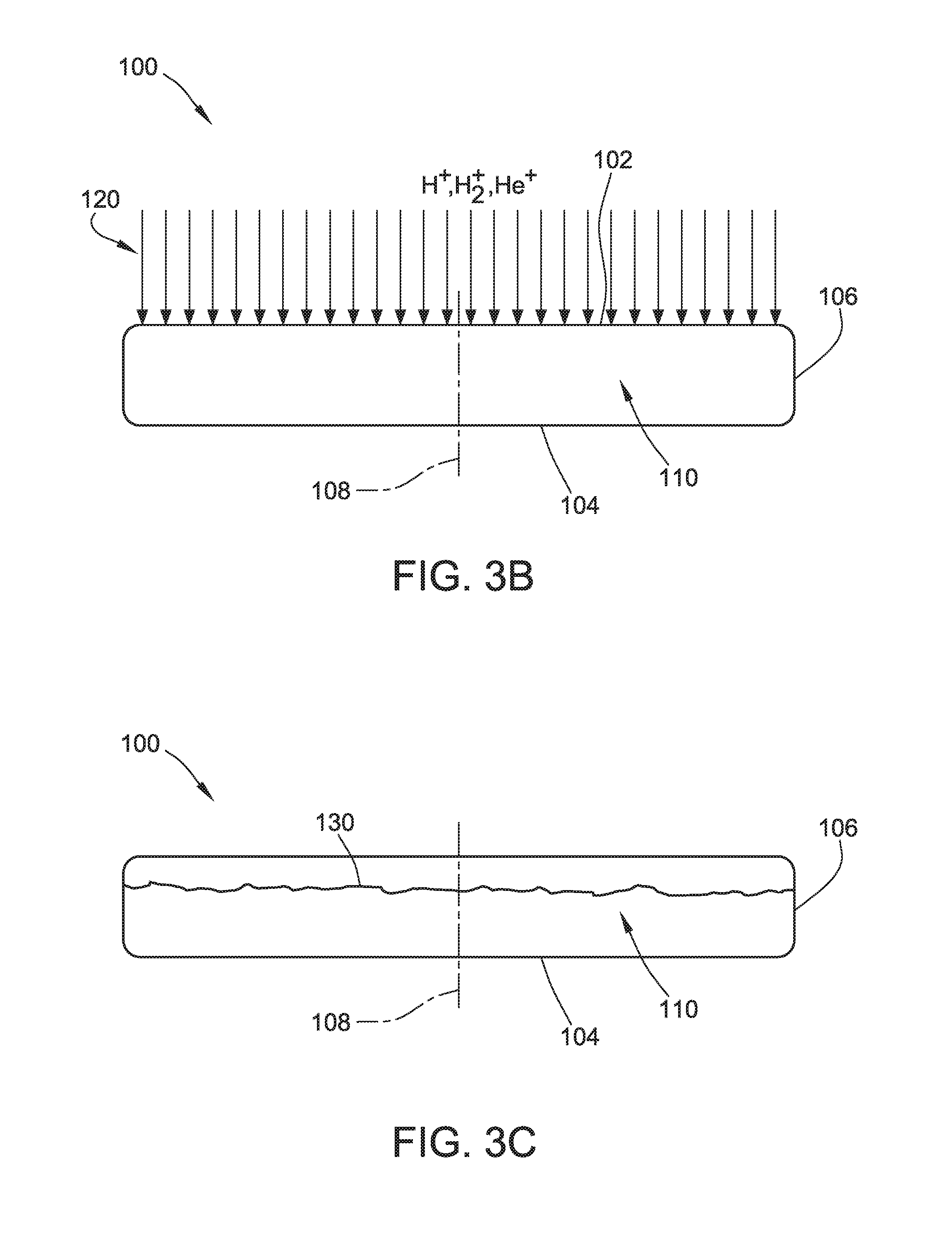
[0034] With Reference to FIGS. 3A and 3B, ion implantation 120 through the front surface 102 of the starting single crystal semiconductor handle substrate 100 may be carried out in a commercially available instrument, such as an Applied Materials Quantum II, a Quantum LEAP, or a Quantum X. Implanted ions may include He.sup.+, H.sup.+, H.sub.2.sup.+, and any combination thereof. Ion implantation 120 is carried out at a density and duration sufficient to form a damage layer in the single crystal semiconductor handle substrate. Implant density may range from about 10.sup.12 ions/cm.sup.2 to about 10.sup.17 ions/cm.sup.2, such as from about 10.sup.14 ions/cm.sup.2 to about 10.sup.17 ions/cm.sup.2, such as from about 10.sup.15 ions/cm.sup.2 to about 10.sup.16 ions/cm.sup.2. Implant energies may range from about 1 keV to about 3,000 keV, such as from about 10 keV to about 3,000 keV. Implant energies may range from about 1 keV to about 3,000 keV, such as from about 5 keV to about 1,000 keV, or from about 5 keV to about 200 keV, or from 5 keV to about 100 keV, or from 5 keV to about 80 keV. The ions may be implanted to a depth between about 100 angstroms and about 20,000 angstroms, such as between about 1000 angstroms and about 3000 angstroms. In some embodiments it may be desirable to subject the ion implanted front surface 102 of the starting single crystal semiconductor handle substrate 100 to a clean after the implant. In some preferred embodiments, the clean could include a Piranha clean followed by a DI water rinse and SC1/SC2 cleans.
[0035] With reference to FIG. 3C, after ion implantation, the implanted single crystal semiconductor handle substrate 102 is subjected to a thermal anneal to out-diffuse the implanted species and form a layer 130 of agglomerates. A conventional furnace, such as an ASM A 400, may be used for the thermal anneal. The temperature of the thermal anneal may range from about 300.degree. C. to about 1200.degree. C., such as between about 700.degree. C. to about 1200.degree. C. or between about 300.degree. C. to about 450.degree. C., and the duration may range from about 10 minutes to about 2 hours, such as between about 10 minutes and about 1 hour. Implantation 120 of He.sup.+, H.sup.+, H.sub.2.sup.+, and any combination thereof followed by heat treatment causes out-diffusion of the implanted species, which thereby forms a region or layer 130 of agglomerates. The layer 130 of agglomerates is generally a few nanometers thick, such as between 1 nanometer and about 1000 nanometers, or between about 10 nanometers and about 500 nanometers.
[0036] After ion implantation and thermal treatment, wafer cleaning is optional. If desired, the wafers can be cleaned, for example, in a standard SC1/SC2 solution.
[0037] After the thermal anneal, a region at the front of the single crystal semiconductor handle substrate 100 is cleaved from the substrate 100 at the layer 130 of agglomerates. Cleaving may occur according to techniques known in the art. In some embodiments, the single crystal semiconductor handle substrate 100 may be placed in a conventional cleave station affixed to stationary suction cups on one side and affixed by additional suction cups on a hinged arm on the other side. A crack is initiated near the suction cup attachment and the movable arm pivots about the hinge cleaving the wafer apart. Cleaving removes a portion from the front of the single crystal semiconductor handle substrate 100, thereby exposing the layer 130 of agglomerates and preparing a roughened front surface 140. See FIG. 3D.
[0038] After cleaving, wafer cleaning is optional. If desired, the wafers can be cleaned, for example, in a standard SC1/SC2 solution.
[0039] Other techniques for preparing a roughened front surface 140 may be utilized. For example, the front surface of the of the semiconductor handle wafer 100 (e.g., a silicon wafer) may be subjected to fine grinding or ion milling/implantation or any other method to initiate surface defects/damage. In another technique, the front surface may be subjected to fine grinding and anisotropic wet chemical etch, e.g., in KOH, NH.sub.4OH, etc. to expose Si(111) facets. Still further, fine grinding (followed by SC1/SC2 clean) and a hydrogen chloride vapor etch in a silicon wafer processing reactor at low temperatures, such as between about 700.degree. C. and about 850.degree. C. Finally, the front surface of the of the semiconductor handle wafer 100 may be etched in a silicon wafer processing reactor at low temperatures, such as between about 700.degree. C. and about 850.degree. C. The native oxide on the wafer surface serves as a masking layer for creating faceted pits.
[0040] In some embodiments, the roughened front surface 140 of the semiconductor handle wafer 100 (e.g., a silicon wafer) is oxidized. Oxidation of the roughened surface is optional and generally depends on the trap layer deposition conditions. In embodiments wherein the charge trapping layer is deposited by LP (lower pressure) CVD at low temperature, such as less than 650.degree. C., with precursors such as SiH.sub.4, oxidation may not be necessary. In embodiments wherein the charge trapping layer is deposited using SiHCl.sub.3 with CVD, the thin oxide layer of between about 1 nanometer and about 5 nanometers may be deposited to improve polynucleation. Oxidation may be accomplished by means known in the art, such as thermal oxidation (in which some portion of the deposited semiconductor material film will be consumed) or CVD oxide deposition. In some embodiments, the single crystal semiconductor handle substrate, e.g., a single crystal silicon handle wafer, may be thermally oxidized in a furnace such as an ASM A400. The temperature may range from 750.degree. C. to 1200.degree. C. in an oxidizing ambient. The oxidizing ambient atmosphere can be a mixture of inert gas, such as Ar or N.sub.2, and O.sub.2. The oxygen content may vary from 1 to 10 percent, or higher. In some embodiments, the oxidizing ambient atmosphere may be up to 100% (a "dry oxidation"). In an exemplary embodiment, single crystal semiconductor handle wafer 100 having the roughened front surface 140 may be loaded into a vertical furnace, such as an A400. The temperature is ramped to the oxidizing temperature with a mixture of N.sub.2 and O.sub.2. After the desired oxide thickness has been obtained, the O.sub.2 is turned off and the furnace temperature is reduced and wafers are unloaded from the furnace. The oxidation layer on the roughened front surface 140 may be between about 1 nanometer and about 5000 nanometers thick, between about 10 nanometers and about 5000 nanometers thick, such as between about 100 nanometers and about 1000 nanometers, or between about 200 nanometers and about 400 nanometers, or between about 1 nanometer and about 100 nanometers.
[0041] According to the method of the present invention, the roughened front surface 140 of the single crystal semiconductor handle wafer 100 has a surface roughness as measured by the root mean square method over a surface area of 30 micrometers by 30 micrometers of at least about 0.01 micrometers, such as least about 0.1 micrometers, such as between about 0.1 micrometer and about 1 micrometer. The root mean squared is calculated according to the following equation:
R q = 1 n i = 1 n y i 2 ##EQU00001##
[0042] The roughness profile contains ordered, equally spaced points along the trace, and y.sub.i is the vertical distance from the mean line to the data point. Roughness is measured over a 30 micrometer by 30 micrometer surface area.
III. Deposition of Charge Trapping Layer
[0043] According to the method of the present invention and with reference to FIG. 3E, semiconductor material is deposited onto the roughened front surface 140 of the single crystal semiconductor handle wafer 100. Semiconductor material suitable for use in forming a charge trapping layer 150 in a semiconductor-on-insulator device is suitably capable of forming a highly defective layer in the fabricated device. Such materials include polycrystalline semiconductor materials and amorphous semiconductor materials. Materials that may be polycrystalline or amorphous include silicon (Si), silicon germanium (SiGe), silicon doped with carbon (SiC), and germanium (Ge). Polycrystalline semiconductor, e.g., polycrystalline silicon, denotes a material comprising small silicon crystals having random crystal orientations. Polycrystalline silicon grains may be as small in size as about 20 nanometers. The polycrystalline silicon grains may be as large as 1000 nanometers. In some embodiments, the polycrystalline silicon grains may have an average size between about 20 nanometers and about 500 nanometers. According to the method of the present invention, the smaller the crystal grain size of polycrystalline silicon deposited the higher the defectivity in the charge trapping layer. Amorphous semiconductor, e.g., amorphous silicon, comprises a non-crystalline allotropic form of silicon, which lacks short range and long range order. Silicon grains having crystallinity over no more than about 10 nanometers may also be considered essentially amorphous. Silicon germanium comprises an alloy of silicon germanium in any molar ratio of silicon and germanium. Silicon doped with carbon comprises a compound of silicon and carbon, which may vary in molar ratio of silicon and carbon. Preferably, the charge trapping layer 150 has a resistivity at least about 1000 Ohm-cm, or at least about 3000 Ohm-cm, such as between about 1000 Ohm-cm and about 100,000 Ohm-cm, between about 1000 Ohm-cm and about 10,000 Ohm-cm, between about 2000 Ohm-cm and about 10,000 Ohm-cm, between about 3000 Ohm-cm and about 10,000 Ohm-cm, or between about 3000 Ohm cm and about 5,000 Ohm-cm.
[0044] The material for deposition onto the roughened front surface 140 of the single crystal semiconductor handle wafer 100 may be deposited by means known in the art. For example, the semiconductor material may be deposited using metalorganic chemical vapor deposition (MOCVD), physical vapor deposition (PVD), chemical vapor deposition (CVD), low pressure chemical vapor deposition (LPCVD), plasma enhanced chemical vapor deposition (PECVD), or molecular beam epitaxy (MBE). Silicon precursors for LPCVD or PECVD include methyl silane, silicon tetrahydride (silane), trisilane, disilane, pentasilane, neopentasilane, tetrasilane, dichlorosilane (SiH.sub.2Cl.sub.2), silicon tetrachloride (SiCl.sub.4), among others. For example, polycrystalline silicon may be deposited onto the roughened front surface 140 of the single crystal semiconductor handle wafer 100 by pyrolyzing silane (SiH.sub.4) in a temperature range between about 550.degree. C. and about 690.degree. C., such as between about 580.degree. C. and about 650.degree. C. The chamber pressure may range from about 70 to about 400 mTorr. Amorphous silicon may be deposited by plasma enhanced chemical vapor deposition (PECVD) at temperatures generally ranging between about 75.degree. C. and about 300.degree. C. Silicon germanium, particularly amorphous silicon germanium, may be deposited at temperatures up to about 300.degree. C. by chemical vapor deposition by including organogermanium compounds, such as isobutylgermane, alkylgermanium trichlorides, and dimethylaminogermanium trichloride. Silicon doped with carbon may be deposited by thermal plasma chemical vapor deposition in epitaxial reactors using precursors such as silicon tetrachloride and methane. Suitable carbon precursors for CVD or PECVD include methylsilane, methane, ethane, ethylene, among others. For LPCVD deposition, methylsilane is a particularly preferred precursor since it provides both carbon and silicon. For PECVD deposition, the preferred precursors include silane and methane. In some embodiments, the silicon layer may comprise a carbon concentration of at least about 1% on an atomic basis, such as between about 1% on an atomic basis and about 10% on an atomic basis. The overall thickness of the charge trapping layer 150 may be between about 0.3 micrometers and about 5 micrometers, such as between about 0.3 micrometers and about 3 micrometers, such as between about 0.3 micrometers and about 2 micrometers, between about 1 micrometers and about 3 micrometers, or between about 2 micrometers and about 3 micrometers.
[0045] Due to the roughness of the roughened front surface 140 of the single crystal semiconductor handle wafer 100, the charge trapping layer 150 comprising polycrystalline silicon and/or the other materials comprises grains having a plurality of orientations. Moreover, the grains may be randomly oriented. See FIG. 3E, which depicts an exemplary, non-limiting illustration of the polycrystalline silicon grains having a plurality of shapes, sizes, and orientations in the charge trapping layer 150. The depiction of FIG. 3E is meant to be illustrative of random orientation of crystalline grains. In some embodiments, the plurality of crystal orientations of the polycrystalline silicon comprising grains comprise at least two orientations selected from the group consisting of (111), (100), and (110). The random orientations, sizes, and shapes enhance the defectivity and effectiveness of the charge trapping layer. The grain size can be measured by x-ray diffraction, raman spectroscopy, atomic force microscopy, and other techniques for surface measurement. The typical grain size may range from between about 10 nanometers to about 3 micrometers, such as between about 10 nanometers and about 1 micrometer, or between about 1 micrometer and about 2 micrometers. These grain sizes are suitable for the purpose of trapping charge. Uniform grain size across the charge trapping layer is preferred rather than a wide distribution of grain sizes.
[0046] In some embodiments, the charge trapping layer 150 comprising polycrystalline silicon and/or the other materials disclosed herein may be subjected to chemical mechanical polishing ("CMP"). Chemical mechanical polishing may occur by methods known in the art. The post-CMP roughness, as measured by AFM, is preferably less than about 0.5 nanometers (root mean square), preferably between about 0.1 nanometer and about 0.3 nanometer. This roughness is advantageous for the subsequent successful bonding to the donor substrate and layer transfer.
[0047] In some embodiments, the charge trapping layer 150 is oxidized. Oxidizing is optional and generally depends upon the requirements of the final semiconductor on insulator structure. Oxidation may be accomplished by means known in the art, such as thermal oxidation (in which some portion of the deposited semiconductor material film will be consumed) or CVD oxide deposition. In some embodiments, the charge trapping layer 150 may be thermally oxidized in a furnace such as an ASM A400. The temperature may range from 750.degree. C. to 1200.degree. C. in an oxidizing ambient. The oxidizing ambient atmosphere can be a mixture of inert gas, such as Ar or N.sub.2, and O.sub.2. The oxygen content may vary from 1 to 10 percent, or higher. In some embodiments, the oxidizing ambient atmosphere may be up to 100% (a "dry oxidation"). In an exemplary embodiment, single crystal semiconductor handle wafer 100 comprising the charge trapping layer 150 may be loaded into a vertical furnace, such as an A400. The temperature is ramped to the oxidizing temperature with a mixture of N.sub.2 and O.sub.2. After the desired oxide thickness has been obtained, the O.sub.2 is turned off and the furnace temperature is reduced and wafers are unloaded from the furnace. The oxidation layer on the charge trapping layer 150 may be between about 10 nanometers and about 5000 nanometers thick, such as between about 100 nanometers and about 1000 nanometers, or between about 200 nanometers and about 400 nanometers.
IV. Preparation of the Bonded Structure
[0048] With reference to FIG. 3F, the high resistivity single crystal semiconductor handle substrate 100, e.g. a single crystal semiconductor handle wafer such as a single crystal silicon handle wafer, prepared according to the method described herein comprising a roughened front surface 140 and charge trapping layer 150 is next bonded a semiconductor donor substrate 200, e.g., a single crystal semiconductor donor wafer, which is prepared according to conventional layer transfer methods. The single crystal semiconductor donor substrate 200 may be a single crystal semiconductor wafer. In preferred embodiments, the semiconductor wafer comprises a material selected from the group consisting of silicon, silicon carbide, silicon germanium, gallium arsenide, gallium nitride, indium phosphide, indium gallium arsenide, germanium, and combinations thereof. Depending upon the desired properties of the final integrated circuit device, the single crystal semiconductor (e.g., silicon) donor wafer 200 may comprise a dopant selected from the group consisting of boron, arsenic, and phosphorus. The resistivity of the single crystal semiconductor (e.g., silicon) donor wafer may range from 1 to 50 Ohm-cm, typically, from 5 to 25 Ohm-cm. The single crystal semiconductor donor wafer 200 may be subjected to standard process steps including oxidation, implant, and post implant cleaning. Accordingly, a semiconductor donor substrate 200, such as a single crystal semiconductor wafer of a material that is conventionally used in preparation of multilayer semiconductor structures, e.g., a single crystal silicon donor wafer, that has been etched and polished and optionally oxidized, is subjected to ion implantation to form a damage layer in the donor substrate.
[0049] In some embodiments, the semiconductor donor substrate 200 comprises a dielectric layer 210. Suitable dielectric layers may comprise a material selected from among silicon dioxide, silicon nitride, hafnium oxide, titanium oxide, zirconium oxide, lanthanum oxide, barium oxide, and a combination thereof. In some embodiments, the dielectric layer 210 comprises an oxide layer having a thickness of at least about 10 nanometer thick, such as between about 10 nanometers and about 10,000 nanometers, between about 10 nanometers and about 5,000 nanometers, or between about 100 nanometers and about 400 nanometers.
[0050] In some embodiments, the front surface of the single crystal semiconductor donor substrate 200 (e.g., a single crystal silicon donor substrate) may be thermally oxidized (in which some portion of the deposited semiconductor material film will be consumed) to prepare the semiconductor oxide film, or the semiconductor oxide (e.g., silicon dioxide) film may be grown by CVD oxide deposition. In some embodiments, the front surface of the single crystal semiconductor donor substrate 200 may be thermally oxidized in a furnace such as an ASM A400 in the same manner described above. In some embodiments, the donor substrates are oxidized to provide an oxide layer on the front surface layer of at least about 10 nanometer thick, such as between about 10 nanometers and about 10,000 nanometers, between about 10 nanometers and about 5,000 nanometers, or between about 100 nanometers and about 400 nanometers.
[0051] Ion implantation of a donor structure to thereby prepare a cleave plane may be carried out in a commercially available instrument, such as an Applied Materials Quantum II, a Quantum LEAP, or a Quantum X. Implanted ions may include He.sup.+, H.sup.+, H.sub.2.sup.+, and any combination thereof. Ion implantation is carried out as a density and duration sufficient to form a damage layer in the semiconductor donor substrate. Implant density may range from about 10.sup.12 ions/cm.sup.2 to about 10.sup.17 ions/cm.sup.2, such as from about 10.sup.14 ions/cm.sup.2 to about 10.sup.17 ions/cm.sup.2, such as from about 10.sup.15 ions/cm.sup.2 to about 10.sup.16 ions/cm.sup.2. Implant energies may range from about 1 keV to about 3,000 keV, such as from about 10 keV to about 3,000 keV. Implant energies may range from about 1 keV to about 3,000 keV, such as from about 5 keV to about 1,000 keV, or from about 5 keV to about 200 keV, or from 5 keV to about 100 keV, or from 5 keV to about 80 keV. The ions may be implanted to a depth between about 100 angstroms and about 20,000 angstroms, such as between about 1000 angstroms and about 3000 angstroms. In some embodiments it may be desirable to subject the single crystal semiconductor donor wafers, e.g., single crystal silicon donor wafers, to a clean after the implant. In some preferred embodiments, the clean could include a Piranha clean followed by a DI water rinse and SC1/SC2 cleans.
[0052] In some embodiments of the present invention, the single crystal semiconductor donor substrate 200 having an ion implant region therein formed by He.sup.+, H.sup.+, H.sub.2.sup.+, and any combination thereof ion implant is annealed at a temperature sufficient to form a thermally activated cleave plane in the single crystal semiconductor donor substrate. An example of a suitable tool might be a simple Box furnace, such as a Blue M model. In some preferred embodiments, the ion implanted single crystal semiconductor donor substrate is annealed at a temperature of from about 200.degree. C. to about 350.degree. C., from about 225.degree. C. to about 325.degree. C., preferably about 300.degree. C. Thermal annealing may occur for a duration of from about 2 hours to about 10 hours, such as from about 2 hours to about 8 hours. Thermal annealing within these temperatures ranges is sufficient to form a thermally activated cleave plane. After the thermal anneal to activate the cleave plane, the single crystal semiconductor donor substrate surface is preferably cleaned.
[0053] In some embodiments, the ion-implanted and optionally cleaned and optionally annealed single crystal semiconductor donor substrate is subjected to oxygen plasma and/or nitrogen plasma surface activation. In some embodiments, the oxygen plasma surface activation tool is a commercially available tool, such as those available from EV Group, such as EVG.RTM.810LT Low Temp Plasma Activation System. The ion-implanted and optionally cleaned single crystal semiconductor donor wafer is loaded into the chamber. The chamber is evacuated and backfilled with O.sub.2 to a pressure less than atmospheric to thereby create the plasma. The single crystal semiconductor donor wafer is exposed to this plasma for the desired time, which may range from about 1 second to about 120 seconds. Oxygen plasma surface oxidation is performed in order to render the front surface of the single crystal semiconductor donor substrate hydrophilic and amenable to bonding to a single crystal semiconductor handle substrate prepared according to the method described above.
[0054] The hydrophilic front surface layer of the single crystal semiconductor donor substrate 200 and the front surface of the single crystal semiconductor handle substrate 100 comprising the charge trapping layer 150 are next brought into intimate contact to thereby form a bonded structure. The bonded structure comprises a dielectric layer 210, e.g., a buried oxide such as silicon oxide. Suitable dielectric layers may comprise a material selected from among silicon dioxide, silicon nitride, hafnium oxide, titanium oxide, zirconium oxide, lanthanum oxide, barium oxide, and a combination thereof. In some embodiments, the dielectric layer 210 comprises an oxide layer having a thickness of at least about 10 nanometer thick, such as between about 10 nanometers and about 10,000 nanometers, between about 10 nanometers and about 5,000 nanometers, or between about 100 nanometers and about 400 nanometers.
[0055] Since the mechanical bond is relatively weak, the bonded structure is further annealed to solidify the bond between the single crystal semiconductor donor substrate 200 and the single crystal semiconductor handle substrate 100 comprising the charge trapping layer 150. In some embodiments of the present invention, the bonded structure is annealed at a temperature sufficient to form a thermally activated cleave plane in the single crystal semiconductor donor substrate. An example of a suitable tool might be a simple Box furnace, such as a Blue M model. In some preferred embodiments, the bonded structure is annealed at a temperature of from about 200.degree. C. to about 350.degree. C., from about 225.degree. C. to about 325.degree. C., preferably about 300.degree. C. Thermal annealing may occur for a duration of from about 0.5 hours to about 10 hour, preferably a duration of about 2 hours. Thermal annealing within these temperatures ranges is sufficient to form a thermally activated cleave plane. After the thermal anneal to activate the cleave plane, the bonded structure may be cleaved.
[0056] After the thermal anneal, the bond between the single crystal single crystal semiconductor donor substrate 200 and the single crystal semiconductor handle substrate 100 comprising the charge trapping layer 150 is strong enough to initiate layer transfer via cleaving the bonded structure at the cleave plane. Cleaving may occur according to techniques known in the art. In some embodiments, the bonded structure may be placed in a conventional cleave station affixed to stationary suction cups on one side and affixed by additional suction cups on a hinged arm on the other side. A crack is initiated near the suction cup attachment and the movable arm pivots about the hinge cleaving the wafer apart. Cleaving removes a portion of the semiconductor donor wafer, thereby leaving a single crystal semiconductor device layer 300, preferably a silicon device layer, on the semiconductor-on-insulator composite structure. See FIG. 3G.
[0057] After cleaving, the cleaved structure may be subjected to a high temperature anneal in order to further strengthen the bond between the transferred device layer 300 and the single crystal semiconductor handle substrate 100 comprising the charge trapping layer 150. An example of a suitable tool might be a vertical furnace, such as an ASM A400. In some preferred embodiments, the bonded structure is annealed at a temperature of from about 1000.degree. C. to about 1200.degree. C., preferably at about 1000.degree. C. Thermal annealing may occur for a duration of from about 0.5 hours to about 8 hours, preferably a duration of about 4 hours. Thermal annealing within these temperatures ranges is sufficient to strengthen the bond between the transferred device layer and the single crystal semiconductor handle substrate.
[0058] After the cleave and high temperature anneal, the bonded structure may be subjected to a cleaning process designed to remove thin thermal oxide and clean particulates from the surface. In some embodiments, the single crystal semiconductor device layer may be brought to the desired thickness and smoothness by subjecting to a vapor phase HCl etch process in a horizontal flow single wafer epitaxial reactor using H.sub.2 as a carrier gas. In some embodiments, the semiconductor device layer 300 may have a thickness between about 20 nanometers and about 3 micrometers, such as between about 20 nanometers and about 2 micrometers, such as between about 20 nanometers and about 1.5 micrometers or between about 1.5 micrometers and about 3 micrometers.
[0059] In some embodiments, an epitaxial layer may be deposited on the transferred single crystal semiconductor device layer 300. A deposited epitaxial layer may comprise substantially the same electrical characteristics as the underlying single crystal semiconductor device layer 300. Alternatively, the epitaxial layer may comprise different electrical characteristics as the underlying single crystal semiconductor device layer 300. An epitaxial layer may comprise a material selected from the group consisting of silicon, silicon carbide, silicon germanium, gallium arsenide, gallium nitride, indium phosphide, indium gallium arsenide, germanium, and combinations thereof. Depending upon the desired properties of the final integrated circuit device, the epitaxial layer may comprise a dopant selected from the group consisting of boron, arsenic, and phosphorus. The resistivity of the epitaxial layer may range from 1 to 50 Ohm-cm, typically, from 5 to 25 Ohm-cm. In some embodiments, the epitaxial layer may have a thickness between about 20 nanometers and about 3 micrometers, such as between about 20 nanometers and about 2 micrometers, such as between about 20 nanometers and about 1.5 micrometers or between about 1.5 micrometers and about 3 micrometers.
[0060] The finished SOI wafer comprises the semiconductor handle substrate 100, a charge trapping layer 150 the dielectric layer 210 (e.g., buried oxide layer), and the semiconductor device layer 300, may then be subjected to end of line metrology inspections and cleaned a final time using typical SC1-SC2 process.
[0061] Having described the invention in detail, it will be apparent that modifications and variations are possible without departing from the scope of the invention defined in the appended claims.
[0062] When introducing elements of the present invention or the preferred embodiments(s) thereof, the articles "a", "an", "the" and "said" are intended to mean that there are one or more of the elements. The terms "comprising", "including" and "having" are intended to be inclusive and mean that there may be additional elements other than the listed elements.
[0063] In view of the above, it will be seen that the several objects of the invention are achieved and other advantageous results attained.
[0064] As various changes could be made in the above products and methods without departing from the scope of the invention, it is intended that all matter contained in the above description and shown in the accompanying drawings shall be interpreted as illustrative and not in a limiting sense.
* * * * *
uspto.report is an independent third-party trademark research tool that is not affiliated, endorsed, or sponsored by the United States Patent and Trademark Office (USPTO) or any other governmental organization. The information provided by uspto.report is based on publicly available data at the time of writing and is intended for informational purposes only.
While we strive to provide accurate and up-to-date information, we do not guarantee the accuracy, completeness, reliability, or suitability of the information displayed on this site. The use of this site is at your own risk. Any reliance you place on such information is therefore strictly at your own risk.
All official trademark data, including owner information, should be verified by visiting the official USPTO website at www.uspto.gov. This site is not intended to replace professional legal advice and should not be used as a substitute for consulting with a legal professional who is knowledgeable about trademark law.