Magnetic Head Manufacturing Method
NAKAGOMI; Tsuneo ; et al.
U.S. patent application number 13/600235 was filed with the patent office on 2012-12-27 for magnetic head manufacturing method. This patent application is currently assigned to HITACHI HIGH-TECHNOLOGIES CORPORATION. Invention is credited to Tsuneo NAKAGOMI, Teruaki TOKUTOMI.
| Application Number | 20120324720 13/600235 |
| Document ID | / |
| Family ID | 41081569 |
| Filed Date | 2012-12-27 |


| United States Patent Application | 20120324720 |
| Kind Code | A1 |
| NAKAGOMI; Tsuneo ; et al. | December 27, 2012 |
MAGNETIC HEAD MANUFACTURING METHOD
Abstract
A magnetic head manufacturing method is provided. The method includes a wafer process, a rowbar process for slicing a bar-shaped rowbar from a wafer passing through the wafer process, and performing lapping, air bearing surface (ABS) formation, cleaning, and carbon protective film deposition processes on the rowbar, a write pole test process for measuring an effective track width of the magnetic heads in the bar-shaped rowbar by using a magnetic force microscope (MFM), a scanning Hall probe microscope (SHPM), or a scanning magneto resistance effect microscope (SMRM), a read element test process for measuring electromagnetic conversion characteristics of each of read elements within the bar-shaped rowbar, a slider process for dividing up each of the magnetic heads and machining the bar-shaped rowbar into individual chip shape sliders, and a head gimbal assembly (HGA) process.
| Inventors: | NAKAGOMI; Tsuneo; (Kanagawa, JP) ; TOKUTOMI; Teruaki; (Kanagawa, JP) |
| Assignee: | HITACHI HIGH-TECHNOLOGIES
CORPORATION Tokyo JP |
| Family ID: | 41081569 |
| Appl. No.: | 13/600235 |
| Filed: | August 31, 2012 |
Related U.S. Patent Documents
| Application Number | Filing Date | Patent Number | ||
|---|---|---|---|---|
| 12394041 | Feb 27, 2009 | 8278917 | ||
| 13600235 | ||||
| Current U.S. Class: | 29/603.07 |
| Current CPC Class: | G11B 5/455 20130101; Y10T 29/49032 20150115; G11B 5/3173 20130101 |
| Class at Publication: | 29/603.07 |
| International Class: | G11B 5/127 20060101 G11B005/127 |
Foreign Application Data
| Date | Code | Application Number |
|---|---|---|
| Feb 28, 2008 | JP | 2008-048349 |
| Oct 10, 2008 | JP | 2008-263746 |
Claims
1. A magnetic head manufacturing method, adapted to manufacture a magnetic head by following processes, comprising: a wafer process, for performing film deposition, etching, and cleaning processes; a rowbar process, for slicing a bar-shaped rowbar from a wafer passing through the wafer process, and performing lapping, air bearing surface (ABS) formation, cleaning, and carbon protective film deposition processes on the rowbar; a write pole test process, for measuring an effective track width of the magnetic heads in the bar-shaped rowbar by using a magnetic force microscope (MFM), a scanning Hall probe microscope (SHPM), or a scanning magneto resistance effect microscope (SMRM); a read element test process, for measuring electromagnetic conversion characteristics of each of read elements within the bar-shaped rowbar; a slider process, for dividing up each of the magnetic heads and machining the bar-shaped rowbar into individual chip shape sliders, and performing a cleaning and an inspection process; and a head gimbal assembly (HGA) process, for connecting the magnetic head already machined into the chip shape to a suspension, and performing a cleaning and an inspection process.
2. A magnetic head manufacturing method, adapted to manufacture a magnetic head by following processes, comprising: a wafer process, for performing film deposition, eaching, and cleaning processes; a rowbar process, for slicing a bar-shaped rowbar from a wafer passing through the wafer process, and performing lapping, air bearing surface (ABS) formation, cleaning, and carbon protective film deposition processes on the rowbar; a write pole test process, for enabling a magnetic probe of a cantilever means of a magnetic force microscope (MFM) to perform a scanning motion along a surface of a write pole portion of the magnetic head while being maintained at a position with a distance from a recording portion of the magnetic head equivalent to a flying height of the magnetic head relative to a magnetic disk, and detect a signal representing an oscillation state of the cantilever means, and measure an effective track width of the magnetic head according to the signal in a state that the write pole portion of the magnetic head in the bar-shaped rowbar is provided with an excitation signal; a read element test process, for measuring electromagnetic conversion characteristics of a read element within the bar-shaped rowbar; a slider process, for dividing up each of the magnetic heads and machining the bar-shaped rowbar into individual chip shape sliders, and performing a cleaning and an inspection process; and a head gimbal assembly (HGA) process, for connecting the magnetic head already machined into the chip shape to a suspension, and performing a cleaning and an inspection process.
3. A magnetic head manufacturing method, adapted to manufacture a magnetic head by following processes, comprising: a wafer process, for performing film deposition, etching, and cleaning processes; a rowbar process, for slicing a bar-shaped rowbar from a wafer passing through the wafer process, and performing lapping, air bearing surface (ABS) formation, cleaning, and carbon protective film deposition processes on the rowbar; a write pole test process, for enabling a Hall element or a magneto resistance (MR) element mounted on a cantilever means of an atomic force microscope (AFM) to perform a scanning motion along a surface of a write pole portion of the magnetic head while being maintained at a position with a distance from a recording portion of the magnetic head equivalent to a flying height of the magnetic head relative to a magnetic disk, and detect a signal from the Hall element or the MR element, and measure an effective track width of the magnetic head according to the signal in a state that the write pole portion of the magnetic head in the bar-shaped rowbar is provided with an excitation signal; a read element test process, for measuring electromagnetic conversion characteristics of a read element within the bar-shaped rowbar; a slider process, for dividing up each of the magnetic heads and machining the bar-shaped rowbar into individual chip shape sliders, and performing a cleaning and an inspection process; and a head gimbal assembly (HGA) process, for joining the magnetic head already machined into the chip shape to a suspension, and performing a cleaning and an inspection process.
Description
CROSS REFERENCE TO RELATED APPLICATION
[0001] This application is a divisional application of and claims the priority benefit of U.S. application Ser. No. 12/394,041, filed Feb. 27, 2009, now allowed, which claims the priority benefit of Japanese applications Ser. No. 2008-048349, filed on Feb. 28, 2008 and Ser. No. 2008-263746, filed on Oct. 10, 2008. The entirety of each of the above-mentioned patent applications is hereby incorporated by reference herein and made a part of this specification.
BACKGROUND OF THE INVENTION
[0002] 1. Field of the Invention
[0003] The present invention generally relates to a magnetic head manufacturing method.
[0004] 2. Description of Related Art
[0005] In recent years, with the rapid increase of surface recording density of the hard disk drive (HDD), the write track width of a thin film magnetic head becomes miniaturized, and thus the importance of the technology of accurately inspecting a write track width written onto a magnetic disk by using a write pole (element) included in the thin film magnetic head continues to increase.
[0006] In the past, an optical microscope was employed to measure the shape of the write pole (element) included in the thin film magnetic head. However, with the miniaturization of the track width, the write track width reaches an optical system resolution limit or is narrower than the optical system resolution. Thus, it is difficult to use the optical microscope to measure the shape of the write pole (element). As a result, a scanning electron microscope (SEM) has been recently adopted to replace the optical microscope for measuring the shape of the write pole (element). However, the measurement performed by using the SEM is a kind of destructive inspection. Moreover, similar to the optical microscope, the SEM only measures the physical shape of the write pole (element), which results in the following problem. That is, it is difficult to measure the correlation with the effective magnetic track width (write track width) actually written onto the magnetic disk. In addition, even if the technology of using an atomic force microscope (AFM) to measure the shape of the write pole (element) is adopted, the same problem as described above may also exist. Recently, Japanese Patent Laid-Open Publication No. 2003-248911 has disclosed a magnetic head measuring device. The magnetic head measuring device is formed in a manner that the magnetic field characteristics, i.e., the magnetic field saturation phenomenon, of a write pole may be observed visually by using a magnetic force microscope (MFM).
[0007] When the shape of the magnetic head (write pole) is measured by using the SEM or AFM as in the past, though the physical shape of the write pole (element) can be measured, the effective magnetic track width (write track width) actually written onto the magnetic disk cannot be measured. Therefore, in the past, a head disk dedicated measuring device called a spin stand is employed to inspect the write track width in a state after the magnetic head is integrated with a suspension (i.e., a head-gimbal assembly (HGA) state) or in a simulated HGA state.
[0008] However, if the inspection with the spin stand is not performed in a final process of magnetic head manufacturing in an HGA state or a simulated HGA state, the inspection of the write track width cannot be implemented. Thus, the inspection with the spin stand is not ideal for improving the productivity or dealing with the requirement for an early feedback in the manufacturing process.
SUMMARY OF THE INVENTION
[0009] Accordingly, the present invention is directed to a magnetic head manufacturing method, which is characterized in that, a magnetic head is manufactured by using the magnetic head inspection method disclosed in the first, second, or third feature or the magnetic head inspection device disclosed in the first or second feature. The magnetic head is manufactured by using either the magnetic head inspection method or the magnetic head inspection device.
[0010] The present invention has the effect of inspecting the write track width of the magnetic head in a phase as early as possible during the manufacturing process.
BRIEF DESCRIPTION OF THE DRAWINGS
[0011] The accompanying drawings are included to provide a further understanding of the invention, and are incorporated in and constitute a part of this specification. The drawings illustrate embodiments of the invention and, together with the description, serve to explain the principles of the invention.
[0012] FIG. 1 is a schematic of a magnetic head inspection device in one aspect of the present invention.
[0013] FIGS. 2(A) and 2(B) are schematic views illustrating an inspection of the magnetic head inspection device in FIG. 1, wherein FIG. 2(A) is a schematic view of a constitution of a magnetic head portion, and FIG. 2(B) is a view illustrating an example of a displacement signal of a cantilever portion.
[0014] FIG. 3 is a chart illustrating an example of a magnetic head manufacturing process including an inspection process of a write pole using an MFM of the present invention.
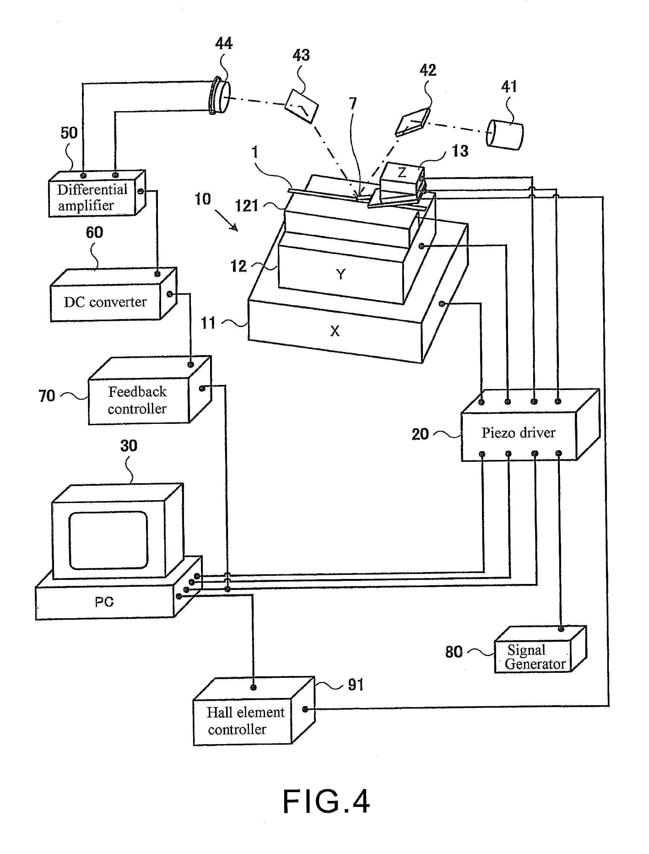
[0015] FIG. 4 is a schematic of a magnetic head inspection device in another aspect of the present invention.
[0016] FIG. 5 is a schematic illustrating the inspection method of the magnetic head inspection device in FIG. 4 and is a schematic view illustrating an enlarged construction of a magnetic head portion.
DESCRIPTION OF THE EMBODIMENTS
[0017] Reference will now be made in detail to the present embodiments of the invention, examples of which are illustrated in the accompanying drawings. Wherever possible, the same reference numbers are used in the drawings and the description to refer to the same or like parts.
[0018] FIG. 1 is a schematic illustrating the composition of a magnetic head inspection device in one aspect of the present invention. In the magnetic head inspection device in FIG. 1, the effective track width of an MR magnetic head, a giant magneto resistive (GMR) magnetic head, a tunnelling magneto resistive (TMR) magnetic head, and the like (referred to as an MR magnetic head below) can be measured in a rowbar state (a block formed by an arrangement of head sliders in block form) prior to the dicing process where the rowbar is separated into individual sliders (or chips).
[0019] Generally, the rowbar is a long and thin block of around 3 cm to 5 cm sliced from a wafer. One rowbar is composed of around 40 to 60 head sliders. In this embodiment of the magnetic head inspection device, the prescribed inspection is performed on the rowbar 1 as a work piece. Generally, the rowbars are provided in a tray with around 20 to 30 rowbars 1 are arranged side by side at a fixed spacing in the direction of the minor axis. A handling robot (not shown) extracts the rowbars 1 one by one from the tray (not shown) and transports the rowbars onto an inspection stage 10. The rowbar 1 that has been transported and placed on the inspection stage 10 is inspected in the following manner.
[0020] The inspection stage 10 is formed by an X stage 11 and a Y stage 12 capable of enabling the rowbar 1 to move in X and Y directions. The rowbar 1 is positioned by making preliminary contact of a single side surface in the direction of the major axis therefore and the reference surface of the Y stage 12. A carrier portion 121 for scanning the rowbar 1 is located on top of the Y stage 12. A stepped portion approximately coinciding with the rowbar 1 in shape is located at one side on the upper edge of the carrier portion 121. The rowbar 1 is placed in position by pressing against each of the bottom surface and side surface of the stepped portion. The rear surface (opposite to that having connecting terminals for the magnetic head) of the rowbar 1 is pressed against the back surface of the stepped portion. The stepped portion has reference surfaces that are each parallel to or orthogonal to the moving direction of the X stage 11 (X axis) and the moving direction of the Z stage 13 (Z axis). Therefore, the rowbar 1 may be accurately positioned in the X and Z directions by placing the rowbar 1 against the bottom surface and the side surface of the stepped portion of the carrier portion 121.
[0021] Although not shown, a camera for measuring position offset is located above the Y stage 12. The Z stage 13 moves the cantilever portion 7 of the MFM in the Z direction. The X stage 11, the Y stage 12, and the Z stage 13 of the inspection stage 10 are each composed of piezo stages. When the positioning is finished, suction holds the rowbar 1 on the carrier portion 121, and the front of a probe card (not shown) contacts the terminals at the front surface of the rowbar 1. Thereby, the write pole of a magnetic head in the rowbar 1 can be energized through its recording head coil.
[0022] A piezo driver 20 performs drive control of the X stage 11, the Y stage 12, and the Z stage 13 (the piezo stages) of the inspection stage 10. The control portion 30 comprising of a control computer that takes the form of a personal computer (PC) including a monitor as its basic configuration. As shown in the figure, the cantilever portion 7 having a sharp magnetic probe at its free end is located at a position above and pointing towards the rowbar 1 carried on the Y stage 12 of the inspection stage 10. The cantilever portion 7 is installed on an oscillator mounted below the Z stage 13. The oscillator comprising of a piezo element with an alternating current (AC) voltage applied at a frequency close to its mechanical resonance frequency via the piezo driver 20, that causes it to vibrate the magnetic probe up and down.
[0023] A displacement detection portion comprising of a semiconductor laser element 41, reflecting mirrors 42 and 43, and a displacement sensor 44. The displacement sensor 44 comprising of a dual-photo detector element. Light emitted from the semiconductor laser element 41 impinges onto the cantilever portion 7 after being deflected there by the reflecting mirror 42. Light reflected by the cantilever portion 7 is directed into the displacement sensor 44 by the reflecting mirror 43. A differential amplifier 50 implements a specific operation on the differential signal of the two signals output from the displacement sensor 44, and outputs its signal to a direct current (DC) converter 60. That is, the differential amplifier 50 outputs a displacement signal corresponding to a difference between the two signals output from the displacement sensor 44 to the DC converter 60. The DC converter 60 comprising of a root mean squared value to direct current (RMS-DC) converter that converts the displacement signal output from the differential amplifier 50 into an effective DC signal value.
[0024] The displacement signal output from the differential amplifier 50 is a signal corresponding to a displacement of the cantilever portion 7. Due to the oscillation of the cantilever portion 7, the displacement signal becomes an AC signal. The signal output from the DC converter 60 is output to a feedback controller 70. The feedback controller 70 outputs the signal output from the DC converter 60 as a signal for monitoring the amplitude of oscillation of the cantilever portion 7 to the control portion 30, and outputs the signal output from the DC converter 60 as a control signal for the Z stage 13 for adjusting the amplitude of oscillation of the cantilever portion 7 to the piezo driver 20. The control portion 30 monitors the signal and controls the Z stage 13 of the piezo driver 20 according to a value of the signal, in order that an initial position of the cantilever portion 7 can be adjusted before the measurement starts. In this aspect, the magnetic head flying height of an HDD is set as the initial position of the cantilever portion 7. A signal generator 80 provides an oscillating signal for oscillation of the cantilever portion 7 via the piezo driver 20. The piezo driver 20 vibrates the cantilever portion 7 at the frequency of the oscillating signal from the signal generator 80.
[0025] FIG. 2(A) and 2(B) are schematic views illustrating an inspection manner of the magnetic head inspection device in FIG. 1, wherein FIG. 2(A) is a view illustrating an enlarged construction of a magnetic head portion, and FIG. 2(B) is a view illustrating an example of a displacement signal of the cantilever portion. As shown in FIGS. 1 and 2(A), the cantilever portion 7 is positioned by the Z stage 13, such that the front end portion of the magnetic probe of the cantilever portion 7 is at a height from the surface of a magnetic head in the rowbar 1 equivalent to the magnetic head flying height Hf. The cantilever portion 7 performs a scanning motion in the scanning direction 71 relative to the rowbar 1 (magnetic head). In this aspect, the rowbar 1 moves via the X stage 11 and the Y stage 12.
[0026] At this point, the write pole of the magnetic head is undergoing an AC excitation, and thus the cantilever portion 7 is displaced synchronously with the AC excitation. The displacement of the cantilever portion 7 is shown by the displacement signal in FIG. 2(B), and thus an effective track width of the magnetic head can be detected from the displacement signal. Furthermore, the actual pole width of the magnetic head may be measured by performing a normal inspection with the MFM instead of with the AC excitation on the write pole.
[0027] In this way, for a conventional MFM, although the actual pole width of the magnetic head can be detected, the effective track width of the write pole of the magnetic head can also be inspected through the AC excitation performed on the write pole of the magnetic head while at the same time through the scanning motion performed by the cantilever portion 7 at a flying height of the magnetic head, thereby achieving inspection of the write track width of the magnetic head in the earliest possible phase of the manufacturing process, as shown in this implementation aspect.
[0028] FIG. 3 is a flow chart illustrating an example of a magnetic head manufacturing process including an inspection process of the write pole using an MFM of the present invention. Referring to the figure, in the wafer process, film deposition, etching, cleaning, and other semiconductor like processes are performed. In the rowbar process, a bar-shaped rowbar is sliced from a wafer, and lapping, air bearing surface (ABS) formation, cleaning, carbon protective film deposition, and other processes are performed on the rowbar. In the write pole test process, the effective track width of the write pole is measured for the bar-shaped rowbar using the MFM in FIG. 1. In the read element test process, similarly, electromagnetic conversion characteristics of each read element are measured within the bar-shaped rowbar. In the slider process, the bar-shaped rowbar is divided up (diced) and each slider is machined into a chip shape, a cleaning and an inspection process are performed. In the HGA process, a magnetic head slider already machined into the chip shape is connected to a suspension, and a cleaning process and an inspection process are performed. Afterwards, the HDD processes (head stack assembly (HSA) process and head disk assembly (HDA) process) (not shown) are performed. According to this embodiment, a good-or-bad determination may be performed on the effective track width of the write pole in the rowbar shape, thereby improving the productivity and enabling early feedback on previous processes.
[0029] FIG. 4 is a schematic view illustrating the construction of another embodiment of a magnetic head inspection device in an implementation aspect of the present invention. In FIG. 4, like symbols are used to indicate parts having the same constitution as those in FIG. 1, and thus descriptions thereof are omitted. FIG. 5 is a schematic view illustrating an inspection manner of the magnetic head inspection device in FIG. 4 and is a schematic view illustrating an enlarged construction of a magnetic head portion. The difference between the magnetic head inspection device in FIGS. 4 and 5 and that in FIGS. 1 and 2 lies in that, a Hall element 90 is mounted on the cantilever portion 7, and the shape of the magnetic field (an absolute value of the magnetic field) generated by the magnetic head is directly measured, so that an effective magnetic track width can be measured. That is, the magnetic head inspection device in FIG. 4 is characterized in an SHPM (Scanning Hall Probe Microscope) that makes the Hall element 90 infinitely close to the magnetic material to be observed so as to detect and visualize the magnetic field. The Hall element 90 is formed by patterning a GaAs/AlGaAs epitaxial wafer through photolithography. A Hall element controller 91 provides a current to terminals of the Hall element 90. The Hall element controller 91 adopts a nanovolt meter or other meters to measure the Hall voltage generated between the other terminals of the Hall element 90, and outputs the measured Hall voltage to the control portion 30. A PC of the control portion 30 makes a two-dimensional distribution of surface magnetic field emission according to the Hall voltage, and measures the effective track width of the magnetic head according to the two-dimensional distribution.
[0030] Instead of the Hall element 90 being installed on the cantilever portion 7 of the magnetic head inspection device in FIGS. 4 and 5, an MR sensor element may also be installed at the front end portion of the cantilever portion 7, so as to apply an SMRM (Scanning Magneto-Resistance Microscope) in the aforementioned magnetism measurement. At this point, an MR sensor controller may be used to replace the Hall element controller to cope with the above situation. In this manner, the Hall element or MR element can be installed on the cantilever portion 7 of the MFM, so that SHPM or SMRM is capable of implementing the shape measurement and magnetism measurement (measurement of the effective track width) of the write pole at the same time.
[0031] It will be apparent to those skilled in the art that various modifications and variations can be made to the structure of the present invention without departing from the scope or spirit of the invention. In view of the foregoing, it is intended that the present invention cover modifications and variations of this invention provided they fall within the scope of the following claims and their equivalents.
* * * * *
D00000
D00001
D00002
D00003
D00004
D00005
XML
uspto.report is an independent third-party trademark research tool that is not affiliated, endorsed, or sponsored by the United States Patent and Trademark Office (USPTO) or any other governmental organization. The information provided by uspto.report is based on publicly available data at the time of writing and is intended for informational purposes only.
While we strive to provide accurate and up-to-date information, we do not guarantee the accuracy, completeness, reliability, or suitability of the information displayed on this site. The use of this site is at your own risk. Any reliance you place on such information is therefore strictly at your own risk.
All official trademark data, including owner information, should be verified by visiting the official USPTO website at www.uspto.gov. This site is not intended to replace professional legal advice and should not be used as a substitute for consulting with a legal professional who is knowledgeable about trademark law.