Micro flow channel chip
Shinoda , et al. January 5, 2
U.S. patent number D907,242 [Application Number D/440,326] was granted by the patent office on 2021-01-05 for micro flow channel chip. This patent grant is currently assigned to SONY CORPORATION. The grantee listed for this patent is Sony Corporation. Invention is credited to Shoji Akiyama, Yuji Akiyama, Gakuji Hashimoto, Tatsumi Ito, Masaya Kakuta, Hiroto Kasai, Masataka Shinoda, Takeshi Yamasaki.


| United States Patent | D907,242 |
| Shinoda , et al. | January 5, 2021 |
Micro flow channel chip
Claims
CLAIM The ornamental design for a micro flow channel chip, as shown and described.
| Inventors: | Shinoda; Masataka (Tokyo, JP), Akiyama; Shoji (Tokyo, JP), Kakuta; Masaya (Tokyo, JP), Yamasaki; Takeshi (Tokyo, JP), Ito; Tatsumi (Tokyo, JP), Akiyama; Yuji (Tokyo, JP), Hashimoto; Gakuji (Tokyo, JP), Kasai; Hiroto (Tokyo, JP) | ||||||||||
|---|---|---|---|---|---|---|---|---|---|---|---|
| Applicant: |
|
||||||||||
| Assignee: | SONY CORPORATION (Tokyo,
JP) |
||||||||||
| Appl. No.: | D/440,326 | ||||||||||
| Filed: | December 20, 2012 |
Related U.S. Patent Documents
| Application Number | Filing Date | Patent Number | Issue Date | ||
|---|---|---|---|---|---|
| 29371150 | Oct 29, 2010 | D673286 | |||
| 29371203 | Nov 24, 2010 | D673287 | |||
| 29421304 | Jun 29, 2012 | D704580 | |||
Foreign Application Priority Data
| Apr 29, 2010 [JP] | D2010-010817 | |||
| Apr 29, 2010 [JP] | D2010-010818 | |||
| Apr 29, 2010 [JP] | D2010-010819 | |||
| Apr 29, 2010 [JP] | D2010-010820 | |||
| Apr 29, 2010 [JP] | D2010-010821 | |||
| Apr 29, 2010 [JP] | D2010-010822 | |||
| Apr 29, 2010 [JP] | D2010-010823 | |||
| Apr 29, 2010 [JP] | D2010-010824 | |||
| Apr 29, 2010 [JP] | D2010-010825 | |||
| Apr 29, 2010 [JP] | D2010-010826 | |||
| Jul 28, 2010 [JP] | D2010-018425 | |||
| Jul 28, 2010 [JP] | D2010-018426 | |||
| Jul 28, 2010 [JP] | D2010-018427 | |||
| Mar 8, 2012 [JP] | D2012-005307 | |||
| Mar 8, 2012 [JP] | D2012-005308 | |||
| Mar 8, 2012 [JP] | D2012-005309 | |||
| Mar 8, 2012 [JP] | D2012-005310 | |||
| Current U.S. Class: | D24/225; D24/216 |
| Current International Class: | 2401 |
| Field of Search: | ;D24/216,223,224,225,226 ;D10/81 ;422/500,547 ;435/287.1 |
References Cited [Referenced By]
U.S. Patent Documents
| 4732479 | March 1988 | Tanaka |
| 5370842 | December 1994 | Miyazaki |
| D375799 | November 1996 | Leiva et al. |
| 6210986 | April 2001 | Arnold |
| 6561208 | May 2003 | O'Connor |
| 6773567 | August 2004 | Wolk |
| 7708949 | May 2010 | Stone et al. |
| 7740804 | June 2010 | Samsoondar |
| 7757568 | July 2010 | Shiraki |
| D636891 | April 2011 | Nicholls et al. |
| D636892 | April 2011 | Nicholls et al. |
| D636893 | April 2011 | Nicholls et al. |
| 8101137 | January 2012 | Polwart et al. |
| D673286 | December 2012 | Shinoda |
| D795724 | August 2017 | Akiyama |
| 2002/0048256 | April 2002 | Yamasaki |
| 2003/0141003 | July 2003 | Yamasaki |
| 2004/0027703 | February 2004 | Yamasaki |
| 2005/0118062 | June 2005 | Otake |
| 2005/0161326 | July 2005 | Morita |
| 2005/0183496 | August 2005 | Baek |
| 2005/0214173 | September 2005 | Facer |
| 2006/0034728 | February 2006 | Kloepfer |
| 2006/0040297 | February 2006 | Leamon |
| 2006/0147343 | July 2006 | Teramoto |
| 2006/0228254 | October 2006 | Kusaka et al. |
| 2008/0026369 | January 2008 | Dual et al. |
| 2008/0148822 | June 2008 | Phelan |
| 2008/0248582 | October 2008 | Wyatt |
| 2009/0114285 | May 2009 | Hashimoto et al. |
| 2009/0148348 | June 2009 | Pettigrew et al. |
| 2009/0149345 | June 2009 | Nishi |
| 2009/0253181 | October 2009 | Vangbo |
| 2010/0258211 | October 2010 | Burns |
| 2010/0317094 | December 2010 | Ricco et al. |
| 2011/0020855 | January 2011 | Shinoda |
| 2011/0045577 | February 2011 | Bruzewicz |
| 2011/0076735 | March 2011 | Jovanovich et al. |
| 2011/0104817 | May 2011 | Kang |
| 2011/0151578 | June 2011 | Abate |
| 2013/0070243 | March 2013 | Goehde |
| 2013/0217106 | August 2013 | Jones |
| 2017/0122902 | May 2017 | Tominaga |
| D1269428 | Apr 2006 | JP | |||
| 2010-54492 | Mar 2010 | JP | |||
| D1383781 | Mar 2010 | JP | |||
Attorney, Agent or Firm: Michael Best and Friedrich LLP
Description
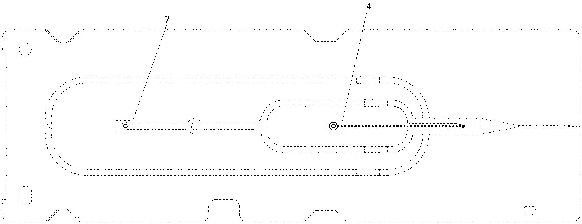
FIG. 1 is a top plan view of a micro flow channel chip showing our new design, a bottom plan view thereof being a mirror image;
FIG. 2 is a front elevational view thereof, a rear elevational view being a mirror image;
FIG. 3 is a right side elevational view thereof, a left side elevational view being a mirror image;
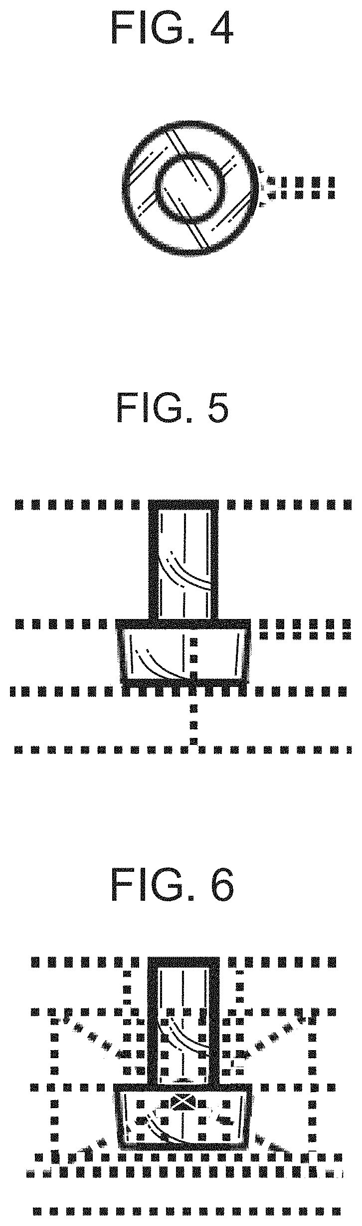
FIG. 4 is a partially enlarged top plan view thereof within the area designated as 4 of FIG. 1;
FIG. 5 is a partially enlarged front elevational view thereof within the area designated as 5 of FIG. 2;
FIG. 6 is a partially enlarged right side elevational view thereof within the area designated as 6 of FIG. 3;
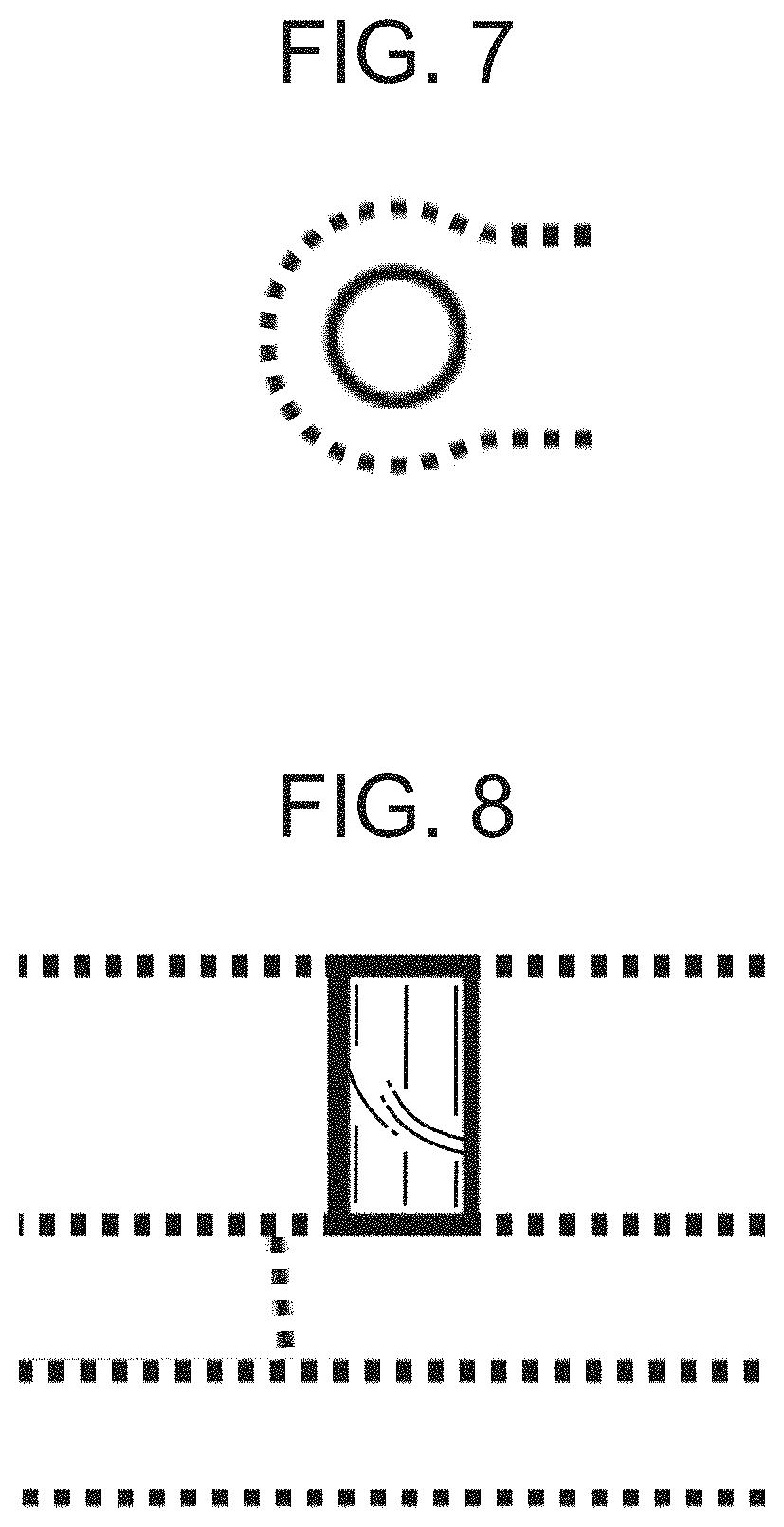
FIG. 7 is a partially enlarged top plan view thereof within the area designated as 7 of FIG. 1; and,
FIG. 8 is a partially enlarged front elevational view thereof within the area designated as 8 of FIG. 2.
The broken lines illustrating unclaimed portions of the micro flow channel chip form no part of the claimed design.
* * * * *
D00000
D00001
D00002
D00003
D00004
XML
uspto.report is an independent third-party trademark research tool that is not affiliated, endorsed, or sponsored by the United States Patent and Trademark Office (USPTO) or any other governmental organization. The information provided by uspto.report is based on publicly available data at the time of writing and is intended for informational purposes only.
While we strive to provide accurate and up-to-date information, we do not guarantee the accuracy, completeness, reliability, or suitability of the information displayed on this site. The use of this site is at your own risk. Any reliance you place on such information is therefore strictly at your own risk.
All official trademark data, including owner information, should be verified by visiting the official USPTO website at www.uspto.gov. This site is not intended to replace professional legal advice and should not be used as a substitute for consulting with a legal professional who is knowledgeable about trademark law.