Electronic device
Park , et al.
U.S. patent number D890,111 [Application Number D/676,966] was granted by the patent office on 2020-07-14 for electronic device. This patent grant is currently assigned to Samsung Electronics Co., Ltd.. The grantee listed for this patent is Samsung Electronics Co., Ltd.. Invention is credited to Chang Sin Cho, Seung Ho Jang, Dong Kyun Kim, Hyoung Shin Park, Seon Keun Park.


View All Diagrams
| United States Patent | D890,111 |
| Park , et al. | July 14, 2020 |
Electronic device
Claims
CLAIM We claim the ornamental design for an electronic device, as shown and described.
| Inventors: | Park; Hyoung Shin (Suwon-si, KR), Jang; Seung Ho (Suwon-si, KR), Kim; Dong Kyun (Suwon-si, KR), Park; Seon Keun (Suwon-si, KR), Cho; Chang Sin (Suwon-si, KR) | ||||||||||
|---|---|---|---|---|---|---|---|---|---|---|---|
| Applicant: |
|
||||||||||
| Assignee: | Samsung Electronics Co., Ltd.
(Suwon-si, KR) |
||||||||||
| Appl. No.: | D/676,966 | ||||||||||
| Filed: | January 16, 2019 |
Foreign Application Priority Data
| Jul 23, 2018 [KR] | 30-2018-0033899 | |||
| Jul 23, 2018 [KR] | 30-2018-0033900 | |||
| Current U.S. Class: | D14/138G |
| Current International Class: | 1403 |
| Field of Search: | ;D14/138G,248,341,371,374,138R,138AA,138AB,138AC,138AD,138C,247 |
References Cited [Referenced By]
U.S. Patent Documents
| D548218 | August 2007 | Hong |
| D555616 | November 2007 | Lin |
| D558726 | January 2008 | Wang |
| D577704 | September 2008 | Park |
| D584708 | January 2009 | Wu |
| D585416 | January 2009 | Kim |
| D589487 | March 2009 | Park |
| D607429 | January 2010 | Lim |
| D616852 | June 2010 | Kim |
| D620469 | July 2010 | Chang |
| D656477 | March 2012 | Yi |
| D686586 | July 2013 | Cho |
| D694730 | December 2013 | Lee |
| D695255 | December 2013 | Kim |
| D700164 | February 2014 | Park |
| D783565 | April 2017 | Kim |
| D783566 | April 2017 | Kim |
| D803176 | November 2017 | Cho |
| D807851 | January 2018 | Cho |
| D807853 | January 2018 | Oh |
| D813186 | March 2018 | Lee |
| D815080 | April 2018 | Cho |
| D831605 | October 2018 | Baik |
| D839848 | February 2019 | Baik |
| D847776 | May 2019 | Ryu |
| D849706 | May 2019 | Park |
| D854508 | July 2019 | Park |
| D856958 | August 2019 | Seo |
| D857643 | August 2019 | Choi |
| D860152 | September 2019 | Cho |
| D861630 | October 2019 | Chiang |
| D865732 | November 2019 | Park |
| D865733 | November 2019 | Park |
| D865734 | November 2019 | Park |
| D865735 | November 2019 | Park |
| D865737 | November 2019 | Park |
| D865738 | November 2019 | Park |
| D866496 | November 2019 | Kim |
| D866540 | November 2019 | Park |
| D866541 | November 2019 | Park |
| D866542 | November 2019 | Park |
| D867317 | November 2019 | Ha |
| D867351 | November 2019 | Park |
| D871360 | December 2019 | Seo |
| D872703 | January 2020 | Seo |
| 10530911 | January 2020 | Bao |
| D875701 | February 2020 | Park |
| D876383 | February 2020 | Park |
| D876384 | February 2020 | Park |
| 2018/0196475 | July 2018 | Bao |
| 2019/0305403 | October 2019 | Wang |
| 2019/0312964 | October 2019 | Haiberger |
Other References
|
Samsung Galaxy S10 5G, announced Feb. 2019, [online], [retrieved on May 22, 2019]. Retrieved from Internet ,<URL: http://www.gsmarena.com>. cited by examiner . Samsung Galaxy S10+, announced Feb. 2019, [online], [retrieved on May 22, 2019]. Retrieved from Internet ,<URL: http://www.gsmarena.com>. cited by examiner . Samsung Galaxy S10e, announced Feb. 2019, [online], [retrieved on May 22, 2019]. Retrieved from Internet ,<URL: http://www.gsmarena.com>. cited by examiner . Nokia X71, announced Apr. 2019, [online], [retrieved on May 22, 2019]. Retrieved from Internet ,<URL: http://www.gsmarena.com>. cited by examiner . Motorola One Vision, announced May 2019, [online], [retrieved on May 22, 2019]. Retrieved from Internet ,<URL: http://www.gsmarena.com>. cited by examiner . Honor 20, announced May 2019, [online], [retrieved on May 22, 2019]. Retrieved from Internet ,<URL: http://www.gsmarena.com>. cited by examiner. |
Primary Examiner: Eland; Bridget L
Attorney, Agent or Firm: NSIP Law
Description
FIG. 1 is a front perspective view of an electronic device showing our new design according to a first embodiment;
FIG. 2 is a front view thereof;
FIG. 3 is a rear view thereof;
FIG. 4 is a left-side view thereof;
FIG. 5 is a right-side view thereof;
FIG. 6 is a top view thereof;
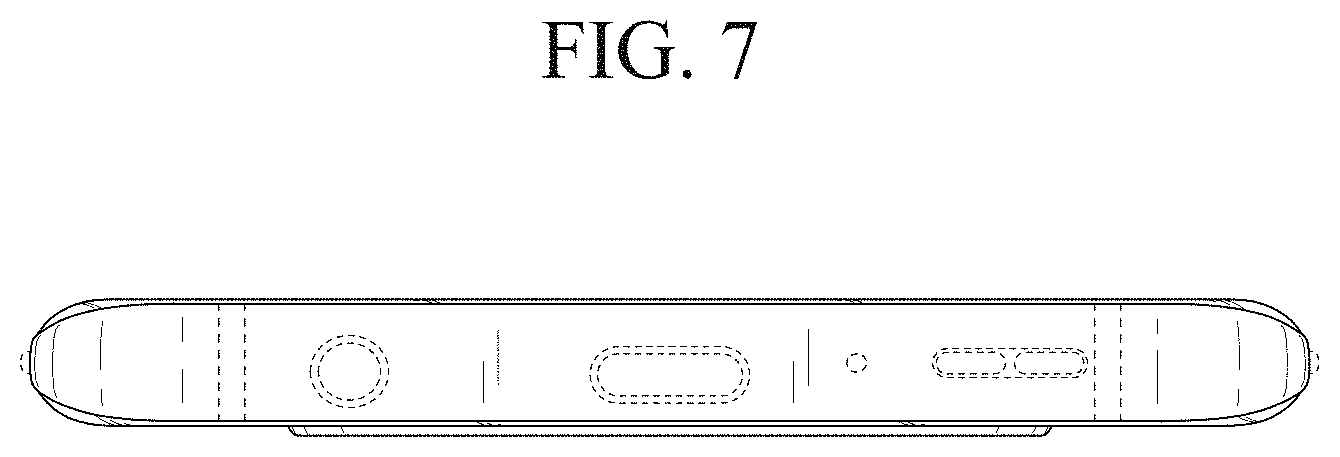
FIG. 7 is a bottom view thereof;
FIG. 8 is a rear perspective view thereof;
FIG. 9 is a front perspective view of an electronic device showing our new design according to a second embodiment;
FIG. 10 is a front view thereof;
FIG. 11 is a rear view thereof;
FIG. 12 is a left-side view thereof;
FIG. 13 is a right-side view thereof;
FIG. 14 is a top plan view thereof;
FIG. 15 is a bottom plan view thereof;
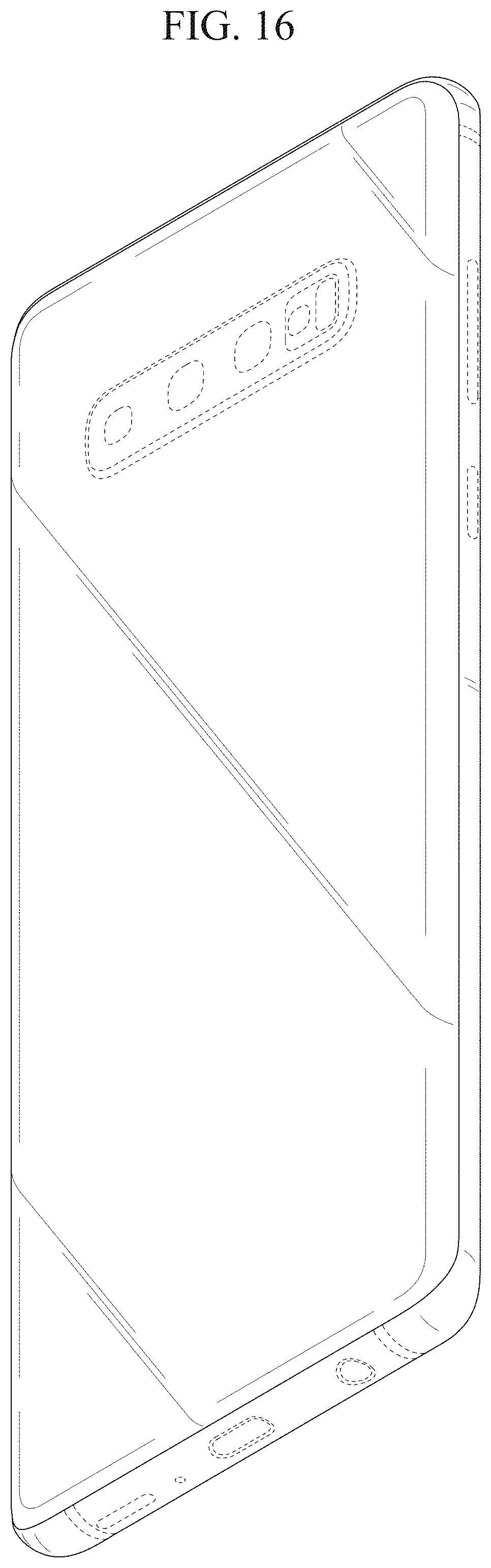
FIG. 16 is a rear perspective view thereof;
FIG. 17 is a front perspective view of an electronic device showing our new design according to a third embodiment;
FIG. 18 is a front view thereof;
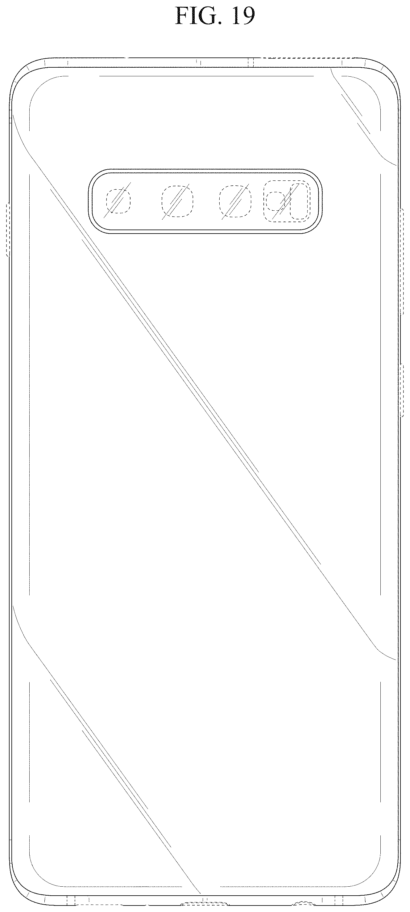
FIG. 19 is a rear view thereof;
FIG. 20 is a left-side view thereof;
FIG. 21 is a right-side view thereof;
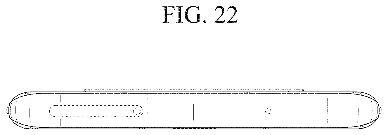
FIG. 22 is a top plan view thereof;
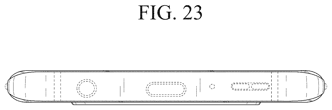
FIG. 23 is a bottom plan view thereof;
FIG. 24 is a rear perspective view thereof;
FIG. 25 is a front perspective view of an electronic device showing our new design according to a fourth embodiment;
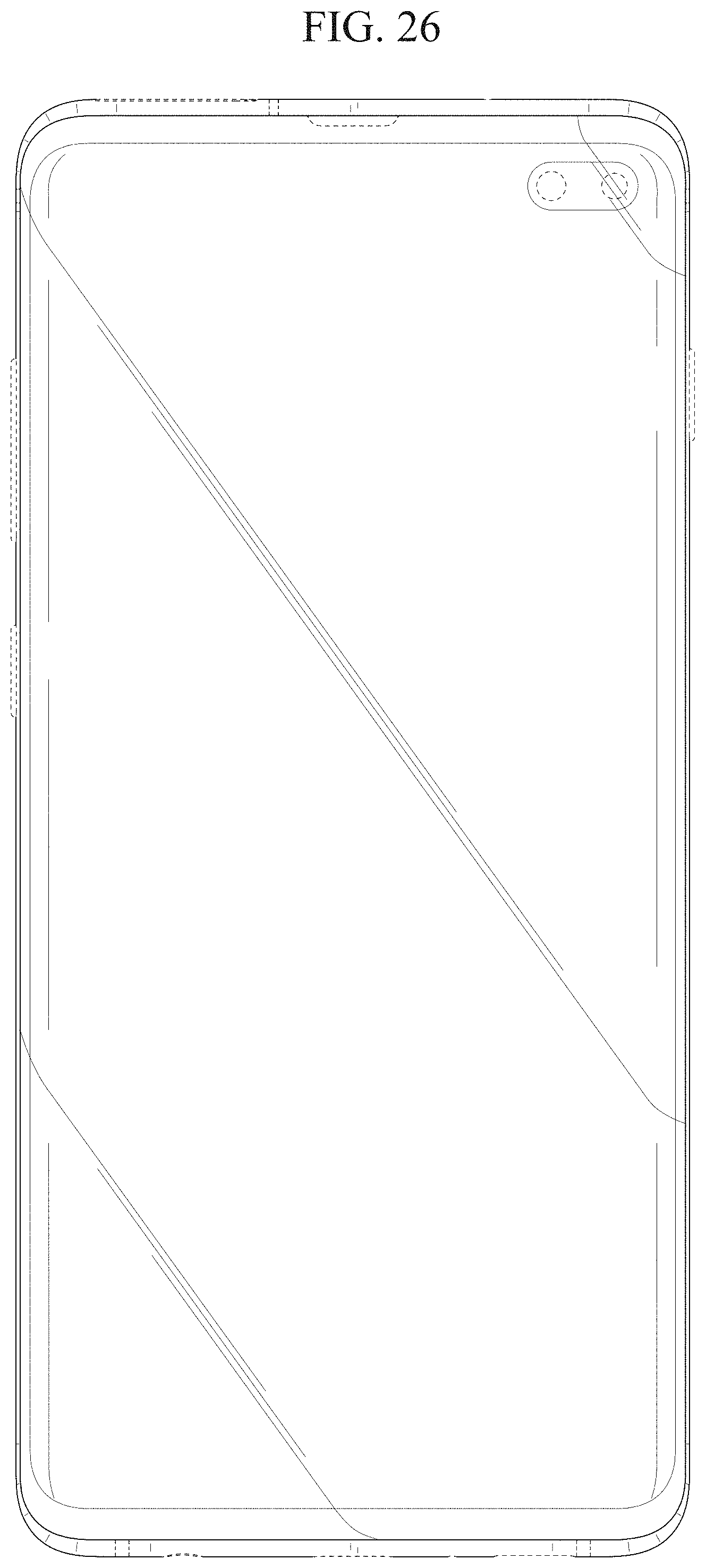
FIG. 26 is a front view thereof;
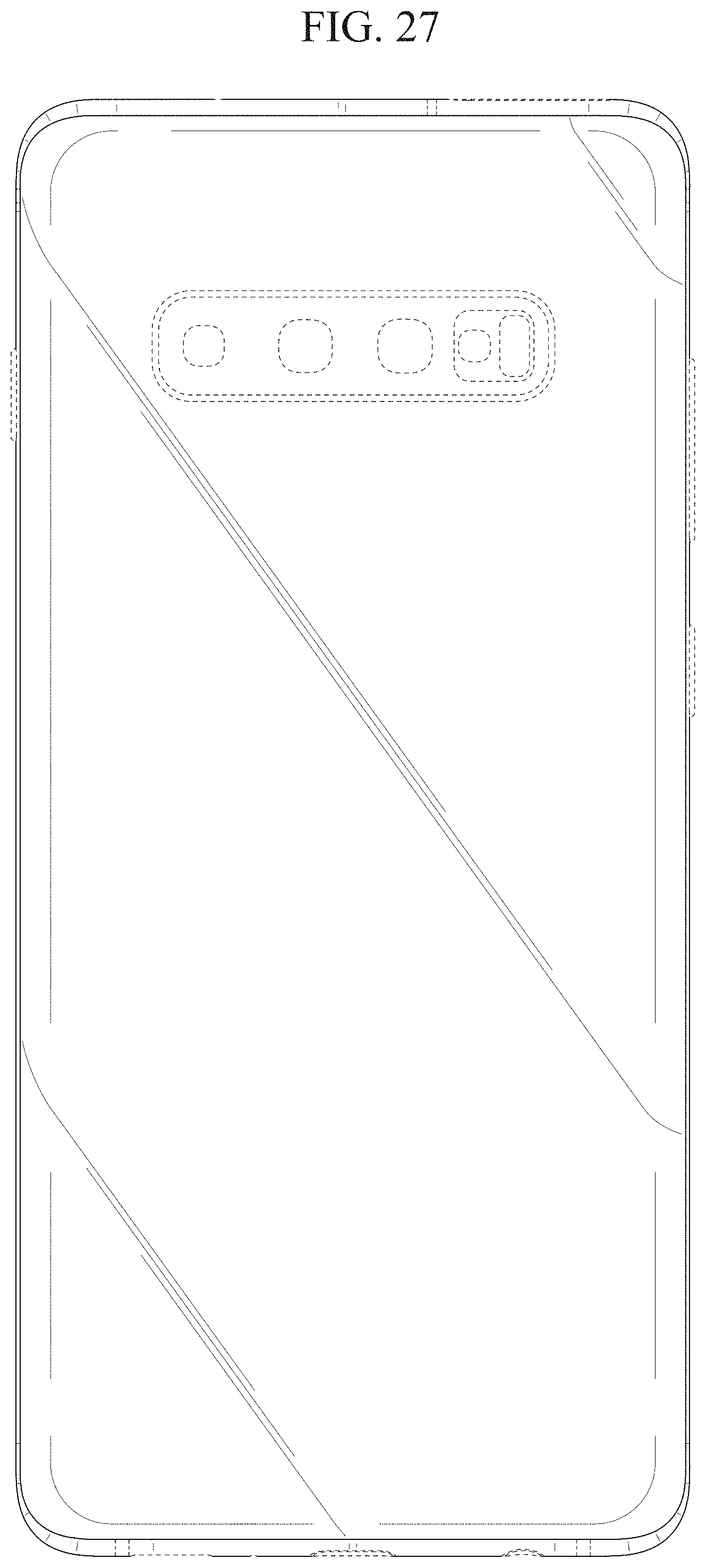
FIG. 27 is a rear view thereof;
FIG. 28 is a left-side view thereof;
FIG. 29 is a right-side view thereof;
FIG. 30 is a top plan view thereof;
FIG. 31 is a bottom plan view thereof;
FIG. 32 is a rear perspective view thereof;
FIG. 33 is a front view of an electronic device showing our new design according to a fifth embodiment;
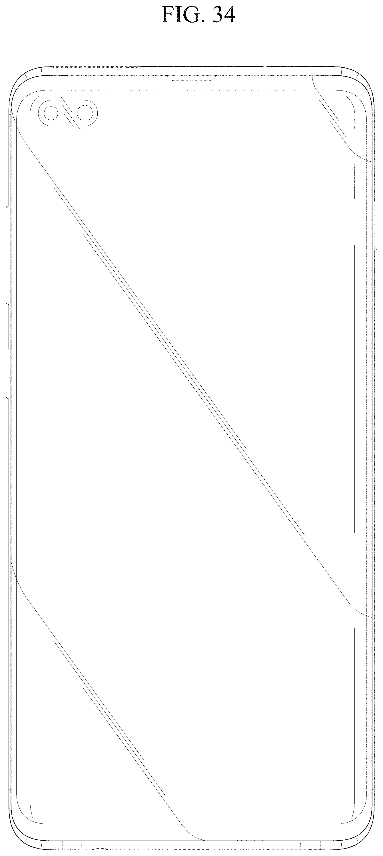
FIG. 34 is a front view of an electronic device showing our new design according to a sixth embodiment;
FIG. 35 is a front view of an electronic device showing our new design according to a seventh embodiment;
FIG. 36 is a front view of an electronic device showing our new design according to an eighth embodiment;
FIG. 37 is a front view of an electronic device showing our new design according to a ninth embodiment;
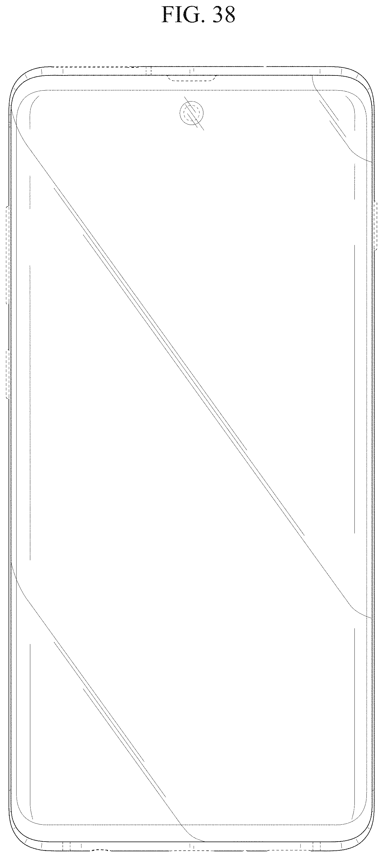
FIG. 38 is a front view of an electronic device showing our new design according to a tenth embodiment;
FIG. 39 is a front view of an electronic device showing our new design according to an eleventh embodiment;
FIG. 40 is a front view of an electronic device showing our new design according to a twelfth embodiment;
FIG. 41 is a front perspective view of an electronic device showing our new design according to a thirteenth embodiment;
FIG. 42 is a front view thereof;
FIG. 43 is a rear view thereof;
FIG. 44 is a left-side view thereof;
FIG. 45 is a right-side view thereof;
FIG. 46 is a top plan view thereof;
FIG. 47 is a bottom plan view thereof;
FIG. 48 is a rear perspective view thereof;
FIG. 49 is a front perspective view of an electronic device showing our new design according to a fourteenth embodiment;
FIG. 50 is a front view thereof;
FIG. 51 is a rear view thereof;
FIG. 52 is a left-side view thereof;
FIG. 53 is a right-side view thereof;
FIG. 54 is a top plan view thereof;
FIG. 55 is a bottom plan view thereof; and,
FIG. 56 is a rear perspective view thereof.
The evenly-dashed broken lines in the figures depict portions of the electronic device which form no part of the claimed design.
The dot-dash broken lines in the figures represent boundaries of the claimed design and form no part thereof. The appearance of any portion of the article between the evenly-spaced pairs of dot-dash broken lines forms no part of the claimed design.
The rear, left-side, right-side, top, bottom and rear perspective views of the fifth through twelfth embodiments of the electronic device depicted in FIGS. 33 through 40 have been omitted because they are exact duplicates of the same views of the electronic device design that are depicted in FIGS. 11 through 16.
* * * * *
References
D00000
D00001
D00002
D00003
D00004
D00005
D00006
D00007
D00008
D00009
D00010
D00011
D00012

D00013

D00014

D00015

D00016
D00017

D00018

D00019
D00020

D00021

D00022
D00023
D00024

D00025

D00026
D00027
D00028

D00029

D00030

D00031

D00032

D00033

D00034
D00035

D00036

D00037

D00038
D00039

D00040

D00041

D00042

D00043

D00044

D00045

D00046

D00047

D00048

D00049

D00050

D00051

D00052

D00053

D00054

D00055

D00056

XML
uspto.report is an independent third-party trademark research tool that is not affiliated, endorsed, or sponsored by the United States Patent and Trademark Office (USPTO) or any other governmental organization. The information provided by uspto.report is based on publicly available data at the time of writing and is intended for informational purposes only.
While we strive to provide accurate and up-to-date information, we do not guarantee the accuracy, completeness, reliability, or suitability of the information displayed on this site. The use of this site is at your own risk. Any reliance you place on such information is therefore strictly at your own risk.
All official trademark data, including owner information, should be verified by visiting the official USPTO website at www.uspto.gov. This site is not intended to replace professional legal advice and should not be used as a substitute for consulting with a legal professional who is knowledgeable about trademark law.