Double dual slot load lock chamber
Kurita , et al. December 31, 2
U.S. patent number 8,616,820 [Application Number 11/926,720] was granted by the patent office on 2013-12-31 for double dual slot load lock chamber. This patent grant is currently assigned to Applied Materials, Inc.. The grantee listed for this patent is Wendell T. Blonigan, Shinichi Kurita. Invention is credited to Wendell T. Blonigan, Shinichi Kurita.


| United States Patent | 8,616,820 |
| Kurita , et al. | December 31, 2013 |
Double dual slot load lock chamber
Abstract
Provided herein is a double dual slot load lock chamber. The double dual slot load lock chamber includes two isolated load lock regions that are vertically stacked and share a common wall, wherein each isolated load lock region comprises two substrate slots.
| Inventors: | Kurita; Shinichi (San Jose, CA), Blonigan; Wendell T. (Union City, CA) | ||||||||||
|---|---|---|---|---|---|---|---|---|---|---|---|
| Applicant: |
|
||||||||||
| Assignee: | Applied Materials, Inc. (Santa
Clara, CA) |
||||||||||
| Family ID: | 36815823 | ||||||||||
| Appl. No.: | 11/926,720 | ||||||||||
| Filed: | October 29, 2007 |
Prior Publication Data
| Document Identifier | Publication Date | |
|---|---|---|
| US 20080044259 A1 | Feb 21, 2008 | |
Related U.S. Patent Documents
| Application Number | Filing Date | Patent Number | Issue Date | ||
|---|---|---|---|---|---|
| 11278318 | Mar 31, 2006 | 7316966 | |||
| 09957784 | Sep 21, 2001 | 7105463 | |||
| Current U.S. Class: | 414/217; 414/217.1; 414/221; 414/939 |
| Current CPC Class: | H01L 21/67748 (20130101); H01L 21/67201 (20130101); H01L 21/67196 (20130101) |
| Current International Class: | H01L 21/00 (20060101); H01L 21/677 (20060101); B65G 47/90 (20060101); H01L 21/67 (20060101) |
| Field of Search: | ;414/217,416,331,939,217.1,221 ;118/71,719 ;204/298.25 |
References Cited [Referenced By]
U.S. Patent Documents
| 3976330 | August 1976 | Babinski et al. |
| 4047624 | September 1977 | Dorenbos |
| 4178113 | December 1979 | Beaver, II et al. |
| 4311542 | January 1982 | Mueller et al. |
| 4512391 | April 1985 | Harra |
| 4680061 | July 1987 | Lamont, Jr. |
| 4687542 | August 1987 | Davis et al. |
| 4693777 | September 1987 | Hazano et al. |
| 4709655 | December 1987 | Van Mastrigt |
| 4759681 | July 1988 | Nogami |
| 4770590 | September 1988 | Hugues et al. |
| 4775281 | October 1988 | Prentakis |
| 4785962 | November 1988 | Toshima |
| 4801241 | January 1989 | Zajac et al. |
| 4816098 | March 1989 | Davis et al. |
| 4828224 | May 1989 | Crabb et al. |
| 4836733 | June 1989 | Hertel et al. |
| 4846102 | July 1989 | Ozias |
| 4857689 | August 1989 | Lee |
| 4863547 | September 1989 | Shidahara et al. |
| 4870923 | October 1989 | Sugimoto |
| 4895107 | January 1990 | Yano et al. |
| 4911103 | March 1990 | Davis et al. |
| 4913929 | April 1990 | Moslehi et al. |
| 4917556 | April 1990 | Stark et al. |
| 4923584 | May 1990 | Bramhall, Jr. et al. |
| 4951601 | August 1990 | Mayden et al. |
| 4952299 | August 1990 | Chrisos et al. |
| 4966519 | October 1990 | Davis et al. |
| 4989543 | February 1991 | Schmitt |
| 4990047 | February 1991 | Wagner et al. |
| 5001327 | March 1991 | Hirasawa et al. |
| 5044871 | September 1991 | Davis et al. |
| 5060354 | October 1991 | Chizinsky |
| 5131460 | July 1992 | Krueger |
| 5186718 | February 1993 | Tepman et al. |
| 5187115 | February 1993 | Coleman |
| 5199483 | April 1993 | Bahng |
| 5202716 | April 1993 | Tateyama et al. |
| 5224809 | July 1993 | Maydan et al. |
| 5227708 | July 1993 | Lowrance |
| 5248370 | September 1993 | Tsui et al. |
| 5252807 | October 1993 | Chizinsky |
| 5254170 | October 1993 | Devilbiss et al. |
| 5259881 | November 1993 | Edwards et al. |
| 5259883 | November 1993 | Yamabe et al. |
| 5261935 | November 1993 | Ishii et al. |
| 5288379 | February 1994 | Namiki et al. |
| 5292393 | March 1994 | Maydan et al. |
| 5352294 | October 1994 | White et al. |
| 5355066 | October 1994 | Lowrance |
| 5376212 | December 1994 | Saiki |
| 5404894 | April 1995 | Shiraiwa |
| 5421889 | June 1995 | Pollock et al. |
| 5443346 | August 1995 | Murata et al. |
| 5445484 | August 1995 | Kato et al. |
| 5447409 | September 1995 | Grunes et al. |
| 5464313 | November 1995 | Ohsawa |
| 5469035 | November 1995 | Lowrance |
| 5470784 | November 1995 | Coleman |
| 5474410 | December 1995 | Ozawa et al. |
| 5512320 | April 1996 | Turner et al. |
| 5516732 | May 1996 | Flegal |
| 5536128 | July 1996 | Shimoyashiro et al. |
| 5562383 | October 1996 | Iwai et al. |
| 5570994 | November 1996 | Somekh et al. |
| 5586585 | December 1996 | Bonora et al. |
| 5588827 | December 1996 | Muka |
| 5607009 | March 1997 | Turner et al. |
| 5609689 | March 1997 | Kato et al. |
| 5611655 | March 1997 | Fukasawa et al. |
| 5611865 | March 1997 | White et al. |
| 5615988 | April 1997 | Wiesler et al. |
| 5616208 | April 1997 | Lee |
| 5636964 | June 1997 | Somekh et al. |
| 5655277 | August 1997 | Galdos et al. |
| 5674786 | October 1997 | Turner et al. |
| 5685684 | November 1997 | Kato et al. |
| 5695568 | December 1997 | Sinha et al. |
| 5697749 | December 1997 | Iwabuchi et al. |
| 5700127 | December 1997 | Harada et al. |
| 5716207 | February 1998 | Mishina et al. |
| 5738767 | April 1998 | Coad et al. |
| 5751003 | May 1998 | Rose et al. |
| 5784799 | July 1998 | Kato et al. |
| 5795355 | August 1998 | Moran |
| 5820679 | October 1998 | Yokoyama et al. |
| 5855681 | January 1999 | Maydan et al. |
| 5855726 | January 1999 | Soraoka et al. |
| 5882165 | March 1999 | Maydan et al. |
| 5884009 | March 1999 | Okase |
| 5891251 | April 1999 | MacLeish et al. |
| 5902088 | May 1999 | Fairbairn et al. |
| 5909994 | June 1999 | Blum et al. |
| 5913978 | June 1999 | Kato et al. |
| 5933426 | August 1999 | Motoori |
| 5934856 | August 1999 | Asakawa et al. |
| 5937541 | August 1999 | Weigand et al. |
| 5942013 | August 1999 | Akimoto |
| 5944857 | August 1999 | Edwards et al. |
| 5951770 | September 1999 | Perlov et al. |
| 5954472 | September 1999 | Hofmeister et al. |
| 5961269 | October 1999 | Kroeker |
| 5997235 | December 1999 | Hofmeister |
| 6007675 | December 1999 | Toshima |
| 6016611 | January 2000 | White et al. |
| 6034000 | March 2000 | Heyder et al. |
| 6039770 | March 2000 | Yang et al. |
| 6042623 | March 2000 | Edwards |
| 6044534 | April 2000 | Seo et al. |
| 6048154 | April 2000 | Wytman |
| 6059507 | May 2000 | Adams |
| 6079693 | June 2000 | Ettinger et al. |
| 6082950 | July 2000 | Altwood et al. |
| 6086362 | July 2000 | White et al. |
| 6106634 | August 2000 | Ghanayem et al. |
| 6143083 | November 2000 | Yonemitsu et al. |
| 6145673 | November 2000 | Burrows et al. |
| 6176668 | January 2001 | Kurita et al. |
| 6193507 | February 2001 | White et al. |
| 6206176 | March 2001 | Blonigan |
| 6213704 | April 2001 | White et al. |
| 6215897 | April 2001 | Beer et al. |
| 6224680 | May 2001 | Toshima |
| 6235634 | May 2001 | White et al. |
| 6254328 | July 2001 | Wytman |
| 6270582 | August 2001 | Rivkin et al. |
| 6286230 | September 2001 | White et al. |
| 6315512 | November 2001 | Tabrizi et al. |
| 6318945 | November 2001 | Hofmeister |
| 6338626 | January 2002 | Saeki |
| 6340405 | January 2002 | Park |
| 6382895 | May 2002 | Konishi et al. |
| 6410455 | June 2002 | Kuribayashi et al. |
| 6435868 | August 2002 | White et al. |
| 6450750 | September 2002 | Heyder et al. |
| 6486444 | November 2002 | Fairbairn et al. |
| 6503365 | January 2003 | Kim et al. |
| 6517303 | February 2003 | White et al. |
| 6558509 | May 2003 | Kraus et al. |
| 6568552 | May 2003 | Tabrizi et al. |
| 6568899 | May 2003 | Kuribayashi et al. |
| 6602797 | August 2003 | Kuribayashi et al. |
| 6609869 | August 2003 | Aggarwal et al. |
| 6610150 | August 2003 | Savage et al. |
| 6647665 | November 2003 | Tabrizi et al. |
| 6949143 | September 2005 | Kurita et al. |
| 7105463 | September 2006 | Kurita et al. |
| 2001/0041120 | November 2001 | Hofmeister |
| 2002/0034886 | March 2002 | Kurita et al. |
| 2002/0137346 | September 2002 | Donaldson et al. |
| 0 359 525 | Mar 1990 | EP | |||
| 0 607 797 | Jul 1994 | EP | |||
| 0 608 620 | Aug 1994 | EP | |||
| 0 608 633 | Aug 1994 | EP | |||
| 0 684 630 | Nov 1995 | EP | |||
| 0 756 316 | Jan 1997 | EP | |||
| 0 935 279 | Aug 1999 | EP | |||
| 64-028933 | Jan 1989 | JP | |||
| 02-152251 | Jun 1990 | JP | |||
| 03 136345 | Jun 1991 | JP | |||
| 03-274746 | Dec 1991 | JP | |||
| 04-098848 | Mar 1992 | JP | |||
| 04-240721 | Aug 1992 | JP | |||
| 05-013551 | Jan 1993 | JP | |||
| 05 179447 | Jul 1993 | JP | |||
| 05-283500 | Oct 1993 | JP | |||
| 06-104326 | Apr 1994 | JP | |||
| 06-156624 | Jun 1994 | JP | |||
| 06-163505 | Jun 1994 | JP | |||
| 07 86169 | Mar 1995 | JP | |||
| 07 96169 | Mar 1995 | JP | |||
| 08-176827 | Jul 1996 | JP | |||
| 08 264452 | Oct 1996 | JP | |||
| 10 107126 | Apr 1998 | JP | |||
| 10-149992 | Jun 1998 | JP | |||
| 2000-150395 | May 2000 | JP | |||
| 00 195925 | Jul 2000 | JP | |||
| 2000-200755 | Jul 2000 | JP | |||
| WO 97/30465 | Aug 1997 | WO | |||
| WO 99/13504 | Mar 1999 | WO | |||
| WO 99/18603 | Apr 1999 | WO | |||
| WO 99/19530 | Apr 1999 | WO | |||
| WO 99/31714 | Jun 1999 | WO | |||
| WO 99/59928 | Nov 1999 | WO | |||
| WO 99/60609 | Nov 1999 | WO | |||
| WO 99/60610 | Nov 1999 | WO | |||
| WO 99/60611 | Nov 1999 | WO | |||
| WO 99/60612 | Nov 1999 | WO | |||
| WO-9960609 | Nov 1999 | WO | |||
| WO 99/61350 | Dec 1999 | WO | |||
Other References
|
Notice of Reasons for Rejection in JP Application No. P2002-527550 dated Jun. 3, 2008, 3 pages. cited by applicant . Office Action dated Dec. 5, 2007 of the counterpart Korean application No. 10-2007-7006250 from the Korean Foreign Patent Office. cited by applicant . European Patent Office Examination Report dated Jun. 3, 2008 for Application No. 01971084.7. cited by applicant . Iscoff, R., "Dry Etching Systems: Gearing Up for Larger Wafers," Semiconductor International, Oct. 85, pp. 49-60. cited by applicant . Declaration of Thomas B. Brezocsky, dated Jan. 29, 1999. cited by applicant . EPO Communication dated Nov. 10, 2006, for EP Application No. 01971084.7. cited by applicant . Office Action dated May 9, 2007 of the counterpart foreign application from Korean Foreign Patent Office. cited by applicant . Decision of Patent Opposition by Taiwan Patent Office in application No. 090122796P01 dated Aug. 3, 2005. cited by applicant . Japanese Office Action, Japanese Application No. 2002-527550, dated Nov. 4, 2008. cited by applicant . Translation of the Appeal Decision dated Jul. 20, 2010 for Japanese Patent Application No. 2002-527550. cited by applicant. |
Primary Examiner: Lowe; Scott
Attorney, Agent or Firm: Patterson & Sheridan, LLP
Parent Case Text
CROSS-REFERENCE TO RELATED APPLICATIONS
This application is a divisional of U.S. patent application Ser. No. 11/278,318, filed Mar. 31, 2006 now U.S. Pat. No. 7,316,966 which is a divisional of U.S. patent application Ser. No. 09/957,784, filed Sep. 21, 2001, now U.S. Pat. No. 7,105,463, which claims benefit of U.S. patent application Ser. No. 09/663,862, filed Sep. 15, 2000, now abandoned. Each of the aforementioned related patent applications is herein incorporated by reference.
Claims
What is claimed is:
1. A load lock chamber comprising: a body having two isolated load lock regions that are vertically stacked and separated by a shared common wall that is fixed within the body, wherein each isolated load lock region comprises two substrate slots; and two substrate temperature regulating devices disposed in the two isolated load lock regions for vertical movement within each of the two isolated load lock regions.
2. The load lock chamber of claim 1, wherein each isolated load lock region has two openings.
3. The load lock chamber of claim 1, wherein each isolated load lock region consists of two substrate slots and two openings.
4. The load lock chamber of claim 1, wherein each isolated load lock region consists of two substrate slots and two openings; and wherein the two substrate temperature regulating devices are a heating plate and a cooling plate.
5. The load lock chamber of claim 1, wherein each isolated load lock region has two openings suitable for transferring a substrate therethrough located at opposite ends of the region.
6. The load lock chamber of claim 1, wherein each isolated load lock region further comprises two flip type slit valves disposed below a substrate transfer plane of the substrate slots.
7. The load lock chamber of claim 1, wherein each isolated load lock region further comprises a filtered diffuser vent.
8. The load lock chamber of claim 1, further comprising a vacuum pump coupled to both the upper and lower regions.
9. A load lock chamber, comprising: a body; an upper isolated load lock region formed within the body; a lower isolated load lock region formed within the body that shares a common wall with the upper isolated load lock region, wherein the common wall is fixed within the body and is horizontally disposed between the upper and lower regions, wherein each of the regions has openings disposed at opposite ends of the region, and wherein each of the regions comprise at least two substrate slots; and a first substrate temperature regulating device disposed in the upper isolated load lock region for vertical movement; and a second substrate temperature regulating device disposed in the lower isolated load lock region for vertical movement.
10. The load lock chamber of claim 9, wherein the temperature regulating device comprises a heating plate.
11. The load lock chamber of claim 9, wherein the second temperature regulating device comprises a cooling plate.
12. The load lock chamber of claim 9, wherein each isolated load lock region further comprises at least one flip type slit valve disposed below a substrate transfer plane of the substrate slots.
13. The load lock chamber of claim 9, wherein each isolated load lock region further comprises a filtered diffuser vent to prevent particle generation in the regions.
14. The load lock chamber of claim 9, wherein the common wall forms a bottom end of the upper load lock region and a top end of the lower load lock region.
15. The load lock chamber of claim 9, wherein the common wall is fixed to an interior wall of the body.
16. The load lock chamber of claim 1, wherein the common wall forms a lower end of one of the load lock regions and an upper end of the other load lock region.
17. The load lock chamber of claim 1, wherein the common wall is fixed to an interior wall of the body.
Description
BACKGROUND OF THE INVENTION
1. Field of the Invention
The present invention relates generally to the fields of semiconductor manufacturing. More specifically, the present invention relates to a semiconductor wafer or glass substrate processing system comprising a double dual slot load lock and uses thereof.
2. Description of the Related Art
The need for greater throughput and yield in the manufacture of semiconductor devices has driven the development and use of more highly automated wafer processing machines. Also, the desire to minimize wafer particulate contamination during processing has led to the use of vacuum load locks and wafer transport mechanisms which operate in vacuum.
In continuous throughput systems, wafers must be introduced into the vacuum chamber through a load lock in order to prevent exposing the vacuum condition in the chamber to the air outside the chamber. When a wafer is to be loaded into the chamber, the inner closure means, such as a sealing plate, is activated to seal the inner side of the opening, and then the outer closure means, such as a sealing door, is opened. Next the door is opened, a wafer is inserted through the opening, and the door is again closed. The load lock chamber now containing the wafer is pumped down to contain an atmosphere compatible with the atmosphere in the processing vacuum chamber, and then the inner sealing plate is moved away from the opening to expose the wafer for processing in the main vacuum chamber. To increase the throughout, some systems employ two load lock chambers so that processing of wafers can continue uninterrupted by a delay caused by the need to open, empty, reload and re-equilibrate a single load lock chamber.
Despite the increased vacuum isolation, the state-of-the-art systems typically have difficulty providing commercially acceptable throughput for high vacuum processes. Presently, typical load lock chambers employ sliding or rotating valves to isolate a single wafer. Such load locks require a pumpdown cycle for each wafer processed and thus inhibit throughput. In addition, the load locks are typically in-line devices; that is, wafers pass in a straight line through the load lock. This substantially contributes to the overall width of the wafer processing machine. Furthermore, in the prior art designs, mechanical feedthroughs, which are used to transmit motion through a vacuum seal, have not been adequate to the task of simultaneously operating a load lock valve and indexing an internal wafer cassette.
Therefore, the prior art is deficient in the lack of effective system/means of processing substrates in a high throughput fashion and meanwhile minimizing particulate contamination during processing. Specifically, the prior art is deficient in the lack of a highly automated substrate processing system comprising double dual slot load locks constructed at one body. The present invention fulfills this long-standing need and desire in the art.
SUMMARY OF THE INVENTION
In one aspect of the present invention, there is provided herein a double dual slot load lock chamber. The double dual slot load lock chamber includes two isolated load lock regions that are vertically stacked and share a common wall, wherein each isolated load lock region comprises two substrate slots.
In another aspect of the present invention, there is provided a substrate processing system, which comprises a cassette load station; a load lock chamber; a centrally located transfer chamber; and one or more process chambers located about the periphery of the transfer chamber. In this system, the load lock chamber comprises two dual slot load locks constructed at same location.
In another aspect of the present invention, there is provided a method of processing substrates in the system disclosed herein for semiconductor manufacturing. This method comprises the following steps: first, moving substrates from the cassette load station to the transfer chamber through the load lock chamber; secondly, transferring the substrates from the transfer chamber to the process chambers; thirdly, processing the substrates in the process chambers; and lastly, unloading the processed substrates from the process chambers to the same cassette load station through the same load lock chamber. In this method, one load lock is in a vacuum condition and the other load lock is in an atmospheric/venting condition at the same time.
Other and further aspects, features, and advantages of the present invention will be apparent from the following description of the embodiments of the invention given for the purpose of disclosure.
BRIEF DESCRIPTION OF THE DRAWINGS
So that the manner in which the above recited features, advantages and objects of the invention, as well as others which will become clear, are attained and can be understood in detail, more particular descriptions of the invention, briefly summarized above may be had by reference to certain embodiments thereof which are illustrated in the appended drawings. These drawings form a part of the specification. It is to be noted, however, that the appended drawings illustrate embodiments of the invention and therefore are not to be considered limiting in their scope.
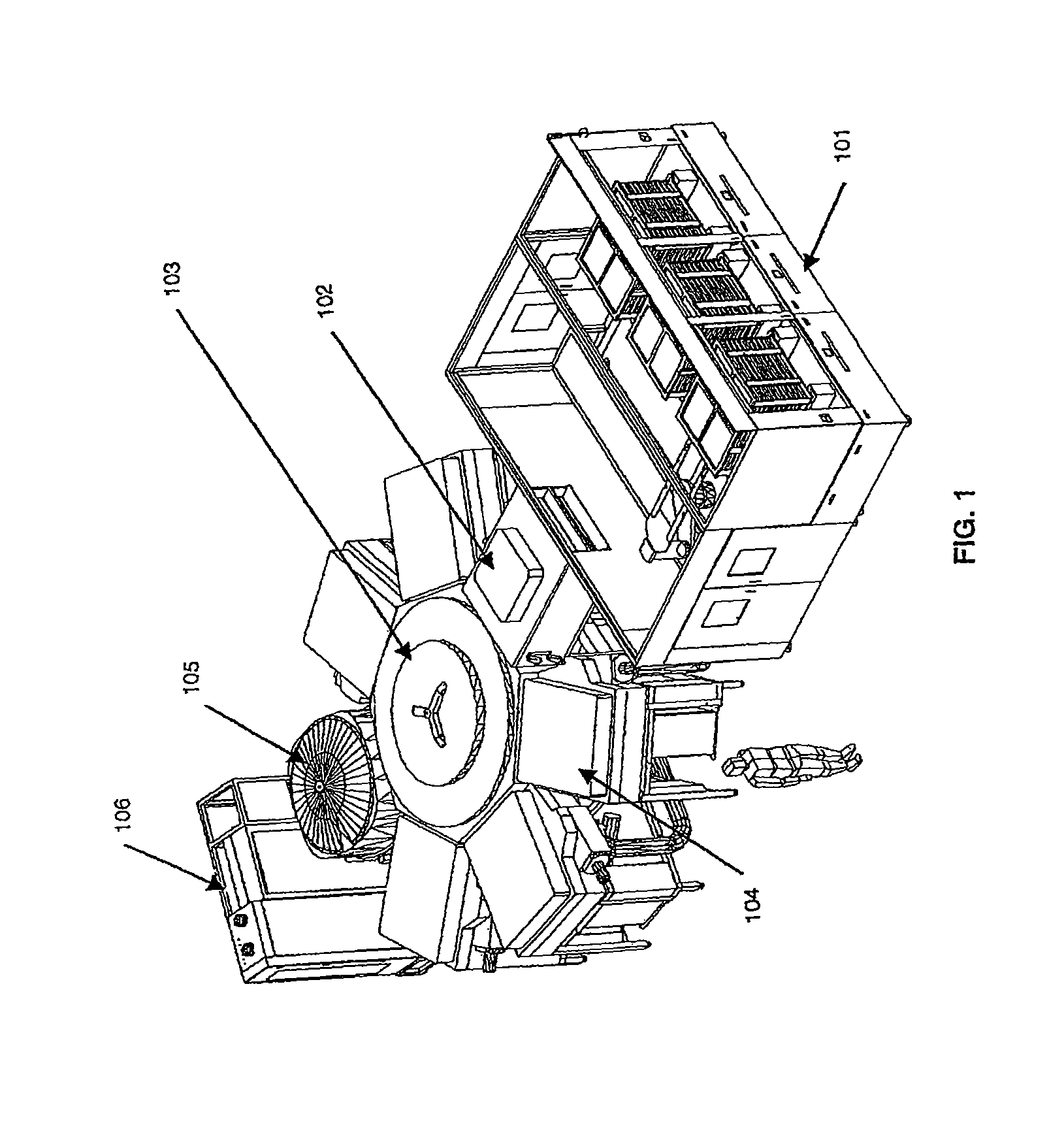
FIG. 1 is an overview of the presently disclosed system, i.e., AKT Gen4 with AGV/MGV interface and atmospheric cassette load station (ACLS), comprising a cassette load station 101, a load lock chamber 102, a central transfer chamber 103, one or more process chambers 104, a heat chamber 105, and control towers and gas chamber 106.
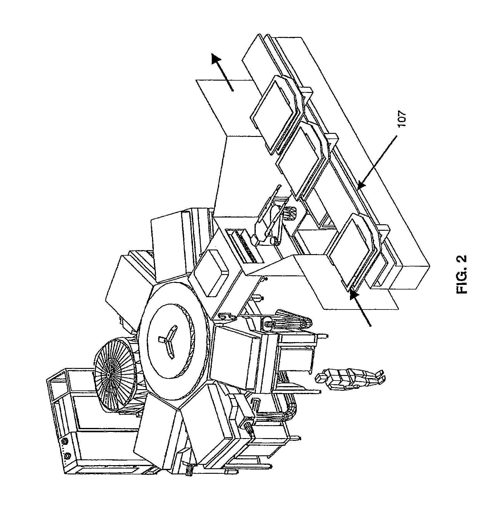
FIG. 2 is an overview of system AKT Gen4 with a substrate transferring link 107.
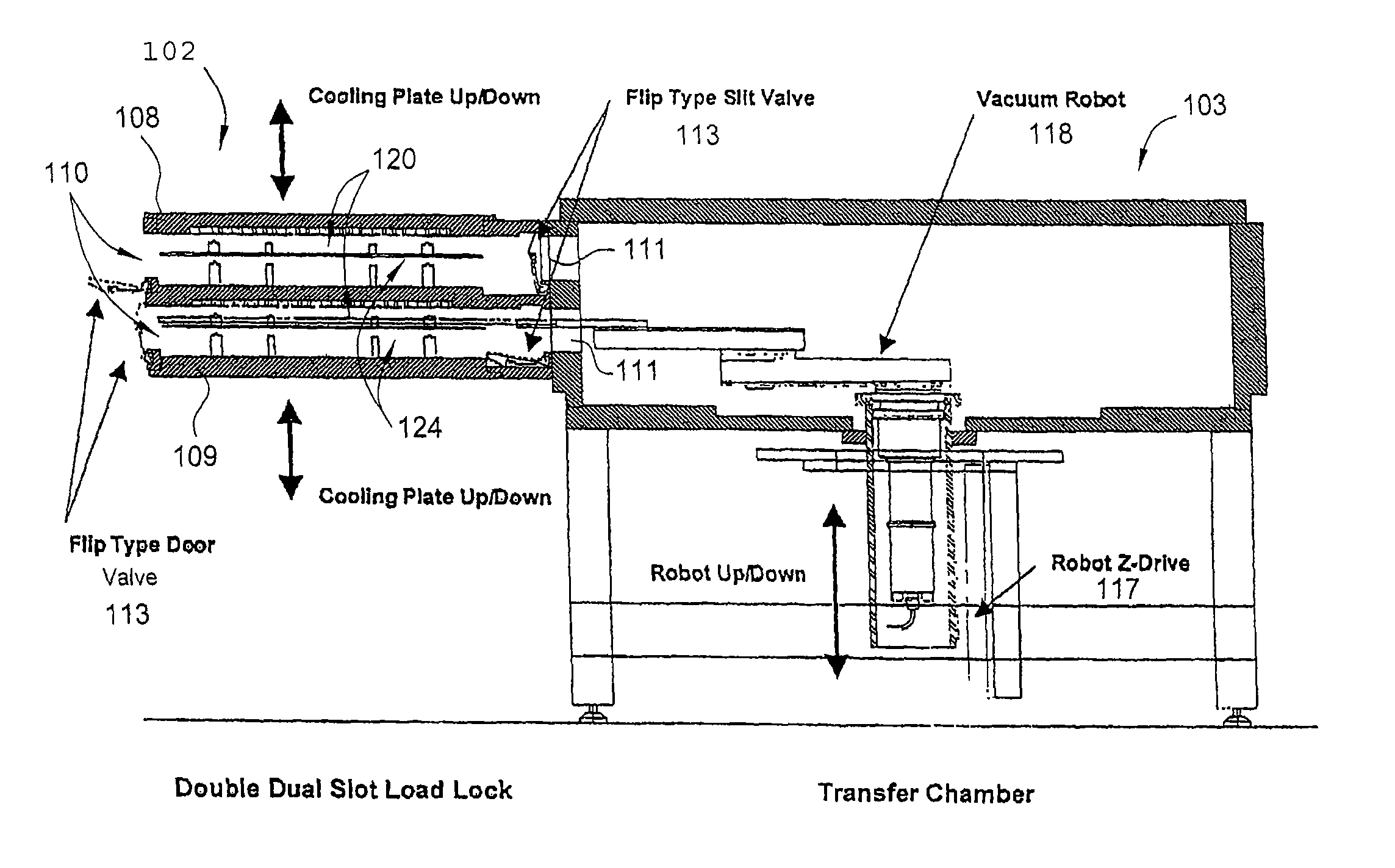
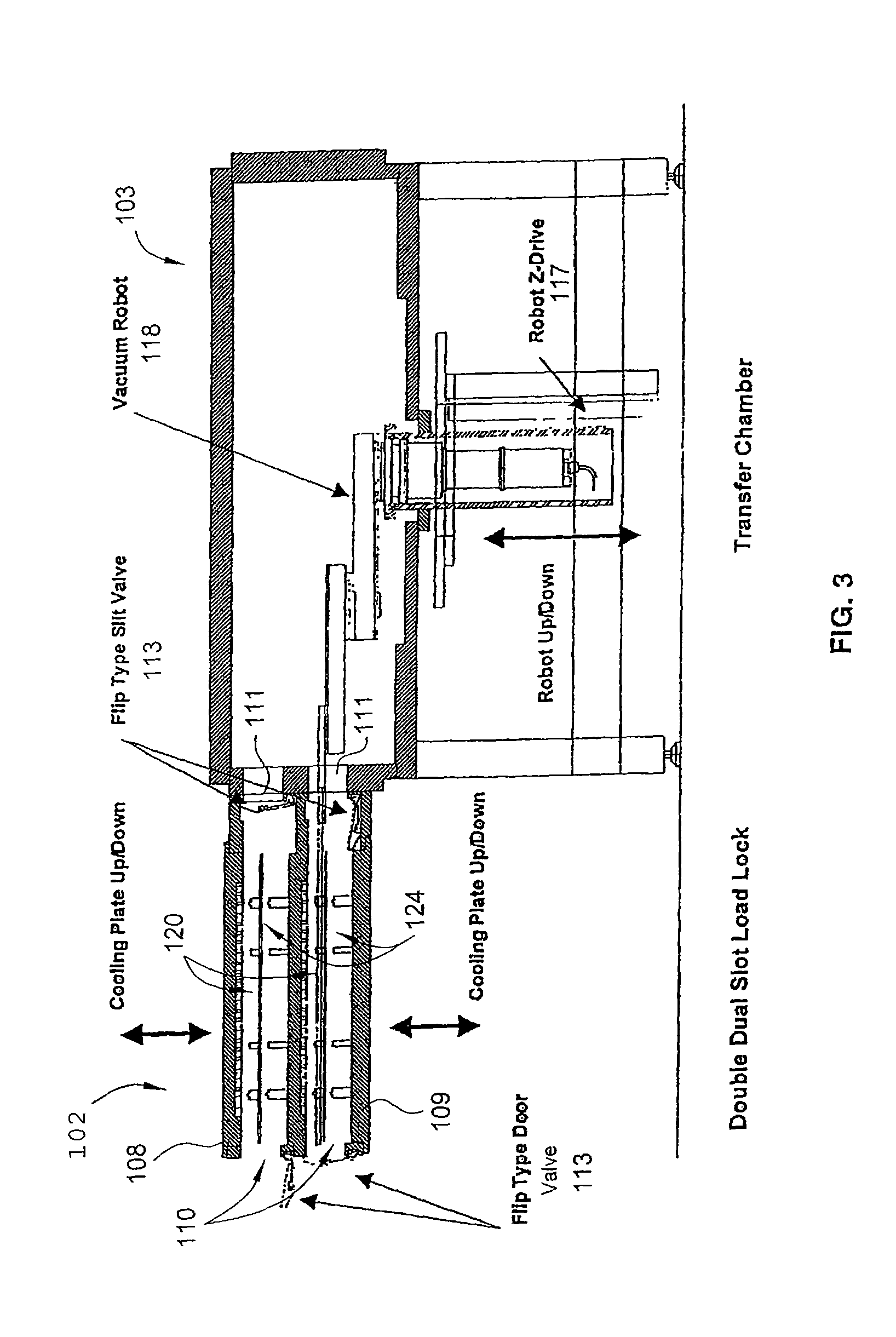
FIG. 3 is a side view of double dual slot load lock and transfer chamber construction in system AKT Gen4.
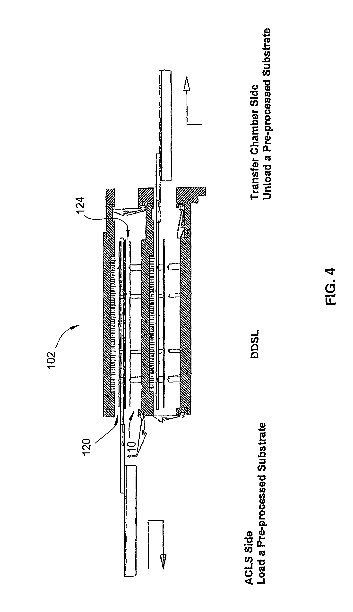
FIG. 4 is a schematic drawing demonstrating loading and unloading of a pre-processed substrate using the double dual slot load lock, wherein the substrate is loaded from ACLS to the upper load lock, and then unloaded to the transfer chamber through the lower load lock.
FIG. 5 is a schematic drawing demonstrating loading and unloading of a pre-processed substrate using the double dual slot load lock, wherein the substrate is loaded from ACLS to the lower load lock, and then unloaded to the transfer chamber through the upper load lock.
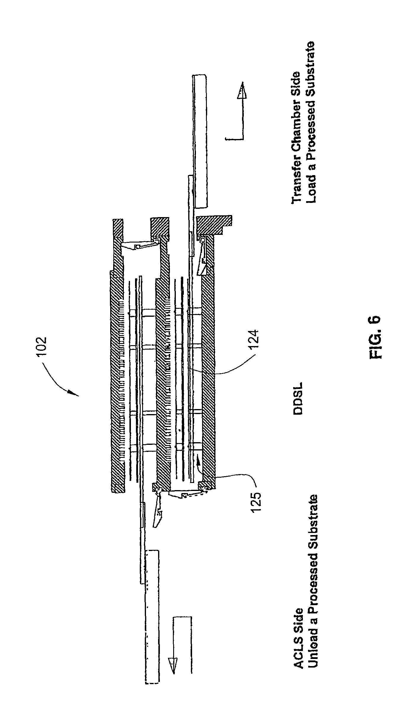
FIG. 6 is a schematic drawing demonstrating loading and unloading of a processed substrate using the double dual slot load lock, wherein the substrate is loaded from the transfer chamber to the lower load lock, and then unloaded to ACLS through the upper load lock.
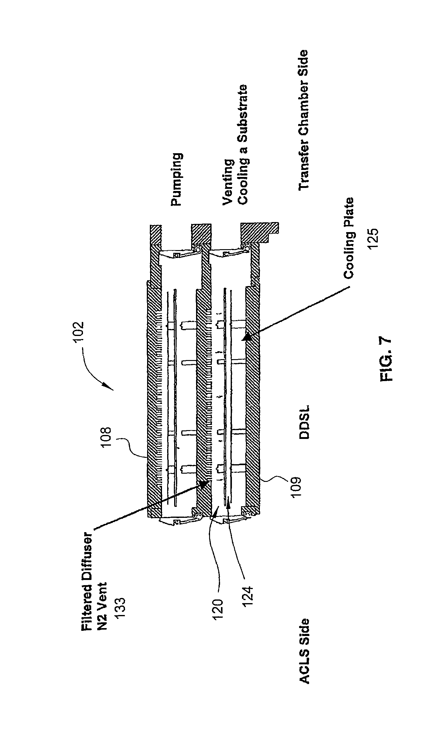
FIG. 7 is a schematic drawing demonstrating pumping and venting processes which take place in the double dual slot load lock. Specifically, filtered diffuser N.sub.2 vent is used for cooling a processed substrate when venting.
FIGS. 8A-8C show system size comparison among AKT5500 150 (state-of-art system) (Figure A), AKT stretch 160 (Figure B), and AKT Gen4 170 (Figure C). The AKT stretch 160 is 133% stretch of AKT5500 150 and a traditional approach to AKT Gen4 170. Both AKT5500 150 and AKT stretch 160 have two dual slot load locks which are constructed at two locations, whereas AKT Gen4 170 has one double dual slot load lock.
DETAILED DESCRIPTION OF THE PREFERRED EMBODIMENT
Provided herein is a semiconductor wafer processing system, comprising a cassette load station 101, load lock chamber 102, a central transfer chamber 103, one or more process chambers 104, a heat chamber 105, and control towers and gas chamber 106 (FIG. 1).
The load lock chamber 102 is provided for transferring wafers between the transfer chamber 103, which is typically at high vacuum, and the outside, typically a clean room at atmospheric pressure. The central transfer chamber 103 is provided with a vacuum transfer robot located therein for transferring wafers between the load lock chamber 102 and the process chambers 104/heat chamber 105, which are located about the periphery of the transfer chamber 103. FIG. 2 is an over view of the system with substrate transferring link 107.
Specifically, the load lock chamber 102 comprises double dual slot load lock constructed at one body (i.e., one location, in one chamber). Each load lock has dual slot load lock (DSL) function: upper slot for loading pre-processed substrate from cassette load station 101 (atmospheric side); and lower slot for unloading processed substrate to cassette load station 101 (atmospheric side). In most cases, the substrate is a wafer or a glass substrate.
Substrates are loaded/unloaded by both vacuum robot and atmospheric robot. Vacuum robot in the central transfer chamber 103 passes substrates through slit valves in the various connected processing chambers 104 or heater chamber 105 and retrieves them after processing in the chambers is complete. Access between the individual process chambers 104 and between the transfer chamber 103 and the load lock chamber 102 is via flip door type slit valves which selectively isolate the process chambers 104 or heat chamber 105 from the robot (in transfer chamber 103) and the robot from the load lock chamber 102. However, the load lock chamber at the atmospheric side may have other than flip door type slit valves. Other doors may also be used to separate the vacuum condition in the load lock chamber from the atmospheric condition outside the chamber.
FIG. 3 is a system side view showing the construction of double dual slot load lock 102 and the transfer chamber 103. The flip type valve 113 is closed from the atmospheric side, which makes it possible to keep load lock vacuum condition with small torque actuator. The valve 113 is always operated below the substrate transferring plane to reduce particle exposure and opens before loading and unloading of a substrate.
This system configuration permits processing in one or more chambers while wafers are being loaded or unloaded at other process chambers or at the load lock chamber 102 and permits wafer transfer from one processing chamber to another via the transfer chamber 103. Different processes may be simultaneously performed on different substrates at different process chambers. Each wafer which is dispensed from load lock may be stepped through the same process steps to produce the same type of wafer. Alternatively, different wafers from the same load lock may be programmed to undergo a different `recipe" involving different steps and/or process times, such that different types of wafers are produced.
Specifically, the vacuum robot 118 was operated by Z-drive 117 in an up-and-down motion. The Z-drive shaft is a vacuum seal constructed in chambers with nitrogen purge and vacuum at the same time.
The above-disclosed system can be used for processing substrates for semiconductor manufacturing. In more specific detail, pre-processed substrates are loaded into the upper slot 120 via opening 110 in one of the load locks from the cassette load station (FIGS. 4-5). The upper slot 120 optionally has a heating plate for heating up the substrates. The heating plate is either a stationary plate or a moving plate. It can approximate to the substrates by Z-drive to increase the heating efficiency. During pumping, the heating temperature can be up to 400.degree. C. The heated substrates are then unloaded from the other load lock via opening 111 to the transfer chamber, and further to the process chambers for processing, or to the heat chamber for either preheating or annealing.
After processing in the chambers is complete, the processed substrates are then unloaded from the lower slot 124 in one of the load locks to the cassette load station (FIG. 6). Lower slot has a cooling plate 125 for cooling down the processed substrates. The cooling plate 125 is either a stationary plate or moving plate and it can approximate to the substrates by Z-drive to increase the cooling efficiency. Also, a small amount of helium gas (He) can be supplied with nitrogen gas (N2) for cooling. Filtered diffuser N2 vent 133 is used to prevent particle generation in the load locks (FIG. 7). During venting, the temperature can be cooled down from 350.degree. C. to 80.degree. C. When operated, each load lock loads and unloads substrates separately. Normally, one is venting and the other is pumping so that the vacuum pump can be shared between the two load locks.
The double dual slot load lock (DDSL) system disclosed herein provides several advantages in comparison with traditional one DSL system, such as AKT5500 or AKT stretch (FIGS. 8A-8C). First, constructing two dual slot load lock at one body (one location) can increase system cost performance, i.e., minimize system footprint and increase system throughput that was restricted by the load lock pumping/venting activity. For a traditional one dual slot load lock system (with 4 process chambers), the system maximum throughput determined by the load lock activity is approximately 30 substrate/hour. In contrast, for one embodiment of the double dual slot load lock system disclosed herein, the system maximum throughput is approximately 60 substrate/hour. For example, a single layer firm (passivation) process has a throughput of approximately 26 substrate/hour for traditional one DSL system, while for one embodiment of the double dual slot load lock system disclosed herein, the passivation process has a throughput of approximately 50 substrate/hour. Since the throughput is restricted by load lock activity, a traditional one DSL system with 3 process chambers has the same throughput as the one with 4 process chambers. For active layer process, a traditional one DSL system (with 4 process chambers) has a throughput of approximately 18 substrate/hour, the same as for one embodiment of the double dual slot load lock system disclosed herein. In this case, the system throughput is the same for both one and double DSL systems, therefore system can use one of the two dual slot load lock. Most customers prefer a system that is capable of switching the process based on the production situation, therefore the system has to be configured to handle quick process. For example, the system can be configured to have shorter process time, or change process time based on process data.
Another advantage of using the presently disclosed double dual slot load lock system is its compact size. The double dual slot load lock system requires narrower atmospheric cassette load station than two DSL systems. For grand transportation, there is an equipment size limitation of approximate 3.0 m in dimension. In one embodiment of the double dual slot load lock system, the transfer chamber is designed in a shape of heptagon and the maximum process chamber quantity is 5. To meet the same size requirement, for two DSL systems, the maximum process chamber quantity would be 3.
Therefore, a substrate processing system is hereby provided, which comprises a cassette load station 101, a load lock chamber 102, a transfer chamber 103, and one or more process chambers 104. The transfer chamber 103 is centrally located, and the multiple process chambers 104 are located about the periphery of the transfer chamber 103. The load lock chamber 102 comprises two dual slot load lock 108, 109 constructed at one location.
Specifically, each dual slot load lock 108, 109 has a heating plate and a cooling plate 125 located in different slots. The heating plate is a stationary plate or moving plate operated by Z-drive, and can heat the temperature up to 400.degree. C. during pumping. Similarly, the cooling plate 125 is a stationary plate or moving plate operated by Z-drive, and can cool the temperature down from about 350.degree. C. to about 80.degree. C. during venting. More specifically, the cooling is achieved by water or by venting using nitrogen gas mixed with helium.
The substrate processing system described herein may further comprise a vacuum robot 118, which is located in the transfer chamber 103 for transferring substrates. The vacuum robot 118 is operated by Z-drive 117. Still, the system may further comprise a flip type door located between the cassette load station 101 and the load lock chamber 102. Flip type slit valves 113 may also be constructed between the load lock chamber 102 and the transfer chamber 103. Such slit valves are closed from atmospheric side and always operated below substrate transferring plane to reduce particle exposure. Still yet, the substrate processing system may further comprise filter diffusers vents 133, which are located in the both dual slot load locks to prevent particle generation.
Further provided is a method of processing substrates using the above-disclosed system for semiconductor manufacturing. This method comprises the steps of moving substrates from the cassette load station to the transfer chamber through the load lock chamber; transferring the substrates from the transfer chamber to the process chambers; processing the substrates in the process chambers; and unloading the processed substrates from the process chambers to the cassette load station through the load lock chamber. In this method, one of the dual slot load locks is in a vacuum condition for unloading preprocessed substrates from the load lock chamber to the transfer chamber, whereas at the same time the other dual slot load lock is in an atmospheric condition for unloading processed substrates from the load lock chamber to the cassette load station.
Furthermore, the pre-processed substrates are heated up to about 400.degree. C. before loading to the transfer chamber. The heated substrates are then transferred to the transfer chamber by a vacuum robot which is driven by Z-drive. After processing, the processed substrates are cooled down from about 350.degree. C. to about 80.degree. C. before loading to the cassette load station. To increase cooling efficiency, a small amount of helium gas is supplied with nitrogen gas. Alternatively, the cooling can be achieved by water.
In this method, one load lock is in a vacuum condition and at the same time, the other load lock is in an atmospheric/venting condition. One vacuum pump is shared between the two load locks. Additionally, filter diffusers are located on both load locks to prevent particle generation. Increased vent speed may also be used to further prevent particle generation.
The system/method disclosed herein provides an improved wafer support and transport means to enable automatic and repetitive moving of individual wafers into and from load locks into, through and between processing chambers while minimizing damage and contamination of wafers. Additionally, using two dual slot load lock constructed in the same chamber increases system cost performance, i.e., minimizes system footprint and increases system throughput that was restricted by the load lock pumping/venting activity.
Any patents or publications mentioned in this specification are indicative of the levels of those skilled in the art to which the invention pertains. These patents and publications are herein incorporated by reference to the same extent as if each individual publication was specifically and individually indicated to be incorporated by reference.
One skilled in the art will readily appreciate that the present invention is well adapted to carry out the objects and obtain the ends and advantages mentioned, as well as those inherent therein. It will be apparent to those skilled in the art that various modifications and variations can be made in practicing the present invention without departing from the spirit or scope of the invention. Changes therein and other uses will occur to those skilled in the art which are encompassed within the spirit of the invention as defined by the scope of the claims.
* * * * *
D00000
D00001
D00002
D00003
D00004
D00005
D00006
D00007
D00008
XML
uspto.report is an independent third-party trademark research tool that is not affiliated, endorsed, or sponsored by the United States Patent and Trademark Office (USPTO) or any other governmental organization. The information provided by uspto.report is based on publicly available data at the time of writing and is intended for informational purposes only.
While we strive to provide accurate and up-to-date information, we do not guarantee the accuracy, completeness, reliability, or suitability of the information displayed on this site. The use of this site is at your own risk. Any reliance you place on such information is therefore strictly at your own risk.
All official trademark data, including owner information, should be verified by visiting the official USPTO website at www.uspto.gov. This site is not intended to replace professional legal advice and should not be used as a substitute for consulting with a legal professional who is knowledgeable about trademark law.