Apparatuses and methods for pure-time, self adopt sampling for row hammer refresh sampling
Wu , et al. May 25, 2
U.S. patent number 11,017,833 [Application Number 16/084,119] was granted by the patent office on 2021-05-25 for apparatuses and methods for pure-time, self adopt sampling for row hammer refresh sampling. This patent grant is currently assigned to Micron Technology, Inc.. The grantee listed for this patent is MICRON TECHNOLOGY, INC.. Invention is credited to Dong Pan, Jun Wu.


| United States Patent | 11,017,833 |
| Wu , et al. | May 25, 2021 |
Apparatuses and methods for pure-time, self adopt sampling for row hammer refresh sampling
Abstract
Apparatuses and methods for pure-time, self-adopt sampling for RHR refresh. An example apparatus includes a memory bank comprising a plurality of rows each associated with a respective row address, and a sampling timing generator circuit configured to provide a timing signal having a plurality of pulses. Each of the plurality of pulses is configured to initiate sampling of a respective row address associated with a row of the plurality of rows to detect a row hammer attack. The sampling timing generator includes first circuitry configured to provide a first subset of pulses of the plurality of pulses during a first time period and includes second circuitry configured to initiate provision of a second subset of pulses of the plurality of pulses during a second time period after the first time period.
| Inventors: | Wu; Jun (Su Zhou, CN), Pan; Dong (Boise, ID) | ||||||||||
|---|---|---|---|---|---|---|---|---|---|---|---|
| Applicant: |
|
||||||||||
| Assignee: | Micron Technology, Inc. (Boise,
ID) |
||||||||||
| Family ID: | 68616301 | ||||||||||
| Appl. No.: | 16/084,119 | ||||||||||
| Filed: | May 24, 2018 | ||||||||||
| PCT Filed: | May 24, 2018 | ||||||||||
| PCT No.: | PCT/CN2018/088203 | ||||||||||
| 371(c)(1),(2),(4) Date: | September 11, 2018 | ||||||||||
| PCT Pub. No.: | WO2019/222960 | ||||||||||
| PCT Pub. Date: | November 28, 2019 |
Prior Publication Data
| Document Identifier | Publication Date | |
|---|---|---|
| US 20200294569 A1 | Sep 17, 2020 | |
| Current U.S. Class: | 1/1 |
| Current CPC Class: | G11C 11/408 (20130101); G11C 11/4078 (20130101); G11C 11/406 (20130101); G11C 11/40618 (20130101) |
| Current International Class: | G11C 7/00 (20060101); G11C 11/406 (20060101) |
References Cited [Referenced By]
U.S. Patent Documents
| 5654929 | August 1997 | Mote, Jr. |
| 5956288 | September 1999 | Bermingham et al. |
| 5959923 | September 1999 | Matteson et al. |
| 5999471 | December 1999 | Choi |
| 6002629 | December 1999 | Kim et al. |
| 6306721 | October 2001 | Teo et al. |
| 6363024 | March 2002 | Fibranz |
| 6392952 | May 2002 | Chen et al. |
| 7002868 | February 2006 | Takahashi |
| 7082070 | July 2006 | Hong |
| 7203113 | April 2007 | Takahashi et al. |
| 8174921 | May 2012 | Kim et al. |
| 8400805 | March 2013 | Yoko |
| 8572423 | October 2013 | Isachar et al. |
| 9236110 | January 2016 | Bains et al. |
| 9251885 | February 2016 | Greenfield et al. |
| 9299400 | March 2016 | Bains et al. |
| 9406358 | August 2016 | Lee |
| 9653139 | May 2017 | Park |
| 9691466 | June 2017 | Kim |
| 9734887 | August 2017 | Tavva |
| 9812185 | November 2017 | Fisch et al. |
| 9818469 | November 2017 | Kim et al. |
| 9865328 | January 2018 | Desimone et al. |
| 10090038 | October 2018 | Shin |
| 10381327 | August 2019 | Ramachandra et al. |
| 10490250 | November 2019 | Ito et al. |
| 10490251 | November 2019 | Wolff |
| 10510396 | December 2019 | Notani et al. |
| 10572377 | February 2020 | Zhang et al. |
| 10573370 | February 2020 | Ito et al. |
| 10685696 | June 2020 | Brown et al. |
| 2002/0026613 | February 2002 | Niiro |
| 2002/0191467 | December 2002 | Matsumoto et al. |
| 2003/0026161 | February 2003 | Yamaguchi et al. |
| 2003/0081483 | May 2003 | De Paor et al. |
| 2003/0161208 | August 2003 | Nakashima et al. |
| 2003/0231540 | December 2003 | Lazar et al. |
| 2004/0024955 | February 2004 | Patel |
| 2005/0002268 | January 2005 | Otsuka et al. |
| 2005/0105362 | May 2005 | Choi et al. |
| 2005/0108460 | May 2005 | David |
| 2005/0213408 | September 2005 | Shieh |
| 2005/0243627 | November 2005 | Lee et al. |
| 2006/0018174 | January 2006 | Park et al. |
| 2006/0104139 | May 2006 | Hur et al. |
| 2006/0215474 | September 2006 | Hokenmaier |
| 2006/0233012 | October 2006 | Sekiguchi et al. |
| 2006/0262617 | November 2006 | Lee |
| 2006/0268643 | November 2006 | Schreck et al. |
| 2007/0002651 | January 2007 | Lee |
| 2007/0028068 | February 2007 | Golding et al. |
| 2007/0147154 | June 2007 | Lee |
| 2007/0263442 | November 2007 | Cornwell et al. |
| 2008/0212386 | September 2008 | Riho |
| 2008/0224742 | September 2008 | Pomichter |
| 2008/0306723 | December 2008 | De Ambroggi et al. |
| 2009/0021999 | January 2009 | Tanimura et al. |
| 2009/0059641 | March 2009 | Jeddeloh |
| 2009/0073760 | March 2009 | Betser et al. |
| 2009/0161468 | June 2009 | Fujioka |
| 2009/0168571 | July 2009 | Pyo et al. |
| 2009/0228739 | September 2009 | Cohen et al. |
| 2009/0296510 | December 2009 | Lee et al. |
| 2010/0005217 | January 2010 | Jeddeloh |
| 2010/0097870 | April 2010 | Kim et al. |
| 2010/0141309 | June 2010 | Lee |
| 2010/0182863 | July 2010 | Fukiage |
| 2011/0225355 | September 2011 | Kajigaya |
| 2011/0299352 | December 2011 | Fujishiro |
| 2012/0014199 | January 2012 | Narui |
| 2012/0155173 | June 2012 | Lee et al. |
| 2012/0155206 | June 2012 | Kodama |
| 2012/0287727 | November 2012 | Wang |
| 2012/0307582 | December 2012 | Marumoto et al. |
| 2012/0327734 | December 2012 | Sato |
| 2013/0028034 | January 2013 | Fujisawa |
| 2013/0051157 | February 2013 | Park |
| 2013/0051171 | February 2013 | Porter et al. |
| 2014/0006700 | January 2014 | Schaefer et al. |
| 2014/0006703 | January 2014 | Bains et al. |
| 2014/0016422 | January 2014 | Kim et al. |
| 2014/0022858 | January 2014 | Chen et al. |
| 2014/0043888 | February 2014 | Chen et al. |
| 2014/0089758 | March 2014 | Kwok et al. |
| 2014/0095780 | April 2014 | Bains et al. |
| 2014/0119091 | May 2014 | You et al. |
| 2014/0143473 | May 2014 | Kim et al. |
| 2014/0177370 | June 2014 | Halbert et al. |
| 2014/0181453 | June 2014 | Jayasena et al. |
| 2014/0185403 | July 2014 | Lai |
| 2014/0189228 | July 2014 | Greenfield et al. |
| 2014/0321226 | October 2014 | Pyeon |
| 2015/0016203 | January 2015 | Sriramagiri et al. |
| 2015/0049566 | February 2015 | Lee et al. |
| 2015/0049567 | February 2015 | Chi |
| 2015/0078112 | March 2015 | Huang |
| 2015/0092508 | April 2015 | Bains |
| 2015/0109871 | April 2015 | Bains et al. |
| 2015/0213872 | July 2015 | Mazumder et al. |
| 2015/0294711 | October 2015 | Gaither et al. |
| 2015/0356048 | December 2015 | King |
| 2015/0380073 | December 2015 | Joo |
| 2016/0070483 | March 2016 | Yoon et al. |
| 2016/0086649 | March 2016 | Ho |
| 2016/0155491 | June 2016 | Roberts et al. |
| 2016/0180917 | June 2016 | Chishti et al. |
| 2016/0180921 | June 2016 | Jeong |
| 2016/0202926 | July 2016 | Benedict |
| 2016/0225433 | August 2016 | Bains et al. |
| 2016/0343423 | November 2016 | Shido |
| 2017/0011792 | January 2017 | Oh et al. |
| 2017/0052722 | February 2017 | Ware et al. |
| 2017/0092350 | March 2017 | Halbert et al. |
| 2017/0111792 | April 2017 | Correia Fernandes et al. |
| 2017/0133085 | May 2017 | Kim et al. |
| 2017/0140807 | May 2017 | Sun et al. |
| 2017/0140810 | May 2017 | Choi et al. |
| 2017/0140811 | May 2017 | Joo |
| 2017/0146598 | May 2017 | Kim et al. |
| 2017/0148504 | May 2017 | Saifuddin et al. |
| 2017/0186481 | June 2017 | Oh et al. |
| 2017/0269861 | September 2017 | Lu et al. |
| 2017/0287547 | October 2017 | Ito et al. |
| 2017/0345482 | November 2017 | Balakrishnan |
| 2017/0352404 | December 2017 | Lee et al. |
| 2018/0005690 | January 2018 | Morgan et al. |
| 2018/0025770 | January 2018 | Ito et al. |
| 2018/0025772 | January 2018 | Lee et al. |
| 2018/0025773 | January 2018 | Bains et al. |
| 2018/0047110 | February 2018 | Blackman et al. |
| 2018/0061476 | March 2018 | Kim |
| 2018/0061483 | March 2018 | Morgan |
| 2018/0075927 | March 2018 | Jeong et al. |
| 2018/0096719 | April 2018 | Tomishima et al. |
| 2018/0108401 | April 2018 | Choi et al. |
| 2018/0114561 | April 2018 | Fisch et al. |
| 2018/0114565 | April 2018 | Lee |
| 2018/0122454 | May 2018 | Lee et al. |
| 2018/0130506 | May 2018 | Kang et al. |
| 2018/0137005 | May 2018 | Wu et al. |
| 2018/0158504 | June 2018 | Akamatsu |
| 2018/0158507 | June 2018 | Bang |
| 2018/0190340 | July 2018 | Kim et al. |
| 2018/0218767 | August 2018 | Wolff |
| 2018/0226119 | August 2018 | Kim et al. |
| 2018/0233197 | August 2018 | Laurent |
| 2018/0240511 | August 2018 | Yoshida et al. |
| 2018/0247876 | August 2018 | Kim et al. |
| 2018/0254078 | September 2018 | We et al. |
| 2018/0261268 | September 2018 | Hyun et al. |
| 2018/0294028 | October 2018 | Lee et al. |
| 2018/0308539 | October 2018 | Ito et al. |
| 2018/0341553 | November 2018 | Koudele et al. |
| 2019/0065087 | February 2019 | Li et al. |
| 2019/0066759 | February 2019 | Nale |
| 2019/0066766 | February 2019 | Lee |
| 2019/0088315 | March 2019 | Saenz et al. |
| 2019/0088316 | March 2019 | Inuzuka et al. |
| 2019/0122723 | April 2019 | Ito |
| 2019/0129651 | May 2019 | Wuu et al. |
| 2019/0161341 | May 2019 | Howe |
| 2019/0190341 | June 2019 | Beisele et al. |
| 2019/0196730 | June 2019 | Imran |
| 2019/0205253 | July 2019 | Roberts |
| 2019/0252020 | August 2019 | Rios et al. |
| 2019/0279706 | September 2019 | Kim |
| 2019/0294348 | September 2019 | Ware et al. |
| 2019/0333573 | October 2019 | Shin et al. |
| 2019/0362774 | November 2019 | Kuramori et al. |
| 2019/0385661 | December 2019 | Koo et al. |
| 2019/0385667 | December 2019 | Morohashi et al. |
| 2019/0385668 | December 2019 | Fujioka et al. |
| 2019/0385670 | December 2019 | Notani et al. |
| 2019/0391760 | December 2019 | Miura et al. |
| 2019/0392886 | December 2019 | Cox et al. |
| 2020/0005857 | January 2020 | Ito et al. |
| 2020/0051616 | February 2020 | Cho |
| 2020/0075086 | March 2020 | Hou et al. |
| 2020/0082873 | March 2020 | Wolff |
| 2020/0126611 | April 2020 | Riho et al. |
| 2020/0135263 | April 2020 | Brown et al. |
| 2020/0143871 | May 2020 | Kim et al. |
| 2020/0176050 | June 2020 | Ito et al. |
| 2020/0194056 | June 2020 | Sakurai et al. |
| 2020/0210278 | July 2020 | Rooney et al. |
| 2020/0211633 | July 2020 | Okuma |
| 2020/0211634 | July 2020 | Ishikawa et al. |
| 2020/0219556 | July 2020 | Ishikawa et al. |
| 2020/0265888 | August 2020 | Ito et al. |
| 2020/0273517 | August 2020 | Yamamoto |
| 2020/0273518 | August 2020 | Raad et al. |
| 2020/0279599 | September 2020 | Ware et al. |
| 2020/0321049 | October 2020 | Meier et al. |
| 104350546 | Feb 2015 | CN | |||
| 106710621 | May 2017 | CN | |||
| 107871516 | Apr 2018 | CN | |||
| 4911510 | Jan 2012 | JP | |||
| 6281030 | Jan 2018 | JP | |||
| 2019222960 | Nov 2019 | WO | |||
| 2020010010 | Jan 2020 | WO | |||
| 2020117686 | Jun 2020 | WO | |||
Other References
|
International Search Report and Written Opinion for Application No. PCT/US2019/040169, dated Oct. 25, 2019. cited by applicant . U.S. Appl. No. 16/537,981 titled "Apparatuses and Methods for Controlling Targeted Refresh Rates" filed Aug. 12, 2019. cited by applicant . U.S. Appl. No. 16/655,110 titled "Apparatuses and Methods for Dynamic Targeted Refresh Steals" filed Oct. 16, 2019. cited by applicant . U.S. Appl. No. 16/549,411 titled "Apparatuses and Methods for Dynamic Refresh Allocation" filed Aug. 23, 2019. cited by applicant . U.S. Appl. No. 16/682,606, titled "Apparatuses and Methods for Distributing Row Hammer Refresh Events Across a Memory Device", filed Nov. 13, 2019. cited by applicant . International Search Report & Written Opinion dated Mar. 24, 2020 for PCT Application No. PCT/US2019/064028, 11 pages. cited by applicant . U.S. Appl. No. 16/818,989, titled "Semiconductor Device Performing Row Hammer Refresh Operation", dated Mar. 13, 2020. cited by applicant . U.S. Appl. No. 16/818,981 titled "Apparatuses and Methods for Staggered Timing of Targeted Refresh Operations" filed Mar. 13, 2020. cited by applicant . U.S. Appl. No. 16/824,460, titled "Semiconductor Device Performing Row Hammer Refresh Operation", dated Mar. 19, 2020. cited by applicant . U.S. Appl. No. 16/886,284, titled "Apparatuses and Methods for Access Based Refresh Timing", dated May 28, 2020. cited by applicant . International Search Report and Written Opinion dated Feb. 20, 2019 for PCT Application No. PCT/CN2018/088203, 9 pages. cited by applicant . U.S. Appl. No. 16/025,844, titled "Apparatus and Methods for Triggering Row Hammer Address Sampling", filed Jul. 2, 2018. cited by applicant . U.S. Appl. No. 16/176,932, titled "Apparatuses and Methods for Access Based Refresh Timing", filed Oct. 31, 2018. cited by applicant . U.S. Appl. No. 16/230,300, titled "Apparatuses and Methods for Staggered Timing of Targeted Refresh Operations" filed Dec. 21, 2018. cited by applicant . U.S. Appl. No. 16/232,837, titled "Apparatuses and Methods for Distributed Targeted Refresh Operations", filed Dec. 26, 2018. cited by applicant . U.S. Appl. No. 16/286,187 titled "Apparatuses and Methods for Memory Mat Refresh Sequencing" filed Feb. 26, 2019. cited by applicant . U.S. Appl. No. 16/290,730, titled "Semiconductor Device Performing Row Hammer Refresh Operation", filed Mar. 1, 2019. cited by applicant . U.S. Appl. No. 16/374,623, titled "Semiconductor Device Performing Row Hammer Refresh Operation", filed Apr. 3, 2019. cited by applicant . U.S. Appl. No. 16/375,716 titled "Stagger RHR Pumping Scheme Across Die Banks" filed Apr. 4, 2019; pp. all. cited by applicant . U.S. Appl. No. 16/431,641 titled "Apparatuses and Methods for Controlling Steal Rates" filed Jun. 4, 2019. cited by applicant . International Search Report & Written Opinion dated Aug. 28, 2020 for PCT Application No. PCT/US2020/032931. cited by applicant . International Search Report and Written Opinion for PCT/US2020/026689 dated Jul. 22, 2020. cited by applicant . U.S. Appl. No. 17/008,396 titled "Apparatuses and Methods for Staggered Timing of Targeted Refresh Operations" filed Aug. 31, 2020. cited by applicant . U.S. Appl. No. 16/997,766 titled "Refresh Logic Circuit Layouts Thereof" filed Aug. 19, 2020. cited by applicant . U.S. Appl. No. 17/095,978 titled "Apparatuses and Methods for Controlling Refresh Timing" filed Nov. 12, 2020. cited by applicant . U.S. Appl. No. 17/030,018, titled "Apparatuses and Methods for Controlling Refresh Operations", filed Sep. 23, 2020. cited by applicant . U.S. Appl. No. 17/175,485 titled "Apparatuses and Methods for Distributed Targeted Refresh Operations" filed Feb. 12, 2021. cited by applicant . U.S. Appl. No. 17/186,913 titled "Apparatuses and Methods for Dynamic Refresh Allocation" filed Feb. 26, 2021. cited by applicant . U.S. Appl. No. 17/187,002 titled "Apparatuses and Methods for Staggered Timing of Targeted Refresh Operations" filed Feb. 26, 2021. cited by applicant. |
Primary Examiner: Nguyen; Hien N
Attorney, Agent or Firm: Dorsey & Whitney LLP
Claims
What is claimed is:
1. An apparatus comprising: a memory bank comprising a plurality of rows each associated with a respective row address; and a sampling timing generator circuit configured to provide a timing signal having a plurality of pulses, wherein each of the plurality of pulses is configured to initiate sampling of a respective row address associated with a row of the plurality of rows to detect a row hammer attack, wherein the sampling timing generator includes first circuitry configured to provide a first subset of pulses of the plurality of pulses during a first time period and includes second circuitry configured to initiate provision of a second subset of pulses of the plurality of pulses during a second time period after the first time period.
2. The apparatus of claim 1, wherein the length of the first time period equal to the length of the second time period.
3. The apparatus of claim 1, wherein a length of the first time period is set based on a maximum value of a first counter and an oscillation signal, and wherein a length of the second time period is set based on a maximum value of a second counter and the oscillation signal.
4. The apparatus of claim 3, wherein first circuitry is configured to provide the first subset of pulses while a latched count value is different than a count value of a third counter, wherein the third counter is incremented in response to each of the first subset of pulses.
5. The apparatus of claim 4, wherein the second circuitry is configured to initiate provision of the second subset of pulses by the first circuit during the second time period based on a random count value.
6. The apparatus of claim 5, wherein the second circuitry is configured to initiate provision of the second subset of pulses by the first circuitry during the second time period when the random count value has a first value.
7. The apparatus of claim 6, wherein the second circuitry is configured to skip provision of the second subset of pulses by the first circuitry during the second time period when the random count value has a second value.
8. The apparatus of claim 6, wherein the second circuitry is configured to initiate provision of a third subset of pulses of the plurality of pulses by the first circuitry during a third time period when the random count value has a second value.
9. The apparatus of claim 3, wherein the sampling timing generator circuit comprises a logic circuit configured to transmit the oscillation signal.
10. The apparatus of claim 1, wherein the second circuitry is configured to be reset to the first time period in response to a row hammer refresh signal being set.
11. An apparatus comprising: a plurality of memory banks, wherein each memory bank of the plurality of memory banks, includes a latch configured to store an address for interrupt refresh; and a sampling timing generator circuit configured to receive an oscillation signal, wherein the sampling timing generator circuit comprises first circuitry configured to provide a first set of pulses on a trigger signal to sample the address during a first time period, wherein the sampling timing generator circuit further comprises second circuitry configured to determine whether to initiate provision of a second set of pulses on the trigger signal to sample the address during a second time period, wherein the first time period and the second time period are non-overlapping time periods.
12. The apparatus of claim 11, wherein the second circuitry is configured to initiate the second set of pulses during the second time period in response to a random counter providing a first value, wherein the second circuitry is configured to skip initiation of the second set of pulses during the second time period in response to the random counter circuit providing a second value.
13. The apparatus of claim 11, the second circuitry is configured to be reset to the first time period, in response to a row hammer refresh signal being set.
14. The apparatus of claim 11, wherein the first circuitry includes a counter and a latch, wherein during the first time period the latch is configured to latch a first random value of the counter during the first time period, wherein, in response to the second circuitry determining to initiate the second set of pulses, the latch is configured to latch a second random value of the counter during the second time period.
15. The apparatus of claim 14, wherein a count of the first set of pulses is equal to the first random value and wherein a count of the second set of pulses is equal to the second random value.
16. The apparatus of claim 11, wherein the first time period and the second time period both occur within a same row hammer refresh interval.
17. A method comprising: during a first time period of a row hammer refresh interval, providing a first subset of pulses on a timing signal from a sampling timing generator circuit to trigger sampling of a respective row address associated with a row of a plurality of rows of a memory bank; and during a second time period of the row hammer refresh interval after the first time period, initiating provision of a second subset of pulses on the timing signal.
18. The method of claim 17, wherein initiating provision of the second subset of pulses is in response to a random counter circuit providing a first count value.
19. The method of claim 17, wherein the length of the first time period equal to the length of the second time period.
20. The method of claim 17, further comprising resetting to the first time period at a start of a second row hammer refresh interval.
Description
RELATED APPLICATIONS
This application is a 371 National Stage application claiming priority to PCT Application No. PCT/CN2018/088203, filed May 24, 2018, which application is incorporated herein by reference in its entirety, for any purpose.
BACKGROUND
High data reliability, high speed of memory access, and reduced chip size are features that are demanded from semiconductor memory. A dynamic random access memory (DRAM), which is a typical semiconductor memory device, stores information by charges accumulated in cell capacitors, and, therefore, the information is lost unless refresh operations are periodically carried out. The information may be further lost as bit errors due to Row Hammer effects and/or Ras-Clobber effects. In either case, such bit errors may take place on one or more memory cells each coupled to a non-selected word line that is adjacent to a selected word line subjected to Row Hammer (indicating that the selected word line is driven to an active level a great number of times successively) or Ras-Clobber (indicating that the selected word line is driven to the active level continuously for a considerably long period). The memory cells coupled to such non-selected word line are thus required to be refreshed prior to losing the information stored therein. On the other hand, auto-refresh (AREF) commands indicating refresh operations are periodically issued from a control device such as a memory controller, which controls a DRAM. The AREF commands are provided from the control device at a frequency that all the word lines are certainly refreshed once in the one refresh cycle (for example, 64 msec). However, refresh addresses according to the AREF commands are determined by a refresh counter provided in DRAM. For this reason, refresh operations responsive to the AREF commands may not prevent bit errors due to Row Hammer effects and/or Ras-Clobber effects. Thus, steal-refresh is carried out to perform Row Hammer refresh (RHR) operations in which some of refresh operations responsive to the AREF commands are stolen therefrom and then allocated to the RHR operations to refresh the memory cells coupled to the non-selected word line that is adjacent to the selected word line subjected to Row Hammer and/or Ras-Clobber.
One way to dynamically control the steal-refresh is time-based random sampling of a row address by randomizing timings for sampling. However, some implementations that use random sampling can have periods where no sampling is taking place if the time between RHR operations is too long.
SUMMARY
Example apparatuses are described herein. An example apparatus may include a memory bank comprising a plurality of rows each associated with a respective row address, and a sampling timing generator circuit configured to provide a timing signal having a plurality of pulses. Each of the plurality of pulses is configured to initiate sampling of a respective row address associated with a row of the plurality of rows to detect a row hammer attack. The sampling timing generator includes first circuitry configured to provide a first subset of pulses of the plurality of pulses during a first time period and includes second circuitry configured to initiate provision of a second subset of pulses of the plurality of pulses during a second time period after the first time period.
Another example method may include a plurality of memory banks. Each memory bank of the plurality of memory banks includes a latch configured to store an address for interrupt refresh. The example apparatus may further include a sampling timing generator circuit configured to receive an oscillation signal. The sampling timing generator circuit comprises first circuitry configured to provide a first set of pulses on a trigger signal to sample the address during a first time period. The sampling timing generator circuit further comprises second circuitry configured to determine whether to initiate provision of a second set of pulses on the trigger signal to sample the address during a second time period. The first time period and the second time period are non-overlapping time periods.
Example methods are described herein. An example method may include, during a first time period of a row hammer refresh interval, providing a first subset of pulses on a timing signal from a sampling timing generator circuit to trigger sampling of a respective row address associated with a row of a plurality of rows of a memory bank, and during a second time period of the row hammer refresh interval after the first time period, initiating provision of a second subset of pulses on the timing signal.
BRIEF DESCRIPTION OF THE DRAWINGS
FIG. 1A depicts a block diagram of a semiconductor device in accordance with an embodiment of the disclosure.
FIG. 2A depicts a circuit diagram a sampling circuit in accordance with an embodiment of the disclosure.
FIG. 2B depicts a timing diagram of signals in the sampling circuit of FIG. 2A in accordance with an embodiment of the present disclosure.
FIGS. 3A and 3B depicts a schematic diagram of a sampling timing generator circuit and a RHR self-refresh oscillator circuit in accordance with an embodiment of the disclosure.
FIG. 4 depicts an exemplary timing diagram associated with operation of a sampling timing generator circuit in accordance with an embodiment of the disclosure.
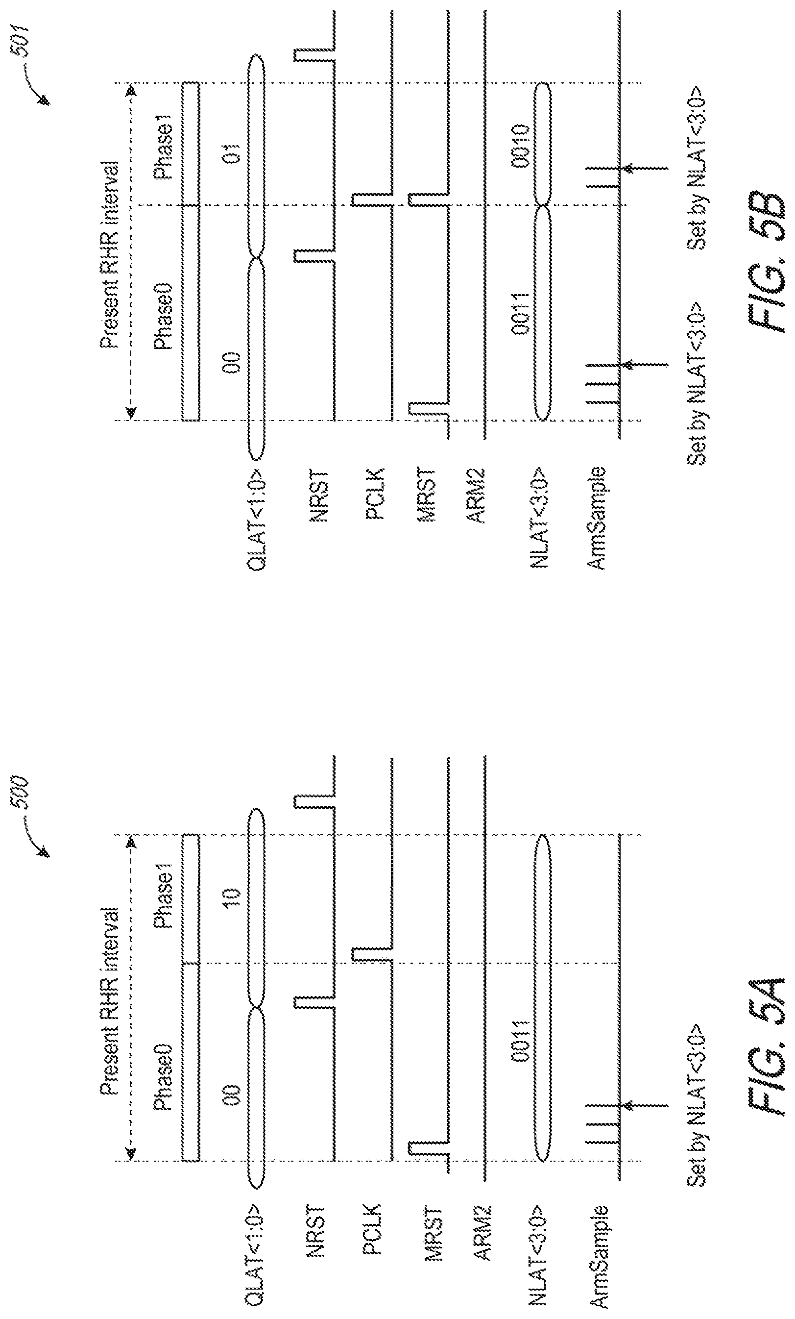
FIGS. 5A and 5B depict exemplary timing diagrams associated with operation of a sampling timing generator circuit in accordance with some embodiments of the disclosure.
DETAILED DESCRIPTION OF PREFERRED EMBODIMENTS
Various embodiments of the present disclosure will be explained below in detail with reference to the accompanying drawings. The following detailed description refers to the accompanying drawings that show, by way of illustration, specific aspects and embodiments of the disclosure. These embodiments are described in sufficient detail to enable those skilled in the art to practice various embodiments of the disclosure. Other embodiments may be utilized, and structure, logical and electrical changes may be made without departing from the scope of the disclosure. The various embodiments disclosed herein are not necessary mutually exclusive, as some disclosed embodiments can be combined with one or more other disclosed embodiments to form new embodiments.
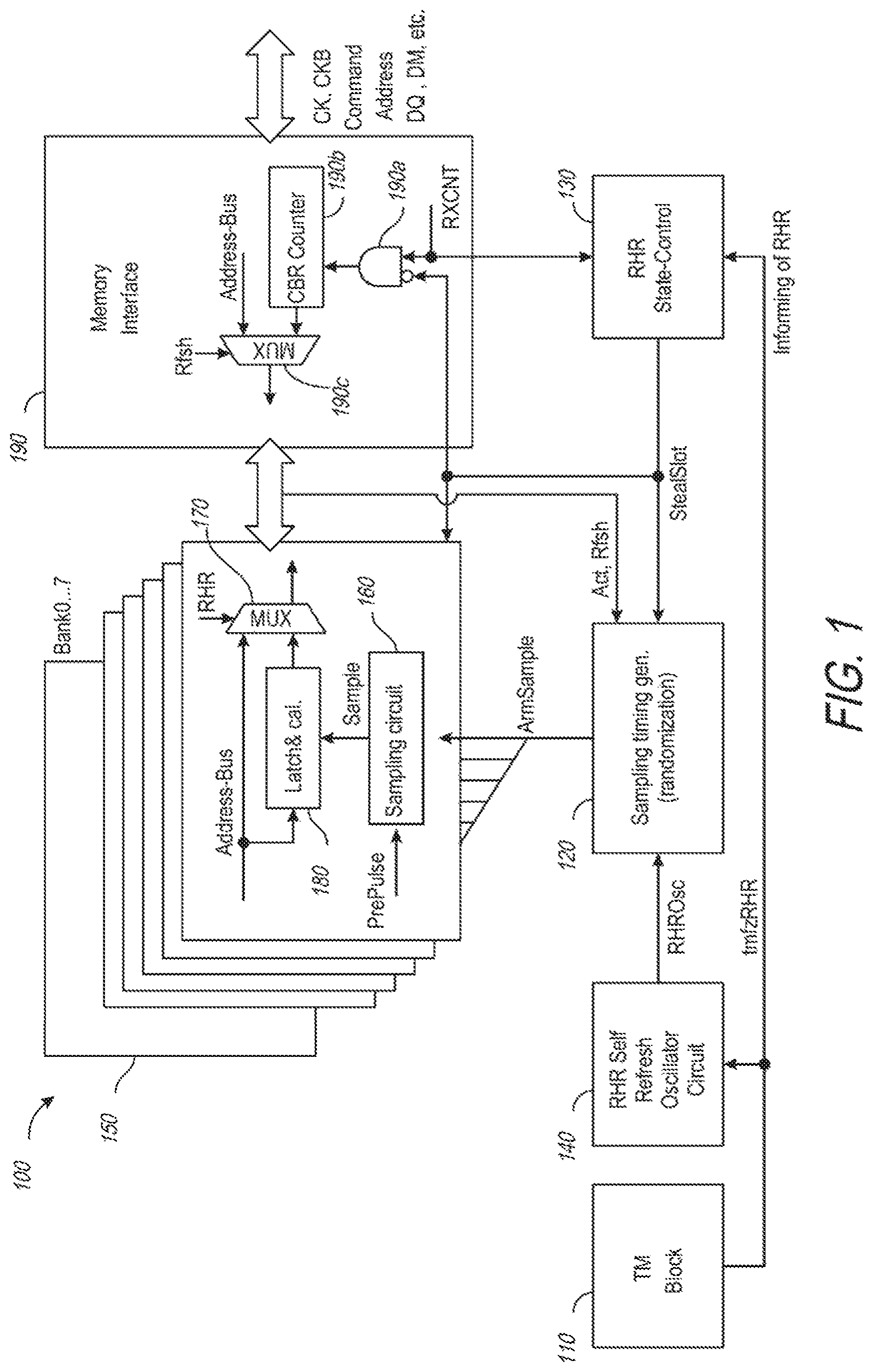
FIG. 1 is a block diagram of a semiconductor device 100 in accordance with embodiments of the disclosure. The semiconductor device 100 may include a plurality of memory banks 150 and a sampling, timing generator circuit 120, and a plurality of sampling circuits 160 associated with the plurality of corresponding memory banks 150, in accordance with an embodiment of the disclosure. The semiconductor device 100 may be a semiconductor memory integrated into a single semiconductor chip, for example, an LPDDR4 SDRAM. The semiconductor device 100 may further include a memory interface circuit 190 (e.g., DRAM interface), a row hammer refresh (RHR) state control circuit 130, the sampling timing generator circuit 120, a RHR self-refresh oscillator circuit 140 and a test mode (TM) block 110. For example, the memory interface circuit 190 may be a DRAM interface that may receive and transmit clock signals, command signals, address signals and data signals, etc.
The TM block 110 may provide a steal rate control signal tmfzRHR in order to adjust a steal rate. The steal rate is a rate at which RHR enters into a test mode. The RHR self-refresh oscillator circuit 140 may control a frequency (cycle) of a frequency-divided RHR oscillation signal (RHROsc), responsive, at least in part, to the steal rate control signal tmfzRHR. The RHROsc signal may be used as a clock signal for signaling an internal cycle. The row hammer refresh (RHR) state control circuit 130 may provide an instruction signal StealSlot that is an instruction signal for executing steal-refresh (or RHR) operations instead of normal refresh based on each auto-refresh (AREF) command. For example, the RHR state-control circuit 130 may receive the steal rate control signal tmfzRHR and an RXCNT signal and may provide an instruction signal StealSlot for executing steal-refresh (or RHR) instead of normal refresh. The RXCNT signal is a clock signal obtained from an auto-refresh (AREF) command, and the RXCNT signal is provided to a refresh counter (CBR counter) 190b in the memory interface circuit 190 and the RHR state-control circuit 130.
The sampling timing generator circuit 120 may be provided in common for the plurality of memory banks 150 in FIG. 1. The sampling timing generator circuit 120 may receive the instruction signal StealSlot from the RHR state-control circuit 130 and may further receive the frequency-divided RHR oscillation signal (RHROsc) from the RHR self-refresh oscillator circuit 140 for self-refresh. The sampling timing generator circuit 120 may provide a trigger signal for sampling (ArmSample) to each sampling circuit 160 of each memory bank of the plurality of memory banks 15 (e.g., Bank 0, . . . Bank 7) at a random timing. The ArmSample signal may be randomized by randomization of a frequency of the activation of the ArmSample signal and randomization of a difference between an interval of RHR execution (e.g., each time auto-refresh command is provided) and an interval (e.g., a cycle) of the frequency-divided RHR oscillation signal (RhrOsc). Because a RHR interval length can be random, with some timing intervals significantly larger than others, some conventional circuitry may have periods where no sampling is taking place during the RHR interval, which may pose a risk to a row hammer attack during these extended RHR intervals. To mitigate effects of these no sampling time periods, the sampling timing generator circuit 120 may include circuitry that is configured to initiate trigger of randomized sampling during longer RHR intervals. The circuitry delineates timing periods, from an initial time period PHASE0 to a last time period PHASE4. Each of the timing phases PHASE0-PHASE3 may have a duration of based on a preset maximum counter value. The last time period PHASE4 may persist until an end of the RHR interval. It is appreciated that greater or fewer time periods could be included without departing from the scope of the disclosure. The circuitry may utilize a random count value to randomly initiate a sampling event during the PHASE1 to PHASE4 time periods. This randomized sampling may provide sampling coverage during extended RHR intervals, which is improved over current time-based solutions that have sampling gaps.
The sampling circuit 160 may provide a sampling signal (Sample) responsive to the ArmSample signal and further to a next PrePulse signal that is generated upon a receipt of a precharge command. A latch and calculator 180 (e.g., a latch, a flip-flop, etc.) of each memory bank of the plurality of memory banks 150 (e.g., Bank0, . . . Bank7) may capture (e.g., latch) a row (X) address on an address bus responsive to the sampling signal (Sample). The row address on the address bus is to access a memory array (not shown) provided in each memory bank of the plurality of memory banks 150 (e.g., Bank0, . . . Bank7). The latch and calculator 180 further may calculate an adjacent address of the latched row address and may provide the adjacent address as an RHR refresh address.
A multiplexer MUX 170 may be a switch that may work as a refresh circuit configured to perform a steal-refresh operation to refresh a memory cell designated by the RHR refresh address. The multiplexer MUX 170 may receive the adjacent address from the latch and calculator 180 and the row address from the address bus, and provide either one of the adjacent address and the row address, responsive to an RHR signal that is generated from Rfsh signal. The Rfsh signal may be generated while receiving the auto-refresh (AREF) command. In the RHR operation, the multiplexer MUX 170 may provide the adjacent address responsive to the RHR signal in an active state. The multiplexer MUX 170 may provide the row address responsive to the RHR signal in an inactive state. Thus, either the row address or the adjacent address most recently captured becomes a valid address that is provided to the memory array in the corresponding memory bank.
The row address to the multiplexer MUX 170 may be provided by a multiplexer MUX 190c of the interface circuit 190. The multiplexer MUX 190c may receive an access row address associated with an active command for data reading or writing supplied to the memory interface 190 through an address bus. The multiplexer MUX 190c may further receive a refresh address from a refresh counter (CBR counter) 190b. The CBR counter 190b may receive a logic AND signal of the RXCNT signal and an inverted signal of the instruction signal for RHR execution StealSlot via a logic AND circuit 190a. The refresh counter (CBR counter) 190b may be stopped when the RHR state-control circuit 130 provides the instruction signal for RHR execution StealSlot substantially simultaneously as the RHR signal is generated from the Rfsh signal. The multiplexer MUX 190c may provide the refresh address from the refresh counter (CBR counter) 190b responsive to auto-refresh (AREF) command (the Rfsh signal in an active state). The multiplexer MUX 190c may further provide the row (X) address responsive to a read or write command. Thus, the multiplexer MUX 190c may provide either the refresh address or the row (X) address to the address bus of each memory bank coupled to the multiplexer MUX 170.
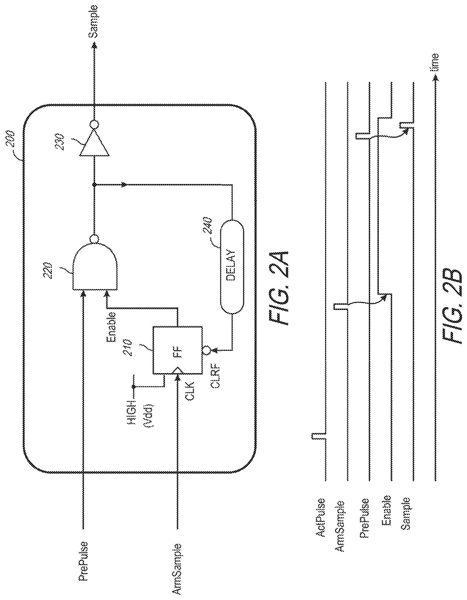
FIG. 2A depicts a circuit diagram a sampling circuit 200 in accordance with embodiments of the disclosure. The sampling circuit 200 may be the sampling circuit 160 in FIG. 1. The sampling circuit 200 may include a latch circuit 210 and a NAND circuit 220. For example, the latch circuit 210 may be a flip-flop that may receive the trigger signal for sampling (ArmSample) from the sampling timing generator circuit 120 at a clock input and a positive power potential (Vdd, a logic high level) at a data input and provide a latched ArmSample signal as an enable signal to the NAND circuit 220. The NAND circuit 220 may receive a PrePulse signal that may be active for one bank among a plurality of banks. The NAND circuit 220 may provide the latched ArmSample signal after inversion at an inverter 230 as a sampling signal (Sample), if the bank related to the received PrePulse signal is active. The latch circuit 210 may be reset by an inversion of the output signal of the NAND circuit 220 with a delay from a delay circuit 240.
FIG. 2B depicts a timing diagram of signals in the sampling circuit of FIG. 2A in accordance with embodiments of the present disclosure. Responsive to a pulse of an ActPulse signal, a pulse on the ArmSample signal is provided. The latch circuit 210 may provide an enable signal in an active state responsive to the pulse of the ArmSample signal. While the enable signal is in the active state, the NAND circuit 220 may provide a pulse on the Sample signal responsive to a pulse of the PrePulse signal.
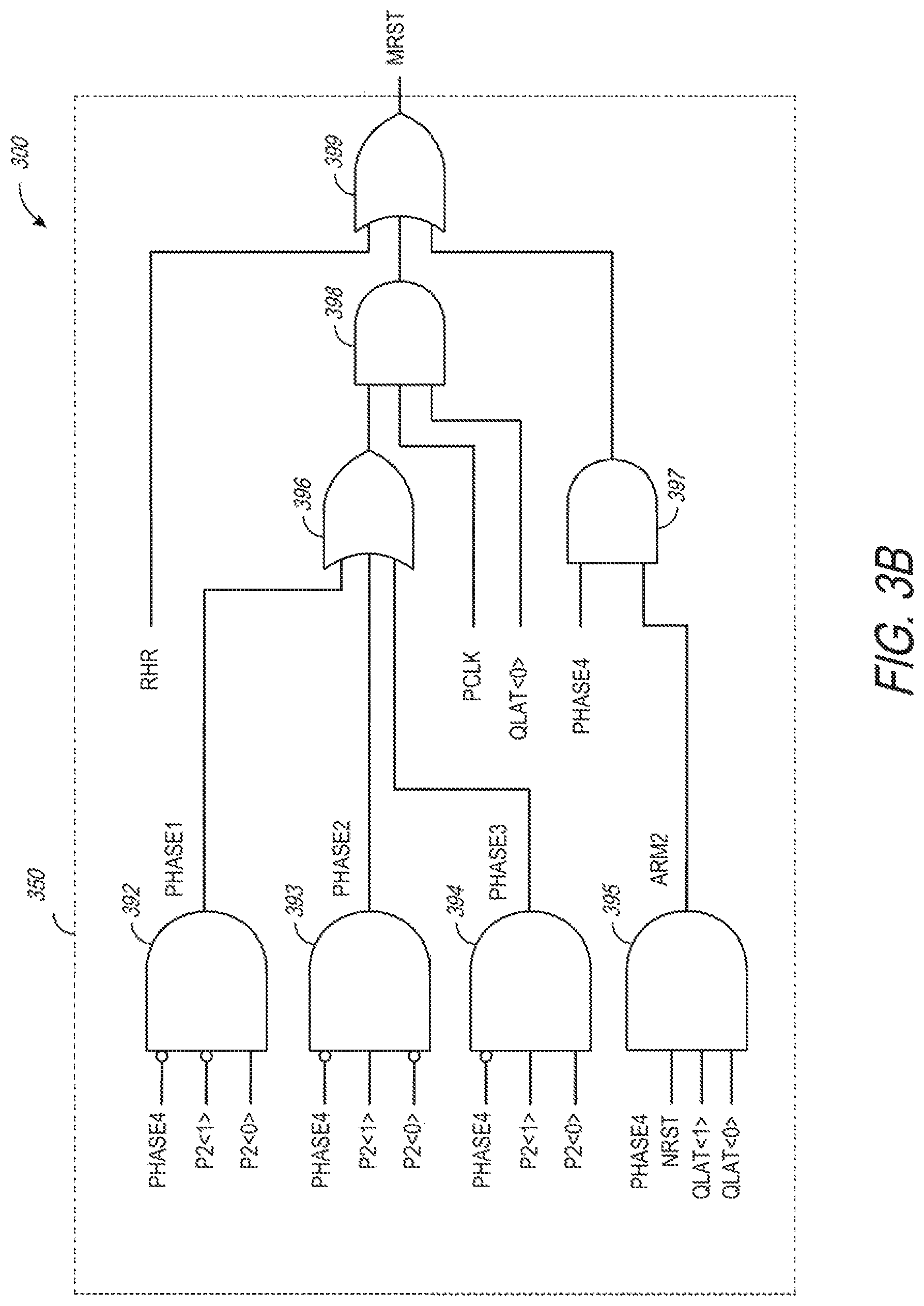
FIGS. 3A and 3B include a schematic diagram of a sampling timing generator circuit 300 and a RHR self-refresh oscillator circuit 301 in accordance with embodiments of the disclosure. For example, the sampling timing generator circuit 300 may be used as the sampling timing generator circuit 120 of FIG. 1 and the RHR self-refresh oscillator circuit 301 may be implemented in the RHR self-refresh oscillator circuit 140 of FIG. 1.
The RHR self-refresh oscillator circuit 301 may include a self-refresh oscillator 302 configured to provide an oscillation signal and a dock divider 304 that is configured to divide the oscillation signal by an X value to generate the RHROsc signal, wherein X is a positive integer value.
The sampling timing generator circuit 300 may include an interval circuit 310, a sampling trigger circuit 315, a secondary counter circuit 316, a counter reset circuit 350, and a randomized counter circuit 380. The interval circuit 310 may include a NAND gate 311, an OR gate 312, and an inverter 313. The NAND gate 311 is configured, to receive a steal slot signal and a refresh signal and to provide an inverted RHRF signal at an output based on the steal slot signal and the refresh signal. The inverter 313 is configured to invert the RHRF signal to provide the RHR signal, which may indicate an active RHR operation. The OR gate 312 is configured to receive an M-counter reset signal MRST and the RHRF signal, and to provide an N-counter clock latch signal NLATCLK based on the MRST and RHRF signals.
The sampling trigger circuit 315 includes circuitry that is configured to provide the ArmSample signal based on the RHROsc signal and the RHR signal. The sampling trigger circuit 315 includes an N-counter 320 coupled to a latch 330. The N-counter 320 may be a free running counter configured to count from zero to one less than a value of the NMAX signal in response to the RHROsc signal. In some examples, the N-counter 320 is a four bit counter. In some examples, the NMAX signal may be set to 9. The N-counter 320 provides an N<3:0> count value to the latch 330. In response to the NLATCLK signal from the interval circuit 310, the latch 330 may latch a value of the N<3:0> count as the NLAT<3:0> count value. An N-counter reset signal NRST may be set when the N<3:0> count value is equal to the NMAX value.
The sampling trigger circuit 315 may further include a M-counter 360 that is configured to toggle in response to an ArmSample signal to provide a M<3:0> count value. The NLAT<3:0> and the M<3:0> count values are compared at the comparator 370 to provide an inverse match signal MATCHF (e.g., the MATCHF signal is high when the NLAT<3:0> and the M<3:0> count values do not match). An AND gate 372 is configured to receive the MATCHF signal and the RHROsc signal and a delayed RHROsc signal via an inverter 371. An output of the AND gate 372 is provided to an OR gate 373, along with the ARM2 signal, and the OR gate 373 is configured to provide a control signal to the pulse generator 374 when either of the output of the AND gate 372 or the ARM2 signals are set.
The secondary counter circuit 316 includes a P1-counter 317, a P2-counter 318, and a flip-flop 319. The P1-counter 317 may include a free-running counter that continuously counts from zero to one less than the NMAX value in response to the RHROsc signal, and provides a pulse on a P-counter clock signal PCLK when the count value of the P1-counter 317 is equal to one less than the NMAX value. The P2-counter 318 is also a free-running counter that counts in response to the PCLK signal to provide a P2<2:0> count value at an output. The P1-counter 317 and the P2-counter 318 may be configured to be reset by the RHR signal form the interval circuit 310. In some examples, the P1-counter 317 is a four bit counter and the P2-counter 318 is a three bit counter. The flip-flop 319 is configured to set a PHASE4 signal to a high value in response to the P2<2> bit value toggling high.
The randomized counter circuit 380 is a randomized two bit counter circuit. The randomized counter circuit 380 includes a Q-counter 381, a Q-counter 382, and a latch 383. The Q-counter 381 is configured to toggle a Q<0> value in response to one of the RHROsc signal, an activate signal ACT, Or a Refresh signal. The Q-counter 382 is configured to toggle a Q<1> bit value in response to one of the RHROscF signal, the ACT signal, or the Refresh signal. The latch 383 is configured to latch the Q<1:0> count value in response to the NRST signal (e.g., when the N<3:0> count value is equal to one less than the NMAX value).
The counter reset circuit 350 includes an AND gate 392, an AND gate 393, an AND gate 394, configured to provide PHASE1, PHASE2, PHASE3 signals, respectively in response to values of the PHASE4 signal, and the P2<1> and P2<0> bit values. For example, the AND gate 392 is configured to set the PHASE1 signal when the PHASE4 signal and the P2<1> bit are not set and the P2<0> bit is set. The AND gate 393 is configured to set the PHASE2 signal when the PHASE4 signal and P2<0> bit are not set and the P2<1> bit is set. The AND gate 394 is configured to set the PHASE3 signal when the PHASE4 signal is not set and the P2<1> and P2<0> bits are set. If none of the PHASE1, PHASE2, PHASE3, and PHASE4 signals is set, then the sampling timing generator circuit 300 is in an initial phase e.g., PHASE0).
The counter reset circuit 350 further includes an AND gate 395 configured to set the ARM2 signal when the PHASE4, the NRST signals, and the bits of the QLAT<1:0> count values are all set. The OR gate 399 is configured to set the MRST signal when one of three conditions are met. First, the OR gate 399 is configured to set the MRST signal when the RHR signal is set (e.g., indicating a RHR event). Second, the OR gate 399 is configured to set the MRST signal when the PHASE4 and the ARM2 signals are set (e.g., via the AND gate 397). And lastly, the OR gate 399 is configured to set the MRST signal, via the AND gate 398, when the PCLK signal and QLAT<0> bit are set and any of the PHASE1, PHASE2, or PHASE3 signals is set (e.g., via the OR gate 396).
In operation, the RHR self-refresh oscillator circuit 301 is configured to provide the RHROsc signal, which is an oscillating signal that serves a counter clock for the N-counter 320, the Q-counter 381, and the Q-counter 382. The sampling timing generator circuit 300 is configured to trigger a sampling event via the ArmSample signal. Timing between RHR events (e.g., a RHR interval that is defined by consecutive pulses of the RHR signal) can be random, with some timing gaps significantly larger than others. Timing may be anticipated based on a count of clock cycles of the RHROsc signal, and the NMAX signal may be set to a value that is slightly larger than an anticipated RHR event gap. During this first or initial time period of an RHR interval, first circuitry (e.g., the N-counter 320, the latch 330, and the M-counter 360) may perform sampling operations within this 0 to NMAX sample time period. However, when the RHR interval is longer than the anticipated maximum, conventional timing-based RHR circuitry may have a gap where no sampling is being triggered by the ArmSample signal. This may pose a risk to a row hammer attack during these extended RHR intervals. To mitigate effects of these no sampling time periods, the sampling timing generator circuit 300 may implement second circuitry (e.g., the OR gate 312, secondary counter circuit 316, counter reset circuit 350, and randomized counter circuit 380) that is configured to initiate trigger of randomized sampling by the first circuitry during longer RHR intervals. The second circuitry delineates timing phases, from an initial time period PHASE0 (e.g., when the P2<2:0> count value is equal to 0), up to PHASE4 (e.g., when the PHASE4 signal is set (e.g., via the flip-flop 319). Each of the timing phases PHASE0-PHASE3 may have a duration of NMAX oscillations of the RHROsc signal. The PHASE4 time period may persist until the end of the RHR interval. The second circuitry may utilize a random QLAT<1:0> count value to randomly initiate a sampling event by the first circuitry.
During an initial phase or time period (e.g., PHASE0) of the RHR interval, the N-counter 320 repeatedly counts from 0 to one minus the NMAX value in response to the RHROsc signal. The latch 330 latches an N<3:0> count value in response to the NLATCLK signal to provide the NLAT<3:0> count value. The NLATCLK signal is set by the MRST signal or the RHRF signal. The MRST signal is set by the counter reset circuit 350 in response to an RHR signal (e.g., indicating initiation of a new RHR interval) or in a randomized fashion (e.g., based on a value of the randomized QLAT<1:0> bits) during one of the phases PHASE1-PHASE4. The NLAT<3:0> count value is compared with the M<3:0> count value of the M-counter 360. When the NLAT<3:0> count value and the M<3:0> count value do not match, the MATCHF signal is set. When the MATCHF signal is set, the AND gate 372 provides a pulse output in response to the RHROsc signal via the inverter 371, which causes the pulse generator 374 to provide a pulse on the ArmSample signal. The M-counter 360 increments the M<3:0> count in response to the pulses of the ArmSample signal. When there is a match between the NLAT<3:0> count value and the M<3:0> count value, the MATCHF signal is set low. In response to the MATCHF signal transitioning low, the AND gate 372 provides a continuous low output, and in response, the pulse generator 374 no longer provides pulse on the ArmSample signal. If the N-counter 320 and M-counter 360 were only reset at a start of the RHR interval via the RHR signal, during a long RHR interval that exceeds NMAX RHROsc oscillations, the sampling trigger circuit 315 would cease triggering sampling events via the ArmSample signal.
To mitigate this no sampling period during longer RHR intervals, the P1-counter 317 and the P2-counter 318 of the secondary counter circuit 316 may provide secondary counter circuitry that is used to track different phase time periods from PHASE0 (e.g., when the P2<2:0> count value is 0) up to PHASE4 (e.g., set via the flip-flop 319 in response to the P2<2> bit being set. The AND gate 392, the AND gate 393, and the AND gate 394 may set the PHASE1, PHASE2, and PHASE3 signals based on the PHASE4 signal and based on values of the P2<1:0> count values. For example, the AND gate 392 is configured to set the PHASE1 signal when the PHASE4 signal and P2<1> bit are not set and the P2<0> bit is set. The AND gate 393 is configured to set the PHASE2 signal when the PHASE4 signal and P2<0> bit are not set and the P2<1> bit is set. The AND gate 394 is configured to set the PHASE3 signal when the PHASE4 signal is not set and the P2<1> and P2<0> bits are set. If none of the PHASE1-PHASE4 signals are set, then the sampling trigger circuit 315 is operating in an initial time period PHASE0. The P1-counter 317 and the P2-counter 318 are reset in response to an RHR event (e.g., the RHR signal being set), which may move the circuitry of the sampling timing generator circuit 300 back to the initial phase PHASE0.
The QLAT<1:0> bits provided by the randomized counter circuit 380 may provide a randomized element to initiating new sampling events via the ArmSample signal during the time periods of PHASE1-PHASE4 (e.g., via the AND gate 395 for PHASE4, and via the OR gate 396 and the AND gate 398 for PHASE1, PHASE2, and PHASE3). That is, the ARM2 signal may be set during a PHASE4 time period in response to a pulse of the NRST signal when the QLAT<1:0> bits are both set. The MRST signal may be set to reset the latch 330 and M-counter 360 counters during any of the PHASE1 to PHASE3 time periods in response to a pulse on the PCLK signal when the QLAT<0> bit is set.
Together, the circuitry of the sampling timing generator circuit 300 provides sampling coverage for long RHR intervals, making a device less susceptible to a row hammer attack as compared with circuitry that has no sampling coverage for longer RHR intervals. It is appreciated that the number of bits in randomized counters may differ from shown without departing from the scope of the disclosure. For example, the N<3:0> (e.g., four bits), the NLAT<3:0> (e.g., four bits), the M<3:0> (e.g., four bits), the P2<2:0> (e.g., three bits) that count values of the N-counter 320, the latch 330, the M-counter 360, and the P2-counter 318, respectively, may include more or fewer than the number of bits shown. Additionally, implementations may include more than two random bits for the QLAT<1:0>. The logic of the 250 may use different combinations of the QLAT<1:0> bits to set the MRST signal. For example, the AND gate 398 may be configured to receive the QLAT<1> bit, rather than the QLAT<0> bit. Further, the AND gate 395 may be configured to receive an inverted value of at least one of the QLAT<1:0> bits.
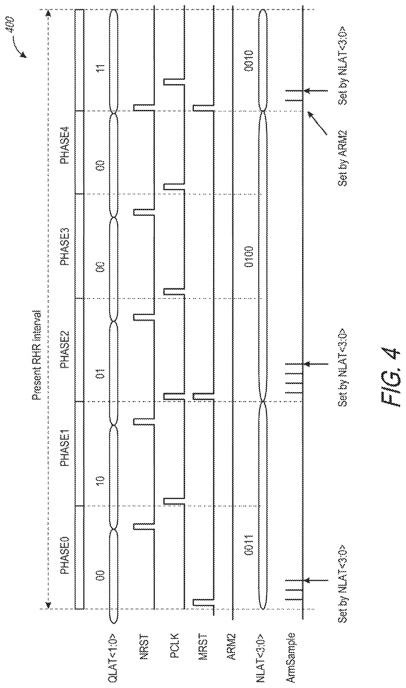
FIG. 4 depicts an exemplary timing diagram 400 associated with operation of a sampling timing generator circuit in accordance with embodiments of the disclosure. The timing diagram 400 may illustrate operation of the sampling timing generator circuit 120 of FIG. 1 and/or the sampling timing generator circuit 300 of FIGS. 3A and 3B. The QLAT<1:0> bits are a random signal that may correspond to the QLAT<1:0> bits of the randomized counter circuit 380 of FIG. 3A. The NRST signal may correspond to the NRST signal of the sampling trigger circuit 315 of FIG. 3A. The PCLK signal may correspond to the PCLK of the secondary counter circuit 316 of FIG. 3A. The MRST signal may correspond to the MRST signal of the interval circuit 310, the sampling trigger circuit 315, and the counter reset circuit 350 of FIGS. 3A and 3B. The ARM2 signal may correspond to the ARM2 signal of the sampling trigger circuit 315 and the counter reset circuit 350 of FIGS. 3A and 3B. The NLAT<3:0> may correspond to the NLAT<3:0> count value of the sampling trigger circuit 315 of FIG. 3A. The ArmSample signal may correspond to the ArmSample of the sampling timing generator circuit 120 of FIG. 1 and/or the ArmSample signal of the sampling trigger circuit 315 of FIG. 3A.
Because both the NRST and the PCLK signals are generated from counters (e.g., the N-counter 320 and the P1-counter 317, respectively, of FIG. 3A) controlled by oscillations of the RHROsc signal and both count from 0 to one minus the NMAX value, the time period between pulses on those signals are the same. The timing of the pulses may differ because the P1-counter is reset via the RHR signal, and the N-counter is never reset.
During the PHASE0 time period, in response to the pulse on the MRST signal, a latch (e.g., the latch 330 of FIG. 3A) may latch a new value for the NLAT<3:0> count value (e.g., the MRST signal pulse sets the NLATCLK signal via the OR gate 312 of FIG. 3A) and an M-counter (e.g., the M-counter 360 of FIG. 3A) is reset. In this example, the NLAT<3:0> count value is set to 3 (b0011). Because the M-counter is initialized to 0, the NLAT<3:0> count value does not match the M<3:0> count value. In response to the NLAT<3:0> count value not matching the M<3:0> count value, the MATCHF signal is set. In response to the MATCHF signal being set, the ArmSample signal is pulsed at a frequency equal to a frequency of the RHROsc signal (e.g., via the AND gate 372). With each pulse of the ArmSample signal, the M<3:0> count value is incremented. After 3 pulses (e.g., because the NLAT<3:0> count value is set to 3), the M<3:0> count value matches the NLAT<3:0> count value, and in response, the MATCHF signal is set low. In response to the MATCHF signal being set low, the pulses on the ArmSample signal stop (e.g., via the AND gate 372). The sampling timing generator circuit may remain in this state until the M-counter is reset via the MRST signal. In response to the pulse on the NRST signal, a new QLAT<1:0> count value of 2 (b10) is latched (e.g., via the latch 383 of FIG. 3A).
The sampling timing generator circuit may transition to PHASE1 in response to the PCLK signal (e.g., in response to an increment of the P2<2:0> count value from the P2-counter 318 to a value of 1). During the PHASE1 time period, no ArmSample signal pulses are provided because the M-counter signal is not reset via the MRST signal (e.g., the MRST signal remains low). The MRST signal may remain low because the QLAT<0> bit value is low (e.g., using the logic of the OR gate 396 and the AND gate 398 of the counter reset circuit 350 of FIG. 3B). In response to the pulse on the NRST signal, a new QLAT<1:0> count value of 1 (b01) is latched (e.g., via the latch 383 of FIG. 3A).
The sampling timing generator circuit may transition to PHASE2 in response to the PCLK signal (e.g., in response to an increment of the P2<2:0> count value from the P2-counter 318 to a value of 2). During the PHASE2 time period, in response to the QLAT<0> bit being set, a pulse may be provided on the MRST signal (e.g., using the logic of the OR gate 396, the AND gate 398, and the OR gate 399 of the counter reset circuit 350 of FIG. 3B). In response to the pulse on the MRST signal, the latch (e.g., the latch 330 of FIG. 3A) may latch a new value for the NLAT<3:0> count value (e.g., the MRST signal pulse sets the NLATCLK signal via the OR gate 312 of FIG. 3A) and an M-counter (e.g., the M-counter 360 of FIG. 3A) is reset. In this example, the NLAT<3:0> count value is set to 4 (b0100). Because the M-counter is initialized to 0, the NLAT<3:0> count value does not match the M<3:0> count value. In response to the NLAT<3:0> not matching the M<3:0> count value, the MATCHF signal is set. In response to the MATCHF signal being set, the ArmSample signal is pulsed at a frequency equal to a frequency of the RHROsc signal (e.g., via the AND gate 372). With each pulse of the ArmSample signal, the M<3:0> count is incremented. After 4 pulses (e.g., because NLAT<3:0> count value is set to 4), the M<3:0> count value matches the NLAT<3:0> count value, and in response, the MATCHF signal is set low. In response to the MATCHF signal being set low, the pulses on the ArmSample signal stop (e.g., via the AND gate 372). The sampling timing generator circuit may remain in this state until the M-counter is reset. In response to the pulse on the NRST signal, a new QLAT<1:0> count value of 0 (b00) is latched (e.g., via the latch 383 of FIG. 3A).
The sampling timing generator circuit may transition to PHASE3 in response to the PCLK signal (e.g., in response to an increment of the P2<2:0> count value from the P2-counter 318 to a value of 3). During the PHASE3 time period, no ArmSample signal pulses are provided because the M-counter signal is not reset via the MRST signal (e.g., the MRST signal remains low). The MRST signal may remain low because the QLAT<0> bit value is low (e.g., using the logic of the OR gate 396 and the AND gate 398 of the counter reset circuit 350 of FIG. 3B). In response to the pulse on the NRST signal, a new QLAT<1:0> count value of 0 (b00) is latched (e.g., via the latch 383 of FIG. 3A).
The sampling timing generator circuit may transition to PHASE4 in response to the PCLK signal (e.g., in response to an increment of the P2<2:0> count value from the P2-counter 318 to a value of 4, and in response to the interval circuit 310 latching the PHASE4 signal). The PHASE4 time period may persist until an RHR event (e.g., the RHR signal is set). During PHASE4, the MRST signal is set when the QLAT<1:0> value is 3 (b11) low (e.g., using the logic of the AND gate 395, the AND gate 397, and the OR gate 399 of the counter reset circuit 350 of FIG. 3B). Thus, while the QLAT<1:0> signal has a value of 0 (b00), no ArmSample signal pulses are generated. In response to the pulse on the NRST signal, a new QLAT<1:0> count value of 3 (b11) is latched (e.g., via the latch 383 of FIG. 3A). In response to the QLAT<1:0> value of 3 (b11), the ARM2 signal is set (e.g., using the AND gate 395 of FIG. 3B. In response to the ARM2 signal being set, the ArmSample signal is toggled (e.g., using the OR gate 373 and the pulse generator 374 of FIG. 3A), which may cause the M-counter to increment. In response to the M-counter incrementing, the MATCHF signal transitions high. Further, the MRST signal is pulsed while in PHASE4 when the ARM2 signal is set. In response to the pulse on the MRST signal, the latch (e.g., the latch 330 of FIG. 3A) may latch a new value for the NLAT<3:0> count value (e.g., the MRST signal pulse sets the NLATCLK signal via the OR gate 312 of FIG. 3A) and an M-counter (e.g., the M-counter 360 of FIG. 3A) is reset. In this example, the NLAT<3:0> count value is set to 2 (b0010). Because the M-counter is initialized to 0, the NLAT<3:0> count value does not match the M<3:0> count value. In response to the NLAT<3:0> not matching the M<3:0> count value, the MATCHF signal remains set. In response to the MATCHF signal being set, the ArmSample signal is pulsed at a frequency equal to a frequency of the RHROsc signal (e.g., via the AND gate 372). With each pulse of the ArmSample signal, the M<3:0> count is incremented. After 2 pulses (e.g., because NLAT<3:0> count value is set to 2), the M<3:0> count value matches the NLAT<3:0> count value, and in response, the MATCHF signal is set low. In response to the MATCHF signal being set low, the pulses on the ArmSample signal stop (e.g., via the AND gate 372). The sampling timing generator circuit may remain in this state until the M-counter is reset. In response to the pulse on the NRST signal, a new QLAT<1:0> count value of 0 (b00) is latched (e.g., via the latch 383 of FIG. 3A).
FIGS. 5A and 5B depict exemplary timing diagrams 500 and 501, respectively, associated with operation of a sampling timing generator circuit in accordance with embodiment of the disclosure. The timing diagram 500 may illustrate operation of the sampling timing generator circuit 120 of FIG. 1 and/or the sampling timing generator circuit 300 of FIGS. 3A and 3B. In particular, the timing diagrams 500 and 501 depict the impact of the random value of the QLAT<1:0> on whether the ArmSample signal triggers sampling events. The QLAT<1:0> bits are a random signal may correspond to the QLAT<1:0> signal of the randomized counter circuit 380 of FIG. 3A. The NRST signal may correspond to the NRST signal of the sampling trigger circuit 315 of FIG. 3A. The PCLK signal may correspond to the PCLK of the secondary counter circuit 316 of FIG. 3A. The MRST signal may correspond to the MRST signal of the interval circuit 310, the sampling trigger circuit 315, and the counter reset circuit 350 of FIGS. 3A and 3B. The ARM2 signal may correspond to the ARM2 signal of the sampling trigger circuit 315 and the counter reset circuit 350 of FIGS. 3A and 3B. The NLAT<3:0> may correspond to the NLAT<3:0> count value of the sampling trigger circuit 315 of FIG. 3A. The ArmSample signal may correspond to the ArmSample of the sampling timing generator circuit 120 of FIG. 1 and/or the ArmSample signal of the sampling trigger circuit 315 of FIG. 3A.
Because both the NRST and the PCLK signals are generated from counters (e.g., the N-counter 320 and the P1-counter 317, respectively, of FIG. 3A) controlled by oscillations of the RHROsc signal and both count from 0 to one minus the NMAX value, the time period between pulses on those signals are the same. The timing of the pulses may differ because the P1-counter is reset via the RHR signal, and the N-counter is never reset.
Referring to both of the timing diagrams 500 and 501, during the PHASE0 time period, in response to the pulse on the MRST signal, a latch (e.g., the latch 330 of FIG. 3A) may latch a new value for the NLAT<3:0> count value (e.g., the MRST signal pulse sets the NLATCLK signal via the OR gate 312 of FIG. 3A) and an M-counter (e.g., the M-counter 360 of FIG. 3A) is reset. In this example, the NLAT<3:0> count value is set to 3 (b0011). Because the M-counter is initialized to 0, the NLAT<3:0> count value does not match the M<3:0> count value. In response to the NLAT<3:0> count value not matching the M<3:0> count value, the MATCHF signal is set. In response to the MATCHF signal being set, the ArmSample signal is pulsed at a frequency equal to a frequency of the RHROsc signal (e.g., via the AND gate 372). With each pulse of the ArmSample signal, the M<3:0> count value is incremented. After 3 pulses (e.g., because the NLAT<3:0> count value is set to 3), the M<3:0> count value matches the NLAT<3:0> count value, and in response, the MATCHF signal is set low. In response to the MATCHF signal being set low, the pulses on the ArmSample signal stop (e.g., via the AND gate 372). The sampling timing generator circuit may remain in this state until the M-counter is reset via the MRST signal.
For the timing diagram 500, in response to the pulse on the NRST signal, a new QLAT<1:0> count value of 2 (b10) is latched (e.g., via the latch 383 of FIG. 3A). For the timing diagram 501, in response to the pulse on the NRST signal, a new QLAT<1:0> count value of 1 (b10) is latched (e.g., via the latch 383 of FIG. 3A). Because the QLAT<0> value is used to determine whether the MRST signal is set during PHASE1 to PHASE3 (e.g., using the AND gate 398 of the counter reset circuit 350 of FIG. 3B), the timing diagrams 500 and 501 operate differently.
In the timing diagram 500, the sampling timing generator circuit may transition to PHASE1 in response to the PCLK signal (e.g., in response to an increment of the P2<2:0> count value from the P2-counter 318 to a value of 1). During the PHASE1 time period, no ArmSample signal pulses are provided because the M-counter signal is not reset via the MRST signal (e.g., the MRST signal remains low). The MRST signal may remain low because the QLAT<0> bit value is low (e.g., using the logic of the OR gate 396 and the AND gate 398 of the counter reset circuit 350 of FIG. 3B).
In the timing diagram 501, in response to the QLAT<0> bit being set, a pulse may be provided on the MRST signal (e.g., using the logic of the OR gate 396, the AND gate 398, and the OR gate 399 of the counter reset circuit 350 of FIG. 3B). In response to the pulse on the MRST signal, the latch (e.g., the latch 330 of FIG. 3A) may latch a new value for the NLAT<3:0> count value (e.g., the MRST signal pulse sets the NLATCLK signal via the OR gate 312 of FIG. 3A) and an M-counter (e.g., the M-counter 360 of FIG. 3A) is reset. In this example, the NLAT<3:0> count value is set to 2 (b0010). Because the M-counter is initialized to 0, the NLAT<3:0> count value does not match the M<3:0> count value. In response to the NLAT<3:0> not matching the M<3:0> count value, the MATCHF signal is set. In response to the MATCHF signal being set, the ArmSample signal is pulsed at a frequency equal to a frequency of the RHROsc signal (e.g., via the AND gate 372). With each pulse of the ArmSample signal, the M<3:0> count is incremented. After 2 pulses (e.g., because NLAT<3:0> count value is set to 2), the M<3:0> count value matches the NLAT<3:0> count value, and in response, the MATCHF signal is set low. In response to the MATCHF signal being set low, the pulses on the ArmSample signal stop (e.g., via the AND gate 372). The sampling timing generator circuit may remain in this state until the M-counter is reset.
The timing diagram 400 of FIG. 4 and the timing diagrams 500 and 501 of FIGS. 5A and 5B, respectively are exemplary. Relative timing may differ in different implementations, and the latched values of various signals may differ from depicted. Specifically, the NLAT<3:0> and QLAT<1:0> count values are intended to be random based on a time at which they are latched.
Logic levels of signals, types of transistors, types of data input circuits used in the embodiments described the above are merely examples. However, in other embodiments, combinations of the logic levels of signals, types of transistors, types of data input circuits other than those specifically described in the present disclosure may be used without departing from the scope of the present disclosure.
Although various embodiments of the disclosure have been disclosed, it will be understood by those skilled in the art that the scope of the disclosure extends beyond the specifically disclosed embodiments to other alternative embodiments and/or uses and obvious modifications and equivalents thereof. In addition, other modifications which are within the scope of the disclosure will be readily apparent to those of skill in the art. It is also contemplated that various combination or sub-combination of the specific features and aspects of the embodiments may be made and still fall within the scope of the disclosure. It should be understood that various features and aspects of the disclosed embodiments can be combined with or substituted for one another in order to form alternative embodiments of the disclosure. Thus, it is intended that the scope of at least some of the disclosure should not be limited by the particular disclosed embodiments described above.
* * * * *
D00000
D00001
D00002
D00003
D00004
D00005
D00006
XML
uspto.report is an independent third-party trademark research tool that is not affiliated, endorsed, or sponsored by the United States Patent and Trademark Office (USPTO) or any other governmental organization. The information provided by uspto.report is based on publicly available data at the time of writing and is intended for informational purposes only.
While we strive to provide accurate and up-to-date information, we do not guarantee the accuracy, completeness, reliability, or suitability of the information displayed on this site. The use of this site is at your own risk. Any reliance you place on such information is therefore strictly at your own risk.
All official trademark data, including owner information, should be verified by visiting the official USPTO website at www.uspto.gov. This site is not intended to replace professional legal advice and should not be used as a substitute for consulting with a legal professional who is knowledgeable about trademark law.