3D semiconductor device and structure
Or-Bach , et al. June 1, 2
U.S. patent number 11,024,673 [Application Number 17/121,741] was granted by the patent office on 2021-06-01 for 3d semiconductor device and structure. This patent grant is currently assigned to Monolithic 3D Inc.. The grantee listed for this patent is Monolithic 3D Inc.. Invention is credited to Brian Cronquist, Zvi Or-Bach, Deepak C. Sekar.


View All Diagrams
| United States Patent | 11,024,673 |
| Or-Bach , et al. | June 1, 2021 |
3D semiconductor device and structure
Abstract
A 3D semiconductor device, the device including: a first level including a single crystal layer, a first metal layer, a second metal layer above the first metal layer, and a third metal layer above the second metal layer, where the second metal layer is significantly thicker than either the third metal layer or the first metal layer, where the third metal layer is precisely aligned to the first metal layer with less than 20 nm misalignment; a second level including a first array of first memory cells, each of the first memory cells include first transistors; a third level including a second array of second memory cells, each of the second memory cells include second transistors, where the second level is above the third level, where the second transistors are self-aligned to the first transistors, being processed following the same lithography step; and periphery circuits connected by the second metal to control the memory cells, where the periphery circuits are either underneath or atop the memory cells.
| Inventors: | Or-Bach; Zvi (Haifa, IL), Sekar; Deepak C. (Sunnyvale, CA), Cronquist; Brian (Klamath Falls, OR) | ||||||||||
|---|---|---|---|---|---|---|---|---|---|---|---|
| Applicant: |
|
||||||||||
| Assignee: | Monolithic 3D Inc. (Klamath
Falls, OR) |
||||||||||
| Family ID: | 1000005591347 | ||||||||||
| Appl. No.: | 17/121,741 | ||||||||||
| Filed: | December 14, 2020 |
Related U.S. Patent Documents
| Application Number | Filing Date | Patent Number | Issue Date | ||
|---|---|---|---|---|---|
| 17114155 | Dec 7, 2020 | ||||
| 17013823 | Sep 7, 2020 | 10825864 | |||
| 16409813 | Nov 3, 2020 | 10825864 | |||
| 15803732 | May 14, 2019 | 10290682 | |||
| 14555494 | Nov 14, 2017 | 9818800 | |||
| 13246157 | Feb 17, 2015 | 8956959 | |||
| 13173999 | Jun 19, 2012 | 8203148 | |||
| 12901890 | Sep 27, 2011 | 8026521 | |||
| Current U.S. Class: | 1/1 |
| Current CPC Class: | H01L 21/84 (20130101); H01L 27/11 (20130101); H01L 27/10897 (20130101); H01L 27/228 (20130101); H01L 21/268 (20130101); H01L 21/845 (20130101); H01L 27/11551 (20130101); H01L 27/11529 (20130101); H01L 27/2436 (20130101); H01L 27/1203 (20130101); H01L 27/1211 (20130101); H01L 29/7841 (20130101); H01L 27/2481 (20130101); H01L 29/785 (20130101); H01L 21/76254 (20130101); H01L 27/11578 (20130101); H01L 27/10802 (20130101); H01L 29/42392 (20130101); H01L 21/8221 (20130101); H01L 27/249 (20130101); H01L 27/0688 (20130101); H01L 21/6835 (20130101); H01L 27/10826 (20130101); H01L 2221/6835 (20130101); H01L 2029/7857 (20130101); H01L 27/105 (20130101); H01L 45/1226 (20130101); H01L 27/11573 (20130101); H01L 45/04 (20130101); H01L 45/146 (20130101); H01L 27/11526 (20130101); H01L 27/10879 (20130101) |
| Current International Class: | H01L 21/683 (20060101); H01L 21/822 (20060101); H01L 27/06 (20060101); H01L 21/762 (20060101); H01L 27/24 (20060101); H01L 27/108 (20060101); H01L 27/22 (20060101); H01L 27/12 (20060101); H01L 27/11578 (20170101); H01L 21/268 (20060101); H01L 29/423 (20060101); H01L 27/11551 (20170101); H01L 29/78 (20060101); H01L 27/11529 (20170101); H01L 27/11 (20060101); H01L 21/84 (20060101); H01L 27/105 (20060101); H01L 27/11526 (20170101); H01L 27/11573 (20170101); H01L 45/00 (20060101) |
| Field of Search: | ;257/202,288,500 |
References Cited [Referenced By]
U.S. Patent Documents
| 3007090 | October 1961 | Rutz |
| 3819959 | June 1974 | Chang et al. |
| 4009483 | February 1977 | Clark |
| 4197555 | April 1980 | Uehara et al. |
| 4213139 | July 1980 | Rao et al. |
| 4400715 | August 1983 | Barbee et al. |
| 4487635 | December 1984 | Kugimiya et al. |
| 4510670 | April 1985 | Schwabe |
| 4522657 | June 1985 | Rohatgi et al. |
| 4612083 | September 1986 | Yasumoto et al. |
| 4643950 | February 1987 | Ogura et al. |
| 4704785 | November 1987 | Curran |
| 4711858 | December 1987 | Harder et al. |
| 4721885 | January 1988 | Brodie |
| 4732312 | March 1988 | Kennedy et al. |
| 4733288 | March 1988 | Sato |
| 4829018 | May 1989 | Wahlstrom |
| 4854986 | August 1989 | Raby |
| 4866304 | September 1989 | Yu |
| 4939568 | July 1990 | Kato et al. |
| 4956307 | September 1990 | Pollack et al. |
| 5012153 | April 1991 | Atkinson et al. |
| 5032007 | July 1991 | Silverstein et al. |
| 5047979 | September 1991 | Leung |
| 5087585 | February 1992 | Hayashi |
| 5093704 | March 1992 | Sato et al. |
| 5106775 | April 1992 | Kaga et al. |
| 5152857 | October 1992 | Ito et al. |
| 5162879 | November 1992 | Gill |
| 5189500 | February 1993 | Kusunoki |
| 5217916 | June 1993 | Anderson et al. |
| 5250460 | October 1993 | Yamagata et al. |
| 5258643 | November 1993 | Cohen |
| 5265047 | November 1993 | Leung et al. |
| 5266511 | November 1993 | Takao |
| 5277748 | January 1994 | Sakaguchi et al. |
| 5286670 | February 1994 | Kang et al. |
| 5294556 | March 1994 | Kawamura |
| 5308782 | May 1994 | Mazure et al. |
| 5312771 | May 1994 | Yonehara |
| 5317236 | May 1994 | Zavracky et al. |
| 5324980 | June 1994 | Kusunoki |
| 5355022 | October 1994 | Sugahara et al. |
| 5371037 | December 1994 | Yonehara |
| 5374564 | December 1994 | Bruel |
| 5374581 | December 1994 | Ichikawa et al. |
| 5424560 | June 1995 | Norman et al. |
| 5475280 | December 1995 | Jones et al. |
| 5478762 | December 1995 | Chao |
| 5485031 | January 1996 | Zhang et al. |
| 5498978 | March 1996 | Takahashi et al. |
| 5527423 | June 1996 | Neville et al. |
| 5535342 | July 1996 | Taylor |
| 5554870 | September 1996 | Fitch et al. |
| 5563084 | October 1996 | Ramm et al. |
| 5583349 | December 1996 | Norman et al. |
| 5583350 | December 1996 | Norman et al. |
| 5586291 | December 1996 | Lasker |
| 5594563 | January 1997 | Larson |
| 5604137 | February 1997 | Yamazaki et al. |
| 5617991 | April 1997 | Pramanick et al. |
| 5627106 | May 1997 | Hsu |
| 5656548 | August 1997 | Zavracky et al. |
| 5656553 | August 1997 | Leas et al. |
| 5659194 | August 1997 | Iwamatsu |
| 5670411 | September 1997 | Yonehara |
| 5681756 | October 1997 | Norman et al. |
| 5695557 | December 1997 | Yamagata et al. |
| 5701027 | December 1997 | Gordon et al. |
| 5707745 | January 1998 | Forrest et al. |
| 5714395 | February 1998 | Bruel |
| 5721160 | February 1998 | Forrest et al. |
| 5737748 | April 1998 | Shigeeda |
| 5739552 | April 1998 | Kimura et al. |
| 5744979 | April 1998 | Goetting |
| 5748161 | May 1998 | Lebby et al. |
| 5757026 | May 1998 | Forrest et al. |
| 5770483 | June 1998 | Kadosh |
| 5770881 | June 1998 | Pelella et al. |
| 5781031 | July 1998 | Bertin et al. |
| 5817574 | October 1998 | Gardner |
| 5829026 | October 1998 | Leung et al. |
| 5835396 | November 1998 | Zhang |
| 5854123 | December 1998 | Sato et al. |
| 5861929 | January 1999 | Spitzer |
| 5877034 | March 1999 | Ramm |
| 5877070 | March 1999 | Goesele et al. |
| 5882987 | March 1999 | Srikrishnan |
| 5883525 | March 1999 | Tavana et al. |
| 5889903 | March 1999 | Rao |
| 5893721 | April 1999 | Huang et al. |
| 5915167 | June 1999 | Leedy |
| 5920788 | July 1999 | Reinberg |
| 5937312 | August 1999 | Iyer et al. |
| 5943574 | August 1999 | Tehrani et al. |
| 5952680 | September 1999 | Strife |
| 5952681 | September 1999 | Chen |
| 5965875 | October 1999 | Merrill |
| 5977579 | November 1999 | Noble |
| 5977961 | November 1999 | Rindal |
| 5980633 | November 1999 | Yamagata et al. |
| 5985742 | November 1999 | Henley et al. |
| 5994746 | November 1999 | Reisinger |
| 5998808 | December 1999 | Matsushita |
| 6001693 | December 1999 | Yeouchung et al. |
| 6009496 | December 1999 | Tsai |
| 6020252 | February 2000 | Aspar et al. |
| 6020263 | February 2000 | Shih et al. |
| 6027958 | February 2000 | Vu et al. |
| 6030700 | February 2000 | Forrest et al. |
| 6052498 | April 2000 | Paniccia |
| 6054370 | April 2000 | Doyle |
| 6057212 | May 2000 | Chan et al. |
| 6071795 | June 2000 | Cheung et al. |
| 6075268 | June 2000 | Gardner et al. |
| 6103597 | August 2000 | Aspar et al. |
| 6111260 | August 2000 | Dawson et al. |
| 6125217 | September 2000 | Paniccia et al. |
| 6153495 | November 2000 | Kub et al. |
| 6191007 | February 2001 | Matsui et al. |
| 6200878 | March 2001 | Yamagata |
| 6222203 | April 2001 | Ishibashi et al. |
| 6226197 | May 2001 | Nishimura |
| 6229161 | May 2001 | Nemati et al. |
| 6242324 | June 2001 | Kub et al. |
| 6242778 | June 2001 | Marmillion et al. |
| 6252465 | June 2001 | Katoh |
| 6259623 | July 2001 | Takahashi |
| 6261935 | July 2001 | See et al. |
| 6264805 | July 2001 | Forrest et al. |
| 6281102 | August 2001 | Cao et al. |
| 6294018 | September 2001 | Hamm et al. |
| 6306705 | October 2001 | Parekh et al. |
| 6321134 | November 2001 | Henley et al. |
| 6322903 | November 2001 | Siniaguine et al. |
| 6331468 | December 2001 | Aronowitz et al. |
| 6331790 | December 2001 | Or-Bach et al. |
| 6331943 | December 2001 | Naji et al. |
| 6353492 | March 2002 | McClelland et al. |
| 6355501 | March 2002 | Fung et al. |
| 6355976 | March 2002 | Faris |
| 6358631 | March 2002 | Forrest et al. |
| 6365270 | April 2002 | Forrest et al. |
| 6376337 | April 2002 | Wang et al. |
| 6377504 | April 2002 | Hilbert |
| 6380046 | April 2002 | Yamazaki |
| 6392253 | May 2002 | Saxena |
| 6404043 | June 2002 | Isaak |
| 6417108 | July 2002 | Akino et al. |
| 6420215 | July 2002 | Knall et al. |
| 6423614 | July 2002 | Doyle |
| 6429481 | August 2002 | Mo et al. |
| 6429484 | August 2002 | Yu |
| 6430734 | August 2002 | Zahar |
| 6448615 | September 2002 | Forbes |
| 6475869 | November 2002 | Yu |
| 6476493 | November 2002 | Or-Bach et al. |
| 6479821 | November 2002 | Hawryluk et al. |
| 6483707 | November 2002 | Freuler et al. |
| 6507115 | January 2003 | Hofstee |
| 6515334 | February 2003 | Yamazaki et al. |
| 6515511 | February 2003 | Sugibayashi et al. |
| 6526559 | February 2003 | Schiefele et al. |
| 6528391 | March 2003 | Henley et al. |
| 6534352 | March 2003 | Kim |
| 6534382 | March 2003 | Sakaguchi et al. |
| 6544837 | April 2003 | Divakauni et al. |
| 6545314 | April 2003 | Forbes et al. |
| 6555901 | April 2003 | Yoshihara et al. |
| 6563139 | May 2003 | Hen |
| 6580124 | June 2003 | Cleeves |
| 6580289 | June 2003 | Cox |
| 6600173 | July 2003 | Tiwari |
| 6617694 | September 2003 | Kodaira et al. |
| 6620659 | September 2003 | Emmma et al. |
| 6624046 | September 2003 | Zavracky et al. |
| 6627518 | September 2003 | Inoue et al. |
| 6627985 | September 2003 | Huppenthal et al. |
| 6630713 | October 2003 | Geusic |
| 6635552 | October 2003 | Gonzalez |
| 6635588 | October 2003 | Hawryluk et al. |
| 6638834 | October 2003 | Gonzalez |
| 6642744 | November 2003 | Or-Bach et al. |
| 6653209 | November 2003 | Yamagata |
| 6653712 | November 2003 | Knall et al. |
| 6661085 | December 2003 | Kellar et al. |
| 6677204 | January 2004 | Cleeves et al. |
| 6686253 | February 2004 | Or-Bach |
| 6689660 | February 2004 | Noble |
| 6701071 | March 2004 | Wada et al. |
| 6703328 | March 2004 | Tanaka et al. |
| 6756633 | June 2004 | Wang et al. |
| 6756811 | June 2004 | Or-Bach |
| 6759282 | July 2004 | Campbell et al. |
| 6762076 | July 2004 | Kim et al. |
| 6774010 | August 2004 | Chu et al. |
| 6805979 | October 2004 | Ogura et al. |
| 6806171 | October 2004 | Ulyashin et al. |
| 6809009 | October 2004 | Aspar et al. |
| 6815781 | November 2004 | Vyvoda et al. |
| 6819136 | November 2004 | Or-Bach |
| 6821826 | November 2004 | Chan et al. |
| 6841813 | January 2005 | Walker et al. |
| 6844243 | January 2005 | Gonzalez |
| 6864534 | March 2005 | Ipposhi et al. |
| 6875671 | April 2005 | Faris |
| 6882572 | April 2005 | Wang et al. |
| 6888375 | May 2005 | Feng et al. |
| 6917219 | July 2005 | New |
| 6927431 | August 2005 | Gonzalez |
| 6930511 | August 2005 | Or-Bach |
| 6943067 | September 2005 | Greenlaw |
| 6943407 | September 2005 | Ouyang et al. |
| 6949421 | September 2005 | Padmanabhan et al. |
| 6953956 | October 2005 | Or-Bach et al. |
| 6967149 | November 2005 | Meyer et al. |
| 6985012 | January 2006 | Or-Bach |
| 6989687 | January 2006 | Or-Bach |
| 6995430 | February 2006 | Langdo et al. |
| 6995456 | February 2006 | Nowak |
| 7015719 | March 2006 | Feng et al. |
| 7016569 | March 2006 | Mule et al. |
| 7018875 | March 2006 | Madurawe |
| 7019557 | March 2006 | Madurawe |
| 7043106 | May 2006 | West et al. |
| 7052941 | May 2006 | Lee |
| 7064579 | June 2006 | Madurawe |
| 7067396 | June 2006 | Aspar et al. |
| 7067909 | June 2006 | Reif et al. |
| 7068070 | June 2006 | Or-Bach |
| 7068072 | June 2006 | New et al. |
| 7078739 | July 2006 | Nemati et al. |
| 7094667 | August 2006 | Bower |
| 7098691 | August 2006 | Or-Bach et al. |
| 7105390 | September 2006 | Brask et al. |
| 7105871 | September 2006 | Or-Bach et al. |
| 7109092 | September 2006 | Tong |
| 7110629 | September 2006 | Bjorkman et al. |
| 7111149 | September 2006 | Eilert |
| 7112815 | September 2006 | Prall |
| 7115945 | October 2006 | Lee et al. |
| 7115966 | October 2006 | Ido et al. |
| 7141853 | November 2006 | Campbell et al. |
| 7148119 | December 2006 | Sakaguchi et al. |
| 7157787 | January 2007 | Kim et al. |
| 7157937 | January 2007 | Apostol et al. |
| 7166520 | January 2007 | Henley |
| 7170807 | January 2007 | Fazan et al. |
| 7173369 | February 2007 | Forrest et al. |
| 7180091 | February 2007 | Yamazaki et al. |
| 7180379 | February 2007 | Hopper et al. |
| 7183611 | February 2007 | Bhattacharyya |
| 7189489 | March 2007 | Kunimoto et al. |
| 7205204 | April 2007 | Ogawa et al. |
| 7209384 | April 2007 | Kim |
| 7217636 | May 2007 | Atanackovic |
| 7223612 | May 2007 | Sarma |
| 7242012 | July 2007 | Leedy |
| 7245002 | July 2007 | Akino et al. |
| 7256104 | August 2007 | Ito et al. |
| 7259091 | August 2007 | Schuehrer et al. |
| 7265421 | September 2007 | Madurawe |
| 7271420 | September 2007 | Cao |
| 7274207 | September 2007 | Sugawara et al. |
| 7282951 | October 2007 | Huppenthal et al. |
| 7284226 | October 2007 | Kondapalli |
| 7296201 | November 2007 | Abramovici |
| 7304355 | December 2007 | Zhang |
| 7312109 | December 2007 | Madurawe |
| 7312487 | December 2007 | Alam et al. |
| 7314788 | January 2008 | Shaw |
| 7335573 | February 2008 | Takayama et al. |
| 7337425 | February 2008 | Kirk |
| 7338884 | March 2008 | Shimoto et al. |
| 7342415 | March 2008 | Teig et al. |
| 7351644 | April 2008 | Henley |
| 7358601 | April 2008 | Plants et al. |
| 7362133 | April 2008 | Madurawe |
| 7369435 | May 2008 | Forbes |
| 7371660 | May 2008 | Henley et al. |
| 7378702 | May 2008 | Lee |
| 7381989 | June 2008 | Kim |
| 7385283 | June 2008 | Wu |
| 7393722 | July 2008 | Issaq et al. |
| 7402483 | July 2008 | Yu et al. |
| 7402897 | July 2008 | Leedy |
| 7419844 | September 2008 | Lee et al. |
| 7432185 | October 2008 | Kim |
| 7436027 | October 2008 | Ogawa et al. |
| 7439773 | October 2008 | Or-Bach et al. |
| 7446563 | November 2008 | Madurawe |
| 7459752 | December 2008 | Doris et al. |
| 7459763 | December 2008 | Issaq et al. |
| 7459772 | December 2008 | Speers |
| 7463062 | December 2008 | Or-Bach et al. |
| 7463502 | December 2008 | Stipe |
| 7470142 | December 2008 | Lee |
| 7470598 | December 2008 | Lee |
| 7476939 | January 2009 | Okhonin et al. |
| 7477540 | January 2009 | Okhonin et al. |
| 7485968 | February 2009 | Enquist et al. |
| 7486563 | February 2009 | Waller et al. |
| 7488980 | February 2009 | Takafuji et al. |
| 7492632 | February 2009 | Carman |
| 7495473 | February 2009 | McCollum et al. |
| 7498675 | March 2009 | Farnworth et al. |
| 7499352 | March 2009 | Singh |
| 7499358 | March 2009 | Bauser |
| 7508034 | March 2009 | Takafuji et al. |
| 7514748 | April 2009 | Fazan et al. |
| 7521806 | April 2009 | Trezza |
| 7525186 | April 2009 | Kim et al. |
| 7535089 | May 2009 | Fitzgerald |
| 7541616 | June 2009 | Fazan et al. |
| 7547589 | June 2009 | Iriguchi |
| 7553745 | June 2009 | Lim |
| 7557367 | July 2009 | Rogers et al. |
| 7558141 | July 2009 | Katsumata et al. |
| 7563659 | July 2009 | Kwon et al. |
| 7566855 | July 2009 | Olsen et al. |
| 7566974 | July 2009 | Konevecki |
| 7586778 | September 2009 | Ho et al. |
| 7589375 | September 2009 | Jang |
| 7608848 | October 2009 | Ho et al. |
| 7612411 | November 2009 | Walker |
| 7615462 | November 2009 | Kim et al. |
| 7622367 | November 2009 | Nuzzo et al. |
| 7632738 | December 2009 | Lee |
| 7633162 | December 2009 | Lee |
| 7666723 | February 2010 | Frank et al. |
| 7670912 | March 2010 | Yeo |
| 7671371 | March 2010 | Lee |
| 7671460 | March 2010 | Lauxtermann et al. |
| 7674687 | March 2010 | Henley |
| 7687372 | March 2010 | Jain |
| 7687872 | March 2010 | Cazaux |
| 7688619 | March 2010 | Lung et al. |
| 7692202 | April 2010 | Bensch |
| 7692448 | April 2010 | Solomon |
| 7692944 | April 2010 | Bernstein et al. |
| 7697316 | April 2010 | Lai et al. |
| 7709932 | May 2010 | Nemoto et al. |
| 7718508 | May 2010 | Lee |
| 7719876 | May 2010 | Chevallier |
| 7723207 | May 2010 | Alam et al. |
| 7728326 | June 2010 | Yamazaki et al. |
| 7732301 | June 2010 | Pinnington et al. |
| 7741673 | June 2010 | Tak et al. |
| 7742331 | June 2010 | Watanabe |
| 7745250 | June 2010 | Han |
| 7749884 | July 2010 | Mathew et al. |
| 7750669 | July 2010 | Spangaro |
| 7755622 | July 2010 | Yvon |
| 7759043 | July 2010 | Tanabe et al. |
| 7768115 | August 2010 | Lee et al. |
| 7772039 | August 2010 | Kerber |
| 7772096 | August 2010 | DeSouza et al. |
| 7774735 | August 2010 | Sood |
| 7776715 | August 2010 | Wells et al. |
| 7777330 | August 2010 | Pelley et al. |
| 7786460 | August 2010 | Lung et al. |
| 7786535 | August 2010 | Abou-Khalil et al. |
| 7790524 | September 2010 | Abadeer et al. |
| 7795619 | September 2010 | Hara |
| 7799675 | September 2010 | Lee |
| 7800099 | September 2010 | Yamazaki et al. |
| 7800148 | September 2010 | Lee et al. |
| 7800163 | September 2010 | Izumi et al. |
| 7800199 | September 2010 | Oh et al. |
| 7816721 | October 2010 | Yamazaki |
| 7843718 | November 2010 | Koh et al. |
| 7846814 | December 2010 | Lee |
| 7863095 | January 2011 | Sasaki et al. |
| 7864568 | January 2011 | Fujisaki et al. |
| 7867822 | January 2011 | Lee |
| 7888764 | February 2011 | Lee |
| 7910432 | March 2011 | Tanaka et al. |
| 7915164 | March 2011 | Konevecki et al. |
| 7919845 | April 2011 | Karp |
| 7965102 | June 2011 | Bauer et al. |
| 7968965 | June 2011 | Kim |
| 7969193 | June 2011 | Wu et al. |
| 7973314 | July 2011 | Yang |
| 7982250 | July 2011 | Yamazaki et al. |
| 7983065 | July 2011 | Samachisa |
| 8008732 | August 2011 | Kiyotoshi |
| 8013399 | September 2011 | Thomas et al. |
| 8014166 | September 2011 | Yazdani |
| 8014195 | September 2011 | Okhonin et al. |
| 8022493 | September 2011 | Bang |
| 8030780 | October 2011 | Kirby et al. |
| 8031544 | October 2011 | Kim et al. |
| 8032857 | October 2011 | McIlrath |
| 8044448 | October 2011 | Kamigaichi et al. |
| 8044464 | October 2011 | Yamazaki et al. |
| 8068364 | November 2011 | Maejima |
| 8106520 | January 2012 | Keeth et al. |
| 8107276 | January 2012 | Breitwisch et al. |
| 8129256 | March 2012 | Farooq et al. |
| 8129258 | March 2012 | Hosier et al. |
| 8130547 | March 2012 | Wiidjaja et al. |
| 8136071 | March 2012 | Solomon |
| 8138502 | March 2012 | Nakamura et al. |
| 8153520 | April 2012 | Chandrashekar |
| 8158515 | April 2012 | Farooq et al. |
| 8178919 | May 2012 | Fujiwara et al. |
| 8183630 | May 2012 | Batude et al. |
| 8184463 | May 2012 | Saen et al. |
| 8185685 | May 2012 | Selinger |
| 8203187 | June 2012 | Lung et al. |
| 8208279 | June 2012 | Lue |
| 8209649 | June 2012 | McIlrath |
| 8228684 | July 2012 | Losavio et al. |
| 8266560 | August 2012 | McIlrath |
| 8264065 | September 2012 | Su et al. |
| 8288816 | October 2012 | Komori et al. |
| 8294199 | October 2012 | Yahashi et al. |
| 8324680 | December 2012 | Izumi et al. |
| 8338882 | December 2012 | Tanaka et al. |
| 8343851 | January 2013 | Kim et al. |
| 8354308 | January 2013 | Kang et al. |
| 8355273 | January 2013 | Liu |
| 8374033 | February 2013 | Kito et al. |
| 8426294 | April 2013 | Lung et al. |
| 8432719 | April 2013 | Lue |
| 8432751 | April 2013 | Hafez |
| 8455941 | June 2013 | Ishihara et al. |
| 8470689 | June 2013 | Desplobain et al. |
| 8497512 | July 2013 | Nakamura et al. |
| 8501564 | August 2013 | Suzawa |
| 8507972 | August 2013 | Oota et al. |
| 8508994 | August 2013 | Okhonin |
| 8513725 | August 2013 | Sakuma et al. |
| 8514623 | August 2013 | Widjaja et al. |
| 8516408 | August 2013 | Dell |
| 8525342 | October 2013 | Chandrasekaran |
| 8546956 | October 2013 | Nguyen |
| 8566762 | October 2013 | Morimoto et al. |
| 8603888 | December 2013 | Liu |
| 8611388 | December 2013 | Krasulick et al. |
| 8619490 | December 2013 | Yu |
| 8630326 | January 2014 | Krasulick et al. |
| 8643162 | February 2014 | Madurawe |
| 8650516 | February 2014 | McIlrath |
| 8654584 | February 2014 | Kim et al. |
| 8679861 | March 2014 | Bose |
| 8736068 | May 2014 | Bartley et al. |
| 8773562 | July 2014 | Fan |
| 8775998 | July 2014 | Morimoto |
| 8824183 | September 2014 | Samachisa et al. |
| 8841777 | September 2014 | Farooq |
| 8853785 | October 2014 | Augendre |
| 8896054 | November 2014 | Sakuma et al. |
| 8928119 | January 2015 | Leedy |
| 8971114 | March 2015 | Kang |
| 9105689 | August 2015 | Fanelli |
| 9172008 | October 2015 | Hwang |
| 9227456 | January 2016 | Chien |
| 9230973 | January 2016 | Pachamuthu et al. |
| 9269608 | February 2016 | Fanelli |
| 9334582 | May 2016 | See |
| 9391090 | July 2016 | Manorotkul et al. |
| 9472568 | October 2016 | Shin et al. |
| 9564450 | February 2017 | Sakuma et al. |
| 9570683 | February 2017 | Jo |
| 9589982 | March 2017 | Cheng et al. |
| 9595530 | March 2017 | Zhou |
| 9627287 | April 2017 | Engelhardt et al. |
| 9673257 | June 2017 | Takaki |
| 9997530 | June 2018 | Yon et al. |
| 10199354 | February 2019 | Modi et al. |
| 2001/0000005 | March 2001 | Forrest et al. |
| 2001/0014391 | August 2001 | Forrest et al. |
| 2001/0028059 | October 2001 | Emma et al. |
| 2002/0024140 | February 2002 | Nakajima et al. |
| 2002/0025604 | February 2002 | Tiwari |
| 2002/0074668 | June 2002 | Hofstee et al. |
| 2002/0081823 | June 2002 | Cheung et al. |
| 2002/0090758 | July 2002 | Henley et al. |
| 2002/0096681 | July 2002 | Yamazaki et al. |
| 2002/0113289 | August 2002 | Cordes et al. |
| 2002/0132465 | September 2002 | Leedy |
| 2002/0140091 | October 2002 | Callahan |
| 2002/0141233 | October 2002 | Hosotani et al. |
| 2002/0153243 | October 2002 | Forrest et al. |
| 2002/0153569 | October 2002 | Katayama |
| 2002/0175401 | November 2002 | Huang et al. |
| 2002/0180069 | December 2002 | Houston |
| 2002/0190232 | December 2002 | Chason |
| 2002/0199110 | December 2002 | Kean |
| 2003/0015713 | January 2003 | Yoo |
| 2003/0032262 | February 2003 | Dennison et al. |
| 2003/0059999 | March 2003 | Gonzalez |
| 2003/0060034 | March 2003 | Beyne et al. |
| 2003/0061555 | March 2003 | Kamei |
| 2003/0067043 | April 2003 | Zhang |
| 2003/0076706 | April 2003 | Andoh |
| 2003/0102079 | June 2003 | Kalvesten et al. |
| 2003/0107117 | June 2003 | Antonelli et al. |
| 2003/0113963 | June 2003 | Wurzer |
| 2003/0119279 | June 2003 | Enquist |
| 2003/0139011 | July 2003 | Cleeves et al. |
| 2003/0153163 | August 2003 | Letertre |
| 2003/0157748 | August 2003 | Kim et al. |
| 2003/0160888 | August 2003 | Yoshikawa |
| 2003/0173631 | September 2003 | Murakami |
| 2003/0206036 | November 2003 | Or-Bach |
| 2003/0213967 | November 2003 | Forrest et al. |
| 2003/0224582 | December 2003 | Shimoda et al. |
| 2003/0224596 | December 2003 | Marxsen et al. |
| 2004/0007376 | January 2004 | Urdahl et al. |
| 2004/0014299 | January 2004 | Moriceau et al. |
| 2004/0033676 | February 2004 | Coronel et al. |
| 2004/0036126 | February 2004 | Chau et al. |
| 2004/0047539 | March 2004 | Okubora et al. |
| 2004/0061176 | April 2004 | Takafuji et al. |
| 2004/0113207 | June 2004 | Hsu et al. |
| 2004/0143797 | July 2004 | Nguyen |
| 2004/0150068 | August 2004 | Leedy |
| 2004/0150070 | August 2004 | Okada |
| 2004/0152272 | August 2004 | Fladre et al. |
| 2004/0155301 | August 2004 | Zhang |
| 2004/0156172 | August 2004 | Lin et al. |
| 2004/0156233 | August 2004 | Bhattacharyya |
| 2004/0164425 | August 2004 | Urakawa |
| 2004/0166649 | August 2004 | Bressot et al. |
| 2004/0174732 | September 2004 | Morimoto |
| 2004/0175902 | September 2004 | Rayssac et al. |
| 2004/0178819 | September 2004 | New |
| 2004/0195572 | October 2004 | Kato et al. |
| 2004/0219765 | November 2004 | Reif et al. |
| 2004/0229444 | November 2004 | Couillard |
| 2004/0259312 | December 2004 | Schlosser et al. |
| 2004/0262635 | December 2004 | Lee |
| 2004/0262772 | December 2004 | Ramanathan et al. |
| 2005/0003592 | January 2005 | Jones |
| 2005/0010725 | January 2005 | Eilert |
| 2005/0023656 | February 2005 | Leedy |
| 2005/0045919 | March 2005 | Kaeriyama et al. |
| 2005/0067620 | March 2005 | Chan et al. |
| 2005/0067625 | March 2005 | Hata |
| 2005/0073060 | April 2005 | Datta et al. |
| 2005/0082526 | April 2005 | Bedell et al. |
| 2005/0098822 | May 2005 | Mathew |
| 2005/0110041 | May 2005 | Boutros et al. |
| 2005/0121676 | June 2005 | Fried et al. |
| 2005/0121789 | June 2005 | Madurawe |
| 2005/0130351 | June 2005 | Leedy |
| 2005/0130429 | June 2005 | Rayssac et al. |
| 2005/0148137 | July 2005 | Brask et al. |
| 2005/0176174 | August 2005 | Leedy |
| 2005/0218521 | October 2005 | Lee |
| 2005/0225237 | October 2005 | Winters |
| 2005/0266659 | December 2005 | Ghyselen et al. |
| 2005/0273749 | December 2005 | Kirk |
| 2005/0280061 | December 2005 | Lee |
| 2005/0280090 | December 2005 | Anderson et al. |
| 2005/0280154 | December 2005 | Lee |
| 2005/0280155 | December 2005 | Lee |
| 2005/0280156 | December 2005 | Lee |
| 2005/0282019 | December 2005 | Fukushima et al. |
| 2006/0014331 | January 2006 | Tang et al. |
| 2006/0024923 | February 2006 | Sarma et al. |
| 2006/0033110 | February 2006 | Alam et al. |
| 2006/0033124 | February 2006 | Or-Bach et al. |
| 2006/0043367 | February 2006 | Chang et al. |
| 2006/0049449 | March 2006 | Iino |
| 2006/0065953 | March 2006 | Kim et al. |
| 2006/0067122 | March 2006 | Verhoeven |
| 2006/0071322 | April 2006 | Kitamura |
| 2006/0071332 | April 2006 | Speers |
| 2006/0083280 | April 2006 | Tauzin et al. |
| 2006/0108613 | May 2006 | Song |
| 2006/0108627 | May 2006 | Choi et al. |
| 2006/0113522 | June 2006 | Lee et al. |
| 2006/0118935 | June 2006 | Kamiyama et al. |
| 2006/0121690 | June 2006 | Pogge et al. |
| 2006/0150137 | July 2006 | Madurawe |
| 2006/0158511 | July 2006 | Harrold |
| 2006/0170046 | August 2006 | Hara |
| 2006/0179417 | August 2006 | Madurawe |
| 2006/0181202 | August 2006 | Liao et al. |
| 2006/0189095 | August 2006 | Ghyselen et al. |
| 2006/0194401 | August 2006 | Hu et al. |
| 2006/0195729 | August 2006 | Huppenthal et al. |
| 2006/0207087 | September 2006 | Jafri et al. |
| 2006/0224814 | October 2006 | Kim et al. |
| 2006/0237777 | October 2006 | Choi |
| 2006/0249859 | November 2006 | Eiles et al. |
| 2006/0275962 | December 2006 | Lee |
| 2007/0004150 | January 2007 | Huang |
| 2007/0014508 | January 2007 | Chen et al. |
| 2007/0035329 | February 2007 | Madurawe |
| 2007/0063259 | March 2007 | Derderian et al. |
| 2007/0072391 | March 2007 | Pocas et al. |
| 2007/0076509 | April 2007 | Zhang |
| 2007/0077694 | April 2007 | Lee |
| 2007/0077743 | April 2007 | Rao et al. |
| 2007/0090416 | April 2007 | Doyle et al. |
| 2007/0102737 | May 2007 | Kashiwabara et al. |
| 2007/0103191 | May 2007 | Sugawara et al. |
| 2007/0108523 | May 2007 | Ogawa et al. |
| 2007/0109831 | May 2007 | RaghuRam |
| 2007/0111386 | May 2007 | Kim et al. |
| 2007/0111406 | May 2007 | Joshi et al. |
| 2007/0132049 | June 2007 | Stipe |
| 2007/0132369 | June 2007 | Forrest et al. |
| 2007/0135013 | June 2007 | Faris |
| 2007/0141781 | June 2007 | Park |
| 2007/0158659 | July 2007 | Bensce |
| 2007/0158831 | July 2007 | Cha et al. |
| 2007/0176214 | August 2007 | Kwon et al. |
| 2007/0187775 | August 2007 | Okhonin et al. |
| 2007/0190746 | August 2007 | Ito et al. |
| 2007/0194453 | August 2007 | Chakraborty et al. |
| 2007/0206408 | September 2007 | Schwerin |
| 2007/0210336 | September 2007 | Madurawe |
| 2007/0211535 | September 2007 | Kim |
| 2007/0215903 | September 2007 | Sakamoto et al. |
| 2007/0218622 | September 2007 | Lee et al. |
| 2007/0228383 | October 2007 | Bernstein et al. |
| 2007/0252201 | November 2007 | Kito et al. |
| 2007/0252203 | November 2007 | Zhu et al. |
| 2007/0262457 | November 2007 | Lin |
| 2007/0275520 | November 2007 | Suzuki |
| 2007/0281439 | December 2007 | Bedell et al. |
| 2007/0283298 | December 2007 | Bernstein et al. |
| 2007/0287224 | December 2007 | Alam et al. |
| 2007/0296073 | December 2007 | Wu |
| 2007/0297232 | December 2007 | Iwata |
| 2008/0001204 | January 2008 | Lee |
| 2008/0003818 | January 2008 | Seidel et al. |
| 2008/0030228 | February 2008 | Amarilio |
| 2008/0032463 | February 2008 | Lee |
| 2008/0038902 | February 2008 | Lee |
| 2008/0048239 | February 2008 | Huo |
| 2008/0048327 | February 2008 | Lee |
| 2008/0054359 | March 2008 | Yang et al. |
| 2008/0067573 | March 2008 | Jang et al. |
| 2008/0070340 | March 2008 | Borrelli et al. |
| 2008/0072182 | March 2008 | He et al. |
| 2008/0099780 | May 2008 | Iran |
| 2008/0099819 | May 2008 | Kito et al. |
| 2008/0108171 | May 2008 | Rogers et al. |
| 2008/0123418 | May 2008 | Widjaja |
| 2008/0124845 | May 2008 | Yu et al. |
| 2008/0128745 | June 2008 | Mastro et al. |
| 2008/0128780 | June 2008 | Nishihara |
| 2008/0135949 | June 2008 | Lo et al. |
| 2008/0136455 | June 2008 | Diamant et al. |
| 2008/0142937 | June 2008 | Chen et al. |
| 2008/0142959 | June 2008 | DeMulder et al. |
| 2008/0143379 | June 2008 | Norman |
| 2008/0150579 | June 2008 | Madurawe |
| 2008/0160431 | July 2008 | Scott et al. |
| 2008/0160726 | July 2008 | Lim et al. |
| 2008/0165521 | July 2008 | Bernstein et al. |
| 2008/0175032 | July 2008 | Tanaka et al. |
| 2008/0179678 | July 2008 | Dyer et al. |
| 2008/0180132 | July 2008 | Ishikawa |
| 2008/0185648 | August 2008 | Jeong |
| 2008/0191247 | August 2008 | Yin et al. |
| 2008/0191312 | August 2008 | Oh et al. |
| 2008/0194068 | August 2008 | Temmler et al. |
| 2008/0203452 | August 2008 | Moon et al. |
| 2008/0213982 | September 2008 | Park et al. |
| 2008/0218780 | September 2008 | Shimbaru |
| 2008/0220558 | September 2008 | Zehavi et al. |
| 2008/0220565 | September 2008 | Hsu |
| 2008/0224260 | September 2008 | Schmit et al. |
| 2008/0237591 | October 2008 | Leedy |
| 2008/0239818 | October 2008 | Mokhlesi |
| 2008/0242028 | October 2008 | Mokhlesi |
| 2008/0248618 | October 2008 | Ahn et al. |
| 2008/0251862 | October 2008 | Fonash et al. |
| 2008/0254561 | October 2008 | Yoo |
| 2008/0254572 | October 2008 | Leedy |
| 2008/0254623 | October 2008 | Chan |
| 2008/0261378 | October 2008 | Yao et al. |
| 2008/0266960 | October 2008 | Kuo |
| 2008/0272492 | November 2008 | Tsang |
| 2008/0277778 | November 2008 | Furman et al. |
| 2008/0283873 | November 2008 | Yang |
| 2008/0283875 | November 2008 | Mukasa et al. |
| 2008/0284611 | November 2008 | Leedy |
| 2008/0296681 | December 2008 | Georgakos et al. |
| 2008/0315253 | December 2008 | Yuan |
| 2008/0315351 | December 2008 | Kakehata |
| 2009/0001469 | January 2009 | Yoshida et al. |
| 2009/0001504 | January 2009 | Takei et al. |
| 2009/0016716 | January 2009 | Ishida |
| 2009/0026541 | January 2009 | Chung |
| 2009/0026618 | January 2009 | Kim |
| 2009/0032899 | February 2009 | Irie |
| 2009/0032951 | February 2009 | Andry et al. |
| 2009/0039918 | February 2009 | Madurawe |
| 2009/0052827 | February 2009 | Durfee et al. |
| 2009/0055789 | February 2009 | McIlrath |
| 2009/0057879 | March 2009 | Garrou et al. |
| 2009/0061572 | March 2009 | Hareland et al. |
| 2009/0064058 | March 2009 | McIlrath |
| 2009/0065827 | March 2009 | Hwang |
| 2009/0066365 | March 2009 | Solomon |
| 2009/0066366 | March 2009 | Solomon |
| 2009/0070721 | March 2009 | Solomon |
| 2009/0070727 | March 2009 | Solomon |
| 2009/0078970 | March 2009 | Yamazaki |
| 2009/0079000 | March 2009 | Yamazaki et al. |
| 2009/0081848 | March 2009 | Erokhin |
| 2009/0087759 | April 2009 | Matsumoto et al. |
| 2009/0096009 | April 2009 | Dong et al. |
| 2009/0096024 | April 2009 | Shingu et al. |
| 2009/0108318 | April 2009 | Yoon et al. |
| 2009/0115042 | May 2009 | Koyanagi |
| 2009/0128189 | May 2009 | Madurawe et al. |
| 2009/0134397 | May 2009 | Yokoi et al. |
| 2009/0144669 | June 2009 | Bose et al. |
| 2009/0144678 | June 2009 | Bose et al. |
| 2009/0146172 | June 2009 | Pumyea |
| 2009/0159870 | June 2009 | Lin et al. |
| 2009/0160482 | June 2009 | Karp et al. |
| 2009/0161401 | June 2009 | Bigler et al. |
| 2009/0162993 | June 2009 | Yui et al. |
| 2009/0166627 | July 2009 | Han |
| 2009/0174018 | July 2009 | Dungan |
| 2009/0179268 | July 2009 | Abou-Khalil et al. |
| 2009/0185407 | July 2009 | Park |
| 2009/0194152 | August 2009 | Liu et al. |
| 2009/0194768 | August 2009 | Leedy |
| 2009/0194829 | August 2009 | Chung |
| 2009/0194836 | August 2009 | Kim |
| 2009/0204933 | August 2009 | Rezgui |
| 2009/0212317 | August 2009 | Kolodin et al. |
| 2009/0213633 | August 2009 | Rinerson |
| 2009/0218627 | September 2009 | Zhu |
| 2009/0221110 | September 2009 | Lee et al. |
| 2009/0224330 | September 2009 | Hong |
| 2009/0224364 | September 2009 | Oh et al. |
| 2009/0230462 | September 2009 | Tanaka et al. |
| 2009/0234331 | September 2009 | Langereis et al. |
| 2009/0236749 | September 2009 | Otemba et al. |
| 2009/0242893 | October 2009 | Tomiyasu |
| 2009/0242935 | October 2009 | Fitzgerald |
| 2009/0250686 | October 2009 | Sato et al. |
| 2009/0262572 | October 2009 | Krusin-Elbaum |
| 2009/0262583 | October 2009 | Lue |
| 2009/0263942 | October 2009 | Ohnuma et al. |
| 2009/0267233 | October 2009 | Lee |
| 2009/0268983 | October 2009 | Stone et al. |
| 2009/0272989 | November 2009 | Shum et al. |
| 2009/0290434 | November 2009 | Kurjanowicz |
| 2009/0294822 | December 2009 | Batude et al. |
| 2009/0294836 | December 2009 | Kiyotoshi |
| 2009/0294861 | December 2009 | Thomas et al. |
| 2009/0294990 | December 2009 | Ishino et al. |
| 2009/0302294 | December 2009 | Kim |
| 2009/0302387 | December 2009 | Joshi et al. |
| 2009/0302394 | December 2009 | Fujita |
| 2009/0309152 | December 2009 | Knoefler et al. |
| 2009/0315095 | December 2009 | Kim |
| 2009/0317950 | December 2009 | Okihara |
| 2009/0321830 | December 2009 | Maly |
| 2009/0321853 | December 2009 | Cheng |
| 2009/0321948 | December 2009 | Wang et al. |
| 2009/0325343 | December 2009 | Lee |
| 2010/0001282 | January 2010 | Mieno |
| 2010/0013049 | January 2010 | Tanaka |
| 2010/0025766 | February 2010 | Nuttinck et al. |
| 2010/0025825 | February 2010 | DeGraw et al. |
| 2010/0031217 | February 2010 | Sinha et al. |
| 2010/0032635 | February 2010 | Schwerin |
| 2010/0038699 | February 2010 | Katsumata et al. |
| 2010/0038743 | February 2010 | Lee |
| 2010/0045849 | February 2010 | Yamasaki |
| 2010/0052134 | March 2010 | Werner et al. |
| 2010/0058580 | March 2010 | Yazdani |
| 2010/0059796 | March 2010 | Scheuerlein |
| 2010/0059864 | March 2010 | Mahler et al. |
| 2010/0078770 | April 2010 | Purushothaman et al. |
| 2010/0081232 | April 2010 | Furman et al. |
| 2010/0089627 | April 2010 | Huang et al. |
| 2010/0090188 | April 2010 | Fatasuyama |
| 2010/0112753 | May 2010 | Lee |
| 2010/0112810 | May 2010 | Lee et al. |
| 2010/0117048 | May 2010 | Lung et al. |
| 2010/0123202 | May 2010 | Hofmann |
| 2010/0123480 | May 2010 | Kitada et al. |
| 2010/0133695 | June 2010 | Lee |
| 2010/0133704 | June 2010 | Marimuthu et al. |
| 2010/0137143 | June 2010 | Rothberg et al. |
| 2010/0139836 | June 2010 | Horikoshi |
| 2010/0140790 | June 2010 | Setiadi et al. |
| 2010/0155932 | June 2010 | Gambino |
| 2010/0157117 | June 2010 | Wang |
| 2010/0159650 | June 2010 | Song |
| 2010/0181600 | July 2010 | Law |
| 2010/0190334 | July 2010 | Lee |
| 2010/0193884 | August 2010 | Park et al. |
| 2010/0193964 | August 2010 | Farooq et al. |
| 2010/0219392 | September 2010 | Awaya |
| 2010/0221867 | September 2010 | Bedell et al. |
| 2010/0224876 | September 2010 | Zhu |
| 2010/0224915 | September 2010 | Kawashima et al. |
| 2010/0225002 | September 2010 | Law et al. |
| 2010/0232200 | September 2010 | Shepard |
| 2010/0252934 | October 2010 | Law |
| 2010/0264551 | October 2010 | Farooq |
| 2010/0276662 | November 2010 | Colinge |
| 2010/0289144 | November 2010 | Farooq |
| 2010/0297844 | November 2010 | Yelehanka |
| 2010/0307572 | December 2010 | Bedell et al. |
| 2010/0308211 | December 2010 | Cho et al. |
| 2010/0308863 | December 2010 | Gliese et al. |
| 2010/0320514 | December 2010 | Tredwell |
| 2010/0320526 | December 2010 | Kidoh et al. |
| 2010/0330728 | December 2010 | McCarten |
| 2010/0330752 | December 2010 | Jeong |
| 2011/0001172 | January 2011 | Lee |
| 2011/0003438 | January 2011 | Lee |
| 2011/0024724 | February 2011 | Frolov et al. |
| 2011/0026263 | February 2011 | Xu |
| 2011/0027967 | February 2011 | Beyne |
| 2011/0037052 | February 2011 | Schmidt et al. |
| 2011/0042696 | February 2011 | Smith et al. |
| 2011/0049336 | March 2011 | Matsunuma |
| 2011/0050125 | March 2011 | Medendorp et al. |
| 2011/0053332 | March 2011 | Lee |
| 2011/0101537 | May 2011 | Barth et al. |
| 2011/0102014 | May 2011 | Madurawe |
| 2011/0111560 | May 2011 | Purushothaman |
| 2011/0115023 | May 2011 | Cheng |
| 2011/0128777 | June 2011 | Yamazaki |
| 2011/0134683 | June 2011 | Yamazaki |
| 2011/0143506 | June 2011 | Lee |
| 2011/0147791 | June 2011 | Norman et al. |
| 2011/0147849 | June 2011 | Augendre et al. |
| 2011/0159635 | June 2011 | Doan et al. |
| 2011/0170331 | July 2011 | Oh |
| 2011/0204917 | August 2011 | O'Neill |
| 2011/0221022 | September 2011 | Toda |
| 2011/0222356 | September 2011 | Banna |
| 2011/0227158 | September 2011 | Zhu |
| 2011/0241082 | October 2011 | Bernstein et al. |
| 2011/0284946 | November 2011 | Kiyotoshi |
| 2011/0284992 | November 2011 | Zhu |
| 2011/0286283 | November 2011 | Lung et al. |
| 2011/0304765 | December 2011 | Yogo et al. |
| 2011/0309432 | December 2011 | Ishihara et al. |
| 2011/0314437 | December 2011 | McIlrath |
| 2012/0001184 | January 2012 | Ha et al. |
| 2012/0003815 | January 2012 | Lee |
| 2012/0013013 | January 2012 | Sadaka et al. |
| 2012/0025388 | February 2012 | Law et al. |
| 2012/0032250 | February 2012 | Son et al. |
| 2012/0034759 | February 2012 | Sakaguchi et al. |
| 2012/0063090 | March 2012 | Hsiao et al. |
| 2012/0074466 | March 2012 | Setiadi et al. |
| 2012/0086100 | April 2012 | Andry |
| 2012/0126197 | May 2012 | Chung |
| 2012/0146193 | June 2012 | Stuber et al. |
| 2012/0161310 | June 2012 | Brindle et al. |
| 2012/0169319 | July 2012 | Dennard |
| 2012/0181654 | July 2012 | Lue |
| 2012/0182801 | July 2012 | Lue |
| 2012/0187444 | July 2012 | Oh |
| 2012/1017821 | July 2012 | Hebert |
| 2012/0193785 | August 2012 | Lin |
| 2012/0241919 | September 2012 | Mitani |
| 2012/0286822 | November 2012 | Madurawe |
| 2012/0304142 | November 2012 | Morimoto |
| 2012/0317528 | December 2012 | McIlrath |
| 2012/0319728 | December 2012 | Madurawe |
| 2013/0026663 | January 2013 | Radu et al. |
| 2013/0037802 | February 2013 | England |
| 2013/0049796 | February 2013 | Pang |
| 2013/0070506 | March 2013 | Kajigaya |
| 2013/0082235 | April 2013 | Gu et al. |
| 2013/0097574 | April 2013 | Balabanov et al. |
| 2013/0100743 | April 2013 | Lue |
| 2013/0128666 | May 2013 | Avila |
| 2013/0187720 | July 2013 | Ishii |
| 2013/0193550 | August 2013 | Sklenard et al. |
| 2013/0196500 | August 2013 | Batude et al. |
| 2013/0203248 | August 2013 | Ernst et al. |
| 2013/0207243 | August 2013 | Fuergut et al. |
| 2013/0263393 | October 2013 | Mazumder |
| 2013/0337601 | December 2013 | Kapur |
| 2014/0015136 | January 2014 | Gan et al. |
| 2014/0030871 | January 2014 | Arriagada et al. |
| 2014/0035616 | February 2014 | Oda et al. |
| 2014/0048867 | February 2014 | Toh |
| 2014/0099761 | April 2014 | Kim et al. |
| 2014/0103959 | April 2014 | Andreev |
| 2014/0117413 | May 2014 | Madurawe |
| 2014/0120695 | May 2014 | Ohtsuki |
| 2014/0131885 | May 2014 | Samadi et al. |
| 2014/0137061 | May 2014 | McIlrath |
| 2014/0145347 | May 2014 | Samadi et al. |
| 2014/0146630 | May 2014 | Xie et al. |
| 2014/0149958 | May 2014 | Samadi et al. |
| 2014/0151774 | June 2014 | Rhie |
| 2014/0191357 | July 2014 | Lee |
| 2014/0225218 | August 2014 | Du |
| 2014/0225235 | August 2014 | Du |
| 2014/0252306 | September 2014 | Du |
| 2014/0253196 | September 2014 | Du et al. |
| 2014/0264228 | September 2014 | Toh |
| 2014/0357054 | December 2014 | Son et al. |
| 2015/0021785 | January 2015 | Lin |
| 2015/0034898 | February 2015 | Wang |
| 2015/0243887 | August 2015 | Saitoh |
| 2015/0255418 | September 2015 | Gowda |
| 2015/0279829 | October 2015 | Kuo |
| 2015/0340369 | November 2015 | Lue |
| 2016/0049201 | February 2016 | Lue |
| 2016/0104780 | April 2016 | Mauder |
| 2016/0133603 | May 2016 | Ahn |
| 2016/0141299 | May 2016 | Hong |
| 2016/0141334 | May 2016 | Takaki |
| 2016/0307952 | October 2016 | Huang |
| 2016/0343687 | November 2016 | Vadhavkar |
| 2017/0069601 | March 2017 | Park |
| 2017/0092371 | March 2017 | Harari |
| 2017/0098596 | April 2017 | Lin |
| 2017/0148517 | May 2017 | Harari |
| 2017/0179146 | June 2017 | Park |
| 2017/0221900 | August 2017 | Widjaja |
| 2017/0278858 | September 2017 | Walker et al. |
| 2018/0090219 | March 2018 | Harari |
| 2018/0090368 | March 2018 | Kim |
| 2018/0108416 | April 2018 | Harari |
| 2018/0294284 | October 2018 | Tarakji |
| 2019/0006009 | January 2019 | Harari |
| 2019/0043836 | February 2019 | Fastow et al. |
| 2019/0067327 | February 2019 | Herner et al. |
| 2019/0157296 | May 2019 | Harari et al. |
| 2020/0020408 | January 2020 | Norman et al. |
| 2020/0020718 | January 2020 | Harari et al. |
| 2020/0051990 | February 2020 | Harari et al. |
| 2020/0105773 | April 2020 | Morris et al. |
| 2020/0227123 | July 2020 | Salahuddin et al. |
| 2020/0243486 | July 2020 | Quader et al. |
| 1267594 | Dec 2002 | EP | |||
| PCT/US2008/063483 | May 2008 | WO | |||
Other References
|
Topol, A.W., et al., "Enabling SOI-Based Assembly Technology for Three-Dimensional (3D) Integrated Circuits (ICs)," IEDM Tech. Digest, Dec. 5, 2005, pp. 363-366. cited by applicant . Demeester, P. et al., "Epitaxial lift-off and its applications," Semicond. Sci. Technol., 1993, pp. 1124-1135, vol. 8. cited by applicant . Yoon, J., et al., "GaAs Photovoltaics and optoelectronics using releasable multilayer epitaxial assemblies", Nature, vol. 465, May 20, 2010, pp. 329-334. cited by applicant . Bakir and Meindl, "Integrated Interconnect Technologies for 3D Nanoelectronic Systems", Artech House, 2009, Chapter 13, pp. 389-419. cited by applicant . Tanaka, H., et al., "Bit Cost Scalable Technology with Punch and Plug Process for Ultra High Density Flash Memory," VLSI Technology, 2007 IEEE Symposium on , vol. No. pp. 14-15, Jun. 12-14, 2007. cited by applicant . Lue, H.-T., et al., "A Highly Scalable 8-Layer 3D Vertical-Gate (VG) TFT NAND Flash Using Junction-Free Buried Channel BE-SONOS Device," Symposium on VLSI Technology, 2010, pp. 131-132. cited by applicant . Kim, W., et al., "Multi-layered Vertical Gate NAND Flash overcoming stacking limit for terabit density storage", Symposium on VLSI Technology Digest of Technical Papers, 2009, pp. 188-189. cited by applicant . Dicioccio, L., et. al., "Direct bonding for wafer level 3D integration", ICICDT 2010, pp. 110-113. cited by applicant . Kim, W., et al., "Multi-Layered Vertical Gate NAND Flash Overcoming Stacking Limit for Terabit Density Storage," Symposium on VLSI Technology, 2009, pp. 188-189. cited by applicant . Walker, A. J., "Sub-50nm Dual-Gate Thin-Film Transistors for Monolithic 3-D Flash", IEEE Trans. Elect. Dev., vol. 56, No. 11, pp. 2703-2710, Nov. 2009. cited by applicant . Hubert, A., et al., "A Stacked SONOS Technology, Up to 4 Levels and 6nm Crystalline Nanowires, with Gate-All-Around or Independent Gates (.PHI.Flash), Suitable for Full 3D Integration", International Electron Devices Meeting, 2009, pp. 637-640. cited by applicant . Celler, G.K. et al., "Frontiers of silicon-on-insulator," J. App. Phys., May 1, 2003, pp. 4955-78, vol. 93, No. 9. cited by applicant . Rajendran, B., et al., "Electrical Integrity of MOS Devices in Laser Annealed 3D IC Structures", proceedings VLSI Multi Level Interconnect Conference 2004, pp. 73-74. cited by applicant . Rajendran, B., "Sequential 3D IC Fabrication: Challenges and Prospects", Proceedings of VLSI Multi Level Interconnect Conference 2006, pp. 57-64. cited by applicant . Jung, S.-M., et al., "The revolutionary and truly 3-dimensional 25F2 SRAM technology with the smallest S3 (stacked single-crystal Si) cell, 0.16um2, and SSTFT (stacked single-crystal thin film transistor) for ultra high density SRAM," VLSI Technology, 2004. Digest of Technical Papers, pp. 228-229, Jun. 15-17, 2004. cited by applicant . Hui, K. N., et al., "Design of vertically-stacked polychromatic light-emitting diodes," Optics Express, Jun. 8, 2009, pp. 9873-9878, vol. 17, No. 12. cited by applicant . Chuai, D. X., et al., "A Trichromatic Phosphor-Free White Light-Emitting Diode by Using Adhesive Bonding Scheme," Proc. SPIE, 2009, vol. 7635. cited by applicant . Suntharalingam, V. et al., "Megapixel CMOS Image Sensor Fabricated in Three-Dimensional Integrated Circuit Technology," Solid-State Circuits Conference, Digest of Technical Papers, ISSCC, Aug. 29, 2005, pp. 356-357, vol. 1. cited by applicant . Coudrain, P. et al., "Setting up 3D Sequential Integration for Back-Illuminated CMOS Image Sensors with Highly Miniaturized Pixels with Low Temperature Fully-Depleted SOI Transistors," IEDM, 2008, pp. 1-4. cited by applicant . Flamand, G. et al., "Towards Highly Efficient 4-Terminal Mechanical Photovoltaic Stacks," III-Vs Review, Sep.-Oct. 2006, pp. 24-27, vol. 19, Issue 7. cited by applicant . Zahler, J.M. et al., "Wafer Bonding and Layer Transfer Processes for High Efficiency Solar Cells," Photovoltaic Specialists Conference, Conference Record of the Twenty-Ninth IEEE, May 19-24, 2002, pp. 1039-1042. cited by applicant . Sekar, D. C., et al., "A 3D-IC Technology with Integrated Microchannel Cooling", Proc. Intl. Interconnect Technology Conference, 2008, pp. 13-15. cited by applicant . Brunschweiler, T., et al., "Forced Convective Interlayer Cooling in Vertically Integrated Packages," Proc. Intersoc. Conference on Thermal Management (ITHERM), 2008, pp. 1114-1125. cited by applicant . Yu, H., et al., "Allocating Power Ground Vias in 3D ICs for Simultaneous Power and Thermal Integrity" ACM Transactions on Design Automation of Electronic Systems (TODAES), vol. 14, No. 3, Article 41, May 2009, pp. 41.1-41.31. cited by applicant . Motoyoshi, M., "3D-IC Integration," 3rd Stanford and Tohoku University Joint Open Workshop, Dec. 4, 2009, pp. 1-52. cited by applicant . Wong, S., et al., "Monolithic 3D Integrated Circuits," VLSI Technology, Systems and Applications, 2007, International Symposium on VLSI-TSA 2007, pp. 1-4. cited by applicant . Batude, P., et al., "Advances in 3D CMOS Sequential Integration," 2009 IEEE International Electron Devices Meeting (Baltimore, Maryland), Dec. 7-9, 2009, pp. 345-348. cited by applicant . Tan, C.S., et al., "Wafer Level 3-D ICs Process Technology," ISBN-10: 0387765328, Springer, 1st Ed., Sep. 19, 2008, pp. v-xii, 34, 58, and 59. cited by applicant . Yoon, S.W. et al., "Fabrication and Packaging of Microbump Interconnections for 3D TSV," IEEE International Conference on 3D System Integration (3DIC), Sep. 28-30, 2009, pp. 1-5. cited by applicant . Franzon, P.D. et al., "Design and CAD for 3D Integrated Circuits," 45th ACM/IEEE Design, Automation Conference (DAC), Jun. 8-13, 2008, pp. 668-673. cited by applicant . Lajevardi, P., "Design of a 3-Dimension FPGA," Thesis paper, University of British Columbia, Submitted to Dept. of Electrical Engineering and Computer Science, Massachusetts Institute of Technology, Jul. 2005, pp. 1-71. cited by applicant . Dong, C. et al., "Reconfigurable Circuit Design with Nanomaterials," Design, Automation & Test in Europe Conference & Exhibition, Apr. 20-24, 2009, pp. 442-447. cited by applicant . Razavi, S.A., et al., "A Tileable Switch Module Architecture for Homogeneous 3D FPGAs," IEEE International Conference on 3D System Integration (3DIC), Sep. 28-30, 2009, 4 pages. cited by applicant . Bakir M., et al., "3D Device-Stacking Technology for Memory," Chptr. 13.4, pp. 407-410, in "Integrated Interconnect Technologies for 3D Nano Electronic Systems", 2009, Artech House. cited by applicant . Weis, M. et al., "Stacked 3-Dimensional 6T SRAM Cell with Independent Double Gate Transistors," IC Design and Technology, May 18-20, 2009. cited by applicant . Doucette, P., "Integrating Photonics: Hitachi, Oki Put LEDs on Silicon," Solid State Technology, Jan. 2007, p. 22, vol. 50, No. 1. cited by applicant . Luo, Z.S. et al., "Enhancement of (In, Ga)N Light-emitting Diode Performance by Laser Liftoff and Transfer from Sapphire to Silicon," Photonics Technology Letters, Oct. 2002, pp. 1400-1402, vol. 14, No. 10. cited by applicant . Zahler, J.M. et al., "Wafer Bonding and Layer Transfer Processes for High Efficiency Solar Cells," NCPV and Solar Program Review Meeting, 2003, pp. 723-726. cited by applicant . Kada, M., "Updated results of R&D on functionally innovative 3D-integrated circuit (dream chip) technology in FY2009", (2010) International Microsystems Packaging Assembly and Circuits Technology Conference, IMPACT 2010 and International 3D IC Conference, Proceedings. cited by applicant . Kada, M., "Development of functionally innovative 3D-integrated circuit (dream chip) technology / high-density 3D-integration technology for multifunctional devices", (2009) IEEE International Conference on 3D System Integration, 3DIC 2009. cited by applicant . Marchal, P., et al., "3-D technology assessment: Path-finding the technology/design sweet-spot", (2009) Proceedings of the IEEE, 97 (1), pp. 96-107. cited by applicant . Xie , Y., et al., "Design space exploration for 3D architectures", (2006) ACM Journal on Emerging Technologies in Computing Systems, 2 (2), Apr. 2006, pp. 65-103. cited by applicant . Souri, S., et al., "Multiple Si layers ICs: motivation, performance analysis, and design Implications", (2000) Proceedings--Design Automation Conference, pp. 213-220. cited by applicant . Vinet, M., et.al., "3D monolithic integration: Technological challenges and electrical results", Microelectronic Engineering Apr. 2011 vol. 88, Issue 4, pp. 331-335. cited by applicant . Bobba, S. et al., "CELONCEL: Effective Design Technique for 3-D Monolithic Integration targeting High Performance Integrated Circuits", Asia pacific DAC 2011, paper 4A-4. cited by applicant . Choudhury, D., "3D Integration Technologies for Emerging Microsystems", IEEE Proceedings of the IMS 2010, pp. 1-4. cited by applicant . Lee, Y.-J., et. al, "3D 65nm CMOS with 320.degree. C. Microwave Dopant Activation", IEDM 2010, pp. 1-4. cited by applicant . Crnogorac, F., et al., "Semiconductor crystal islands for three-dimensional integration", J. Vac. Sci. Technol. B 28(6), Nov./Dec. 2010, pp. C6P53-58. cited by applicant . Park, J.-H., et al., "N-Channel Germanium MOSFET Fabricated Below 360.degree. C. by Cobalt-Induced Dopant Activation for Monolithic Three-Dimensional-ICs", IEEE Electron Device Letters, vol. 32, No. 3, Mar. 2011, pp. 234-236. cited by applicant . Jung, S.-M., et al., "Highly Area Efficient and Cost Effective Double Stacked S3( Stacked Single-crystal Si) Peripheral CMOS SSTFT and SRAM Cell Technology for 512M bit density SRAM", IEDM 2003, pp. 265-268. cited by applicant . Joyner, J.W., "Opportunities and Limitations of Three-dimensional Integration for Interconnect Design", PhD Thesis, Georgia Institute of Technology, Jul. 2003. cited by applicant . Choi, S.-J., "A Novel TFT with a Laterally Engineered Bandgap for of 3D Logic and Flash Memory", 2010 Symposium of VLSI Technology Digest, pp. 111-112. cited by applicant . Radu, I., et al., "Recent Developments of Cu--Cu non-thermo compression bonding for wafer-to-wafer 3D stacking", IEEE 3D Systems Integration Conference (3DIC), Nov. 16-18, 2010. cited by applicant . Gaudin, G., et al., "Low temperature direct wafer to wafer bonding for 3D integration", 3D Systems Integration Conference (3DIC), IEEE, 2010, Munich, Nov. 16-18, 2010, pp. 1-4. cited by applicant . Jung, S.-M., et al., ""Three Dimensionally Stacked NAND Flash Memory Technology Using Stacking Single Crystal Si Layers on ILD and TANOS Structure for Beyond 30nm Node"", IEDM 2006, Dec. 11-13, 2006. cited by applicant . Souri, S. J., "Interconnect Performance in 3-Dimensional Integrated Circuits", PhD Thesis, Stanford, Jul. 2003. cited by applicant . Uemoto, Y., et al., "A High-Performance Stacked-CMOS SRAM Cell by Solid Phase Growth Technique", Symposium on VLSI Technology, 2010, pp. 21-22. cited by applicant . Jung, S.-M., et al., "Highly Cost Effective and High Performance 65nm S3( Stacked Single-crystal Si ) SRAM Technology with 25F2, 0.16um2 cell and doubly Stacked SSTFT Cell Transistors for Utra High Density and High Speed Applications", 2005 Symposium on VLSI Technology Digest of Technical papers, pp. 220-221. cited by applicant . Steen, S.E., et al., "Overlay as the key to drive wafer scale 3D integration", Microelectronic Engineering 84 (2007) 1412-1415. cited by applicant . Maeda, N., et al., "Development of Sub 10-.mu.m Ultra-Thinning Technology using Device Wafers for 3D Manufacturing of Terabit Memory", 2010 Symposium on VLSI Technology Digest of Technical Papers, pp. 105-106. cited by applicant . Chan, M., et al., "3-Dimensional Integration for Interconnect Reduction in for Nano-CMOS Technologies", IEEE Tencon, Nov. 23, 2006, Hong Kong. cited by applicant . Dong, X., et al., "Chapter 10: System-Level 3D IC Cost Analysis and Design Exploration", in Xie, Y., et al., "Three-Dimensional Integrated Circuit Design", book in series "Integrated Circuits and Systems" ed. A. Andrakasan, Springer 2010. cited by applicant . Naito, T., et al., "World's first monolithic 3D-FPGA with TFT SRAM over 90nm 9 layer Cu CMOS", 2010 Symposium on VLSI Technology Digest of Technical Papers, pp. 219-220. cited by applicant . Bernard, E., et al., "Novel integration process and performances analysis of Low STandby Power (LSTP) 3D Multi-Channel CMOSFET (MCFET) on SOI with Metal / High-K Gate stack", 2008 Symposium on VLSI Technology Digest of Technical Papers, pp. 16-17. cited by applicant . Cong, J., et al., "Quantitative Studies of Impact of 3D IC Design on Repeater Usage", Proceedings of International VLSI/ULSI Multilevel Interconnection Conference, pp. 344-348, 2008. cited by applicant . Gutmann, R.J., et al., "Wafer-Level Three-Dimensional Monolithic Integration for Intelligent Wireless Terminals", Journal of Semiconductor Technology and Science, vol. 4, No. 3, Sep. 2004, pp. 196-203. cited by applicant . Crnogorac, F., et al., "Nano-graphoepitaxy of semiconductors for 3D integration", Microelectronic Engineering 84 (2007) 891-894. cited by applicant . Koyanagi, M, "Different Approaches to 3D Chips", 3D IC Review, Stanford University, May 2005. cited by applicant . Koyanagi, M, "Three-Dimensional Integration Technology and Integrated Systems", ASPDAC 2009 presentation. cited by applicant . Koyanagi, M., et al., "Three-Dimensional Integration Technology and Integrated Systems", ASPDAC 2009, paper 4D-1, pp. 409-415. cited by applicant . Hayashi, Y., et al., "A New Three Dimensional IC Fabrication Technology Stacking Thin Film Dual-CMOS Layers", IEDM 1991, paper 25.6.1, pp. 657-660. cited by applicant . Clavelier, L., et al., "Engineered Substrates for Future More Moore and More Than Moore Integrated Devices", IEDM 2010, paper 2.6.1, pp. 42-45. cited by applicant . Kim, K., "From the Future Si Technology Perspective: Challenges and Opportunities", IEDM 2010, pp. 1.1.1-1.1.9. cited by applicant . Ababei, C., et al., "Exploring Potential Benefits of 3D FPGA Integration", in book by Becker, J.et al. Eds., "Field Programmable Logic 2004", LNCS 3203, pp. 874-880, 2004, Springer-Verlag Berlin Heidelberg. cited by applicant . Ramaswami, S., "3D TSV IC Processing", 3DIC Technology Forum Semicon Taiwan 2010, Sep. 9, 2010. cited by applicant . Davis, W.R., et al., "Demystifying 3D lcs: Pros and Cons of Going Vertical", IEEE Design and Test of Computers, Nov.-Dec. 2005, pp. 498-510. cited by applicant . Lin, M., et al., "Performance Benefits of Monolithically Stacked 3DFPGA", FPGA06, Feb. 22-24, 2006, Monterey, California, pp. 113-122. cited by applicant . Dong, C., et al., "Performance and Power Evaluation of a 3D CMOS/Nanomaterial Reconfigurable Architecture", ICCAD 2007, pp. 758-764. cited by applicant . Gojman, B., et al., "3D Nanowire-Based Programmable Logic", International Conference on Nano-Networks (Nanonets 2006), Sep. 14-16, 2006. cited by applicant . Dong, C., et al., "3-D nFPGA: A Reconfigurable Architecture for 3-D CMOS/Nanomaterial Hybrid Digital Circuits", IEEE Transactions on Circuits and Systems, vol. 54, No. 11, Nov. 2007, pp. 2489-2501. cited by applicant . Golshani, N., et al., "Monolithic 3D Integration of SRAM and Image Sensor Using Two Layers of Single Grain Silicon", 2010 IEEE International 3D Systems Integration Conference (3DIC), Nov. 16-18, 2010, pp. 1-4. cited by applicant . Rajendran, B., et al., "Thermal Simulation of laser Annealing for 3D Integration", Proceedings VMIC 2003. cited by applicant . Woo, H.-J., et al., "Hydrogen Ion Implantation Mechanism in GaAs-on-insulator Wafer Formation by Ion-cut Process", Journal of Semiconductor Technology and Science, vol. 6, No. 2, Jun. 2006, pp. 95-100. cited by applicant . Sadaka, M., et al., "Building Blocks for wafer level 3D integration",www.electroiq.com, Aug. 18, 2010, last accessed Aug. 18, 2010. cited by applicant . Madan, N., et al., "Leveraging 3D Technology for Improved Reliability," Proceedings of the 40th Annual IEEE/ACM International Symposium on Microarchitecture (MICRO 2007), IEEE Computer Society. cited by applicant . Hayashi, Y., et al., "Fabrication of Three Dimensional IC Using "Cumulatively Bonded IC" (CUBIC) Technology", 1990 Symposium on VLSI Technology, pp. 95-96. cited by applicant . Akasaka, Y., "Three Dimensional IC Trends," Proceedings of the IEEE, vol. 24, No. 12, Dec. 1986. cited by applicant . Guarini, K. W., et al., "Electrical Integrity of State-of-the-Art 0.13um SOI Device and Circuits Transferred for Three-Dimensional (3D) Integrated Circuit (IC) Fabrication," IEDM 2002, paper 16.6, pp. 943-945. cited by applicant . Kunio, T., et al., "Three Dimensional Ics, Having Four Stacked Active Device Layers," IEDM 1989, paper 34.6, pp. 837-840. cited by applicant . Gaillardon, P-E., et al., "Can We Go Towards True 3-D Architectures?," DAC 2011, paper 58, pp. 282-283. cited by applicant . Yun, J-G., et al., "Single-Crystalline Si Stacked Array (STAR) NAND Flash Memory," IEEE Transactions on Electron Devices, vol. 58, No. 4, Apr. 2011, pp. 1006-1014. cited by applicant . Kim, Y., et al., "Three-Dimensional NAND Flash Architecture Design Based on Single-Crystalline Stacked Array," IEEE Transactions on Electron Devices, vol. 59, No. 1, Jan. 2012, pp. 35-45. cited by applicant . Goplen, B., et al., "Thermal Via Placement in 3DICs," Proceedings of the International Symposium on Physical Design, Apr. 3-6, 2005, San Francisco. cited by applicant . Bobba, S., et al., "Performance Analysis of 3-D Monolithic Integrated Circuits," 2010 IEEE International 3D Systems Integration Conference (3DIC), Nov. 2010, Munich, pp. 1-4. cited by applicant . Batude, P., et al., "Demonstration of low temperature 3D sequential FDSOI integration down to 50nm gate length," 2011 Symposium on VLSI Technology Digest of Technical Papers, pp. 158-159. cited by applicant . Batude, P., et al., "Advances, Challenges and Opportunties in 3D CMOS Sequential Integration," 2011 IEEE International Electron Devices Meeting, paper 7.3, Dec. 2011, pp. 151-154. cited by applicant . Yun, C. H., et al., "Transfer of patterned ion-cut silicon layers", Applied Physics Letters, vol. 73, No. 19, Nov. 1998, pp. 2772-2774. cited by applicant . Ishihara, R., et al., "Monolithic 3D-ICs with single grain Si thin film transistors," Solid-State Electronics 71 (2012) pp. 80-87. cited by applicant . Lee, S. Y., et al., "Architecture of 3D Memory Cell Array on 3D IC," IEEE International Memory Workshop, May 20, 2012, Monterey, CA. cited by applicant . Lee, S. Y., et al., "3D IC Architecture for High Density Memories," IEEE International Memory Workshop, p. 1-6, May 2010. cited by applicant . Rajendran, B., et al., "CMOS transistor processing compatible with monolithic 3-D Integration," Proceedings VMIC 2005. cited by applicant . Huet, K., "Ultra Low Thermal Budget Laser Thermal Annealing for 3D Semiconductor and Photovoltaic Applications," NCCAVS 2012 Junction Technology Group, Semicon West, San Francisco, Jul. 12, 2012. cited by applicant . Derakhshandeh, J., et al., "A Study of the CMP Effect on the Quality of Thin Silicon Films Crystallized by Using the u-Czochralski Process," Journal of the Korean Physical Society, vol. 54, No. 1, 2009, pp. 432-436. cited by applicant . Kim, J., et al., "A Stacked Memory Device on Logic 3D Technology for Ultra-high-density Data Storage," Nanotechnology, vol. 22, 254006 (2011). cited by applicant . Lee, K. W., et al., "Three-dimensional shared memory fabricated using wafer stacking technology," IEDM Tech. Dig., 2000, pp. 165-168. cited by applicant . Chen, H. Y., et al., "HfOx Based Vertical Resistive Random Access Memory for Cost Effective 3D Cross-Point Architecture without Cell Selector," Proceedings IEDM 2012, pp. 497-499. cited by applicant . Huet, K., et al., "Ultra Low Thermal Budget Anneals for 3D Memories: Access Device Formation," Ion Implantation Technology 2012, AIP Conf Proceedings 1496, 135-138 (2012). cited by applicant . Batude, P., et al., "3D Monolithic Integration," ISCAS 2011 pp. 2233-2236. cited by applicant . Batude, P., et al., "3D Sequential Integration: A Key Enabling Technology for Heterogeneous C-Integration of New Function With CMOS," IEEE Journal on Emerging and Selected Topics in Circuits and Systems (JETCAS), vol. 2, No. 4, Dec. 2012, pp. 714-722. cited by applicant . Vinet, M., et.al., "Germanium on Insulator and new 3D architectures opportunities for integration", International Journal of Nanotechnology, vol. 7, No. 4, (Aug. 2010) pp. 304-319. cited by applicant . Bernstein, K., et al., "Interconnects in the Third Dimension: Design Challenges for 3DICs," Design Automation Conference, 2007, DAC'07, 44th ACM/IEEE, vol. No. pp. 562-567, Jun. 4-8, 2007. cited by applicant . Kuroda, T., "ThruChip Interface for Heterogeneous Chip Stacking," ElectroChemicalSociety Transactions, 50 (14) 63-68 (2012). cited by applicant . Miura, N., et al., "A Scalable 3D Heterogeneous Multi-Core Processor with Inductive-Coupling ThruChip Interface," IEEE Micro Cool Chips XVI, Yokohama, Apr. 17-19, 2013, pp. 1-3(2013). cited by applicant . Kuroda, T., "Wireless Proximity Communications for 3D System Integration," Future Directions in IC and Package Design Workshop, Oct. 29, 2007. cited by applicant . Qiang, J-Q, "3-D Hyperintegration and Packaging Technologies for Micro-Nano Systems," Proceedings of the IEEE, 97.1 (2009) pp. 18-30. cited by applicant . Lee, B.H., et al., "A Novel Pattern Transfer Process for Bonded SOI Giga-bit DRAMs," Proceedings 1996 IEEE International SOI Conference, Oct. 1996, pp. 114-115. cited by applicant . Wu, B., et al., "Extreme ultraviolet lithography and three dimensional circuits," Applied Phyisics Reviews, 1, 011104 (2014). cited by applicant . Delhougne, R., et al., "First Demonstration of Monocrystalline Silicon Macaroni Channel for 3-D NAND Memory Devices" IEEE VLSI Tech Digest, 2018, pp. 203-204. cited by applicant . Kim, J., et al.; "A stacked memory device on logic 3D technology for ultra-high-density data storage"; Nanotechnology 22 (2011) 254006 (7pp). cited by applicant . Hsieh, P-Y, et al.,"Monolithic 3D BEOL FinFET switch arrays using location-controlled-grain technique in voltage regulator with better FOM than 2D regulators", IEDM paper 3.1, pp. IEDM19-46 to -49. cited by applicant . Then, Han Wui, et al., "3D heterogeneous integration of high performance high-K metal gate GaN NMOS and Si PMOS transistors on 300mm high resistivity Si substrate for energy-efficient and compact power delivery, RF (5G and beyond) and SoC applications", IEDM 2019, paper 17.3, pp. IEDM19-402 to 405. cited by applicant . Rachmady, W., et al.,"300mm Heterogeneous 3D Integration of Record Performance Layer Transfer Germanium PMOS with Silicon NMOS for Low Power High Performance Logic Applications", IEDM 2019, paper 29.7, pp. IEDM19-697 to 700. cited by applicant . Colinge, J. P., et al., "Nanowire transistors without Junctions", Nature Nanotechnology, Feb. 21, 2010, pp. 1-5. cited by applicant . Kim, J.Y., et al., "The breakthrough in data retention time of DRAM using Recess-Channel-Array Transistor (RCAT) for 88 nm feature size and beyond," 2003 Symposium on VLSI Technology Digest of Technical Papers, pp. 11-12, Jun. 10-12, 2003. cited by applicant . Kim, J.Y., et al., "The excellent scalability of the RCAT (recess-channel-array-transistor) technology for sub-70nm DRAM feature size and beyond," 2005 IEEE VLSI-TSA International Symposium, pp. 33-34, Apr. 25-27, 2005. cited by applicant . Abramovici, Breuer and Friedman, Digital Systems Testing and Testable Design, Computer Science Press, 1990, pp. 432-447. cited by applicant . Yonehara, T., et al., "ELTRAN: SOI-Epi Wafer by Epitaxial Layer transfer from porous Silicon", the 198th Electrochemical Society Meeting, abstract No. 438 (2000). cited by applicant . Yonehara, T. et al., "Eltran.RTM., Novel SOI Wafer Technology," JSAP International, Jul. 2001, pp. 10-16, No. 4. cited by applicant . Suk, S. D., et al., "High performance 5 nm radius twin silicon nanowire MOSFET(TSNWFET): Fabrication on bulk Si wafer, characteristics, and reliability," in Proc. IEDM Tech. Dig., 2005, pp. 717-720. cited by applicant . Bangsaruntip, S., et al., "High performance and highly uniform gate-all-around silicon nanowire MOSFETs with wire size dependent scaling," Electron Devices Meeting (IEDM), 2009 IEEE International, pp. 297-300, Dec. 7-9, 2009. cited by applicant . Burr, G. W., et al., "Overview of candidate device technologies for storage-class memory," IBM Journal of Research and Development , vol. 52, No. 4.5, pp. 449-464, Jul. 2008. cited by applicant . Bez, R., et al., "Introduction to Flash memory," Proceedings IEEE, 91(4), 489-502 (2003). cited by applicant . Auth, C., et al., "45nm High-k + Metal Gate Strain-Enchanced Transistors," Symposium on VLSI Technology Digest of Technical Papers, 2008, pp. 128-129. cited by applicant . Jan, C. H., et al., "A 32nm SoC Platform Technology with 2nd Generation High-k/Metal Gate Transistors Optimized for Ultra Low Power, High Performance, and High Density Product Applications," IEEE International Electronic Devices Meeting (IEDM), Dec. 7-9, 2009, pp. 1-4. cited by applicant . Mistry, K., "A 45nm Logic Technology With High-K+Metal Gate Transistors, Strained Silicon, 9 Cu Interconnect Layers, 193nm Dry Patterning, and 100% Pb-Free Packaging," Electron Devices Meeting, 2007, IEDM 2007, IEEE International, Dec. 10-12, 2007, p. 247. cited by applicant . Ragnarsson, L., et al., "Ultralow-EOT (5 .ANG.) Gate-First and Gate-Last High Performance CMOS Achieved by Gate-Electrode Optimization," IEDM Tech. Dig., pp. 663-666, 2009. cited by applicant . Sen, P & Kim, C.J., "A Fast Liquid-Metal Droplet Microswitch Using EWOD-Driven Contact-Line Sliding", Journal of Microelectromechanical Systems, vol. 18, No. 1, Feb. 2009, pp. 174-185. cited by applicant . Iwai, H., et.al., "NiSi Salicide Technology for Scaled CMOS," Microelectronic Engineering, 60 (2002), pp. 157-169. cited by applicant . Froment, B., et.al., "Nickel vs. Cobalt Silicide integration for sub-50nm CMOS", IMEC ESS Circuits, 2003. pp. 215-219. cited by applicant . James, D., "65 and 45-nm Devices--an Overview", Semicon West, Jul. 2008, paper No. ctr_024377. cited by applicant . Davis, J.A., et.al., "Interconnect Limits on Gigascale Integration(GSI) in the 21st Century", Proc. IEEE, vol. 89, No. 3, pp. 305-324, Mar. 2001. cited by applicant . Shino, T., et al., "Floating Body RAM Technology and its Scalability to 32nm Node and Beyond," Electron Devices Meeting, 2006, IEDM '06, International, pp. 1-4, Dec. 11-13, 2006. cited by applicant . Hamamoto, T., et al., "Overview and future challenges of floating body RAM (FBRAM) technology for 32 nm technology node and beyond", Solid-State Electronics, vol. 53, Issue 7, Papers Selected from the 38th European Solid-State Device Research Conference--ESSDERC'08, Jul. 2009, pp. 676-683. cited by applicant . Okhonin, S., et al., "New Generation of Z-RAM", Electron Devices Meeting, 2007. IEDM 2007. IEEE International, pp. 925-928, Dec. 10-12, 2007. cited by applicant . Henttinen, K. et al., "Mechanically Induced Si Layer Transfer in Hydrogen-Implanted Si Wafers," Applied Physics Letters, Apr. 24, 2000, p. 2370-2372, vol. 76, No. 17. cited by applicant . Lee, C.-W., et al., "Junctionless multigate field-effect transistor," Applied Physics Letters, vol. 94, pp. 053511-1 to 053511-2, 2009. cited by applicant . Park, S. G., et al., "Implementation of HfSiON gate dielectric for sub-60nm DRAM dual gate oxide with recess channel array transistor (RCAT) and tungsten gate," International Electron Devices Meeting, IEDM 2004, pp. 515-518, Dec. 13-15, 2004. cited by applicant . Kim, J.Y., et al., "S-RCAT (sphere-shaped-recess-channel-array transistor) technology for 70nm DRAM feature size and beyond," 2005 Symposium on VLSI Technology Digest of Technical Papers, 2005 pp. 34-35, Jun. 14-16, 2005. cited by applicant . Oh, H.J., et al., "High-density low-power-operating DRAM device adopting 6F2 cell scheme with novel S-RCAT structure on 80nm feature size and beyond," Solid-State Device Research Conference, ESSDERC 2005. Proceedings of 35th European , pp. 177-180, Sep. 12-16, 2005. cited by applicant . Chung, S.-W., et al., "Highly Scalable Saddle-Fin (S-Fin) Transistor for Sub-50nm DRAM Technology," 2006 Symposium on VLSI Technology Digest of Technical Papers, pp. 32-33. cited by applicant . Lee, M. J., et al., "A Proposal on an Optimized Device Structure With Experimental Studies on Recent Devices for the DRAM Cell Transistor," IEEE Transactions on Electron Devices, vol. 54, No. 12, pp. 3325-3335, Dec. 2007. cited by applicant . Henttinen, K. et al., "Cold ion-cutting of hydrogen implanted Si," J. Nucl. Instr. and Meth. in Phys. Res. B, 2002, pp. 761-766, vol. 190. cited by applicant . Brumfiel, G., "Solar cells sliced and diced", May 19, 2010, Nature News. cited by applicant . Dragoi, et al., "Plasma-activated wafer bonding: the new low-temperature tool for MEMS fabrication", Proc. SPIE, vol. 6589, 65890T (2007). cited by applicant . Vengurlekar, A., et al., "Mechanism of Dopant Activation Enhancement in Shallow Junctions by Hydrogen", Proceedings of the Materials Research Society, vol. 864, Spring 2005, E9.28.1-6. cited by applicant . Yamada, M. et al., "Phosphor Free High-Luminous-Efficiency White Light-Emitting Diodes Composed of InGaN Multi-Quantum Well," Japanese Journal of Applied Physics, 2002, pp. L246-L248, vol. 41. cited by applicant . Guo, X. et al., "Cascade single-chip phosphor-free white light emitting diodes," Applied Physics Letters, 2008, pp. 013507-1-013507-3, vol. 92. cited by applicant . Takafuji, Y. et al., "Integration of Single Crystal Si TFTs and Circuits on a Large Glass Substrate," IEEE International Electron Devices Meeting (IEDM), Dec. 7-9, 2009, pp. 1-4. cited by applicant . Wierer, J.J. et al., "High-power AlGaInN flip-chip light-emitting diodes," Applied Physics Letters, May 28, 2001, pp. 3379-3381, vol. 78, No. 22. cited by applicant . El-Gamal, A., "Trends in CMOS Image Sensor Technology and Design," International Electron Devices Meeting Digest of Technical Papers, Dec. 2002. cited by applicant . Ahn, S.W., "Fabrication of a 50 nm half-pitch wire grid polarizer using nanoimprint lithography," Nanotechnology, 2005, pp. 1874-1877, vol. 16, No. 9. cited by applicant . Johnson, R.C., "Switching LEDs on and off to enlighten wireless communications," EE Times, Jun. 2010, last accessed Oct. 11, 2010, <http://www.embeddedinternetdesign.com/design/225402094>. cited by applicant . Ohsawa, et al., "Autonomous Refresh of Floating Body Cell (FBC)", International Electron Device Meeting, 2008, pp. 801-804. cited by applicant . Chen, P., et al., "Effects of Hydrogen Implantation Damage on the Performance of InP/InGaAs/InP p-i-n. Photodiodes, Transferred on Silicon," Applied Physics Letters, vol. 94, No. 1, Jan. 2009, pp. 012101-1 to 012101-3. cited by applicant . Lee, D., et al., "Single-Crystalline Silicon Micromirrors Actuated by Self-Aligned Vertical Electrostatic Combdrives with Piston-Motion and Rotation Capability," Sensors and Actuators A114, 2004, pp. 423-428. cited by applicant . Shi, X., et al., "Characterization of Low-Temperature Processed Single-Crystalline Silicon Thin-Film Transistor on Glass," IEEE Electron Device Letters, vol. 24, No. 9, Sep. 2003, pp. 574-576. cited by applicant . Chen, W., et al., "InP Layer Transfer with Masked Implantation," Electrochemical and Solid-State Letters, Issue 12, No. 4, Apr. 2009, H149-150. cited by applicant . Feng, J., et al., "Integration of Germanium-on-Insulator and Silicon MOSFETs on a Silicon Substrate," IEEE Electron Device Letters, vol. 27, No. 11, Nov. 2006, pp. 911-913. cited by applicant . Zhang, S., et al., "Stacked CMOS Technology on SOI Substrate," IEEE Electron Device Letters, vol. 25, No. 9, Sep. 2004, pp. 661-663. cited by applicant . Brebner, G., "Tooling up for Reconfigurable System Design," IEE Colloquium on Reconfigurable Systems, 1999, Ref. No. 1999/061, pp. 2/1-2/4. cited by applicant . Bae, Y.-D., "A Single-Chip Programmable Platform Based on a Multithreaded Processor and Configurable Logic Clusters," 2002 IEEE International Solid-State Circuits Conference, Feb. 3-7, 2002, Digest of Technical Papers, ISSCC, vol. 1, pp. 336-337. cited by applicant . Lu, N.C.C., et al., "A Buried-Trench DRAM Cell Using a Self-aligned Epitaxy Over Trench Technology," Electron Devices Meeting, IEDM '88 Technical Digest, International, 1988, pp. 588-591. cited by applicant . Valsamakis, E.A., "Generator for a Custom Statistical Bipolar Transistor Model," IEEE Journal of Solid-State Circuits, Apr. 1985, pp. 586-589, vol. SC-20, No. 2. cited by applicant . Srivastava, P. et al., "Silicon Substrate Removal of GaN DHFETs for enhanced (>1100V) Breakdown Voltage," Aug. 2010, IEEE Electron Device Letters, vol. 31, No. 8, pp. 851-852. cited by applicant . Gosele, U., et al., "Semiconductor Wafer Bonding," Annual Review of Materials Science, Aug. 1998, pp. 215-241, vol. 28. cited by applicant . Spangler, L.J. et al., "A Technology for High Performance Single-Crystal Silicon-on-Insulator Transistors," IEEE Electron Device Letters, Apr. 1987, pp. 137-139, vol. 8, No. 4. cited by applicant . Larrieu, G., et al., "Low Temperature Implementation of Dopant-Segregated Band-edger Metallic S/D junctions in Thin-Body SOI p-MOSFETs", Proceedings IEDM, 2007, pp. 147-150. cited by applicant . Qui, Z., et al., "A Comparative Study of Two Different Schemes to Dopant Segregation at NiSi/Si and PtSi/Si Interfaces for Schottky Barrier Height Lowering", IEEE Transactions on Electron Devices, vol. 55, No. 1, Jan. 2008, pp. 396-403. cited by applicant . Khater, M.H., et al., "High-k/Metal-Gate Fully Depleted SOI CMOS With Single-Silicide Schottky Source/Drain With Sub-30-nm Gate Length", IEEE Electron Device Letters, vol. 31, No. 4, Apr. 2010, pp. 275-277. cited by applicant . Abramovici, M., "In-system silicon validation and debug", (2008) IEEE Design and Test of Computers, 25 (3), pp. 216-223. cited by applicant . Saxena, P., et al., "Repeater Scaling and Its Impact on CAD", IEEE Transactions on Computer-Aided Design of Integrated Circuits and Systems, vol. 23, No. 4, Apr. 2004. cited by applicant . Abrmovici, M., et al., A reconfigurable design-for-debug infrastructure for SoCs, (2006) Proceedings--Design Automation Conference, pp. 7-12. cited by applicant . Anis, E., et al., "Low cost debug architecture using lossy compression for silicon debug", (2007) Proceedings of the IEEE/ACM Design, pp. 225-230. cited by applicant . Anis, E., et al., "On using lossless compression of debug data in embedded logic analysis", (2007) Proceedings of the IEEE International Test Conference, paper 18.3, pp. 1-10. cited by applicant . Boule, M., et al., "Adding debug enhancements to assertion checkers for hardware emulation and silicon debug", (2006) Proceedings of the IEEE International Conference on Computer Design, pp. 294-299. cited by applicant . Boule, M., et al., "Assertion checkers in verification, silicon debug and in-field diagnosis", (2007) Proceedings--Eighth International Symposium on Quality Electronic Design, ISQED 2007, pp. 613-618. cited by applicant . Burtscher, M., et al., "The VPC trace-compression algorithms", (2005) IEEE Transactions on Computers, 54 (11), Nov. 2005, pp. 1329-1344. cited by applicant . Frieden, B., "Trace port on powerPC 405 cores", (2007) Electronic Product Design, 28 (6), pp. 12-14. cited by applicant . Hopkins, A.B.T., et al., "Debug support for complex systems on-chip: A review", (2006) IEEE Proceedings: Computers and Digital Techniques, 153 (4), Jul. 2006, pp. 197-207. cited by applicant . Hsu, Y.-C., et al., "Visibility enhancement for silicon debug", (2006) Proceedings--Design Automation Conference, Jul. 24-28, 2006, San Francisco, pp. 13-18. cited by applicant . Josephson, D., et al., "The crazy mixed up world of silicon debug", (2004) Proceedings of the Custom Integrated Circuits Conference, paper 30-1, pp. 665-670. cited by applicant . Josephson, D.D., "The manic depression of microprocessor debug", (2002) IEEE International Test Conference (TC), paper 23.4, pp. 657-663. cited by applicant . Ko, H.F., et al., "Algorithms for state restoration and trace-signal selection for data acquisition in silicon debug", (2009) IEEE Transactions on Computer-Aided Design of Integrated Circuits and Systems, 28 (2), pp. 285-297. cited by applicant . Ko, H.F., et al., "Distributed embedded logic analysis for post-silicon validation of SOCs", (2008) Proceedings of the IEEE International Test Conference, paper 16.3, pp. 755-763. cited by applicant . Ko, H.F., et al., "Functional scan chain design at RTL for skewed-load delay fault testing", (2004) Proceedings of the Asian Test Symposium, pp. 454-459. cited by applicant . Ko, H.F., et al., "Resource-efficient programmable trigger units for post-silicon validation", (2009) Proceedings of the 14th IEEE European Test Symposium, ETS 2009, pp. 17-22. cited by applicant . Liu, X., et al., "On reusing test access mechanisms for debug data transfer in SoC post-silicon validation", (2008) Proceedings of the Asian Test Symposium, pp. 303-308. cited by applicant . Liu, X., et al., "Trace signal selection for visibility enhancement in post-silicon validation", (2009) Proceedings DATE, pp. 1338-1343. cited by applicant . Mclaughlin, R., et al., "Automated debug of speed path failures using functional tests", (2009) Proceedings of the IEEE VLSI Test Symposium, pp. 91-96. cited by applicant . Morris, K., "On-Chip Debugging--Built-in Logic Analyzers on your FPGA", (2004) Journal of FPGA and Structured ASIC, 2 (3). cited by applicant . Nicolici, N., et al., "Design-for-debug for post-silicon validation: Can high-level descriptions help?", (2009) Proceedings--IEEE International High-Level Design Validation and Test Workshop, HLDVT, pp. 172-175. cited by applicant . Park, S.-B., et al., "IFRA: Instruction Footprint Recording and Analysis for Post-Silicon Bug Localization", (2008) Design Automation Conference (DAC08), Jun. 8-13, 2008, Anaheim, CA, USA, pp. 373-378. cited by applicant . Park, S.-B., et al., "Post-silicon bug localization in processors using instruction footprint recording and analysis (IFRA)", (2009) IEEE Transactions on Computer-Aided Design of Integrated Circuits and Systems, 28 (10), pp. 1545-1558. cited by applicant . Moore, B., et al., "High Throughput Non-contact SiP Testing", (2007) Proceedings--International Test Conference, paper 12.3. cited by applicant . Riley, M.W., et al., "Cell broadband engine debugging for unknown events", (2007) IEEE Design and Test of Computers, 24 (5), pp. 486-493. cited by applicant . Vermeulen, B., "Functional debug techniques for embedded systems", (2008) IEEE Design and Test of Computers, 25 (3), pp. 208-215. cited by applicant . Vermeulen, B., et al., "Automatic Generation of Breakpoint Hardware for Silicon Debug", Proceeding of the 41st Design Automation Conference, Jun. 7-11, 2004, p. 514-517. cited by applicant . Vermeulen, B., et al., "Design for debug: Catching design errors in digital chips", (2002) IEEE Design and Test of Computers, 19 (3), pp. 37-45. cited by applicant . Vermeulen, B., et al., "Core-based scan architecture for silicon debug", (2002) IEEE International Test Conference (TC), pp. 638-647. cited by applicant . Vanrootselaar, G. J., et al., "Silicon debug: scan chains alone are not enough", (1999) IEEE International Test Conference (TC), pp. 892-902. cited by applicant . Kim, G.-S., et al., "A 25-mV-sensitivity 2-Gb/s optimum-logic-threshold capacitive-coupling receiver for wireless wafer probing systems", (2009) IEEE Transactions on Circuits and Systems II: Express Briefs, 56 (9), pp. 709-713. cited by applicant . Sellathamby, C.V., et al., "Non-contact wafer probe using wireless probe cards", (2005) Proceedings--International Test Conference, 2005, pp. 447-452. cited by applicant . Jung, S.-M., et al., "Soft Error Immune 0.46pm2 SRAM Cell with MIM Node Capacitor by 65nm CMOS Technology for Ultra High Speed SRAM", IEDM 2003, pp. 289-292. cited by applicant . Brillouet, M., "Emerging Technologies on Silicon", IEDM 2004, pp. 17-24. cited by applicant . Meindl, J. D., "Beyond Moore's Law: The Interconnect Era", IEEE Computing in Science & Engineering, Jan./Feb. 2003, pp. 20-24. cited by applicant . Lin, X., et al., "Local Clustering 3-D Stacked CMOS Technology for Interconnect Loading Reduction", IEEE Transactions on electron Devices, vol. 53, No. 6, Jun. 2006, pp. 1405-1410. cited by applicant . He, T., et al., "Controllable Molecular Modulation of Conductivity in Silicon-Based Devices", J. Am. Chem. Soc. 2009, 131, 10023-10030. cited by applicant . Henley, F., "Engineered Substrates Using the Nanocleave Process", SemiconWest, TechXPOT Conference--Challenges in Device Scaling, Jul. 19, 2006, San Francisco. cited by applicant . Diamant, G., et al., "Integrated Circuits based on Nanoscale Vacuum Phototubes", Applied Physics Letters 92, 262903-1 to 262903-3 (2008). cited by applicant . Landesberger, C., et al., "Carrier techniques for thin wafer processing", CS MANTECH Conference, May 14-17, 2007 Austin, Texas, pp. 33-36. cited by applicant . Shen, W., et al., "Mercury Droplet Micro switch for Re-configurable Circuit Interconnect", The 12th International Conference on Solid State Sensors, Actuators and Microsystems. Boston, Jun. 8-12, 2003, pp. 464-467. cited by applicant . Bangsaruntip, S., et al., "Gate-all-around Silicon Nanowire 25-Stage CMOS Ring Oscillators with Diameter Down to 3 nm", 2010 Symposium on VLSI Technology Digest of papers, pp. 21-22. cited by applicant . Borland, J.O., "Low Temperature Activation of Ion Implanted Dopants: A Review", International Workshop on Junction technology 2002, S7-3, Japan Society of Applied Physics, pp. 85-88. cited by applicant . Vengurlekar, A., et al., "Hydrogen Plasma Enhancement of Boron Activation in Shallow Junctions", Applied Physics Letters, vol. 85, No. 18, Nov. 1, 2004, pp. 4052-4054. cited by applicant . El-Maleh, A. H., et al., "Transistor-Level Defect Tolerant Digital System Design at the Nanoscale", Research Proposal Submitted to Internal Track Research Grant Programs, 2007. Internal Track Research Grant Programs. cited by applicant . Austin, T., et al., "Reliable Systems on Unreliable Fabrics", IEEE Design & Test of Computers, Jul./Aug. 2008, vol. 25, issue 4, pp. 322-332. cited by applicant . Borkar, S., "Designing Reliable Systems from Unreliable Components: The Challenges of Transistor Variability and Degradation", IEEE Micro, IEEE Computer Society, Nov.-Dec. 2005, pp. 10-16. cited by applicant . Zhu, S., et al., "N-Type Schottky Barrier Source/Drain MOSFET Using Ytterbium Silicide", IEEE Electron Device Letters, vol. 25, No. 8, Aug. 2004, pp. 565-567. cited by applicant . Zhang, Z., et al., "Sharp Reduction of Contact Resistivities by Effective Schottky Barrier Lowering With Silicides as Diffusion Sources," IEEE Electron Device Letters, vol. 31, No. 7, Jul. 2010, pp. 731-733. cited by applicant . Lee, R. T.P., et al., "Novel Epitaxial Nickel Aluminide-Silicide with Low Schottky-Barrier and Series Resistance for Enhanced Performance of Dopant-Segregated Source/Drain N-channel MuGFETs", 2007 Symposium on VLSI Technology Digest of Technical Papers, pp. 108-109. cited by applicant . Awano, M., et al., "Advanced DSS MOSFET Technology for Ultrahigh Performance Applications", 2008 Symposium on VLSI Technology Digest of Technical Papers, pp. 24-25. cited by applicant . Choi, S.-J., et al., "Performance Breakthrough in NOR Flash Memory with Dopant-Segregated Schottky-Barrier (DSSB) SONOS Devices", 2009 Symposium of VLSI Technology Digest, pp. 222-223. cited by applicant . Zhang, M., et al., "Schottky barrier height modulation using dopant segregation in Schottky-barrier SOI-MOSFETs", Proceeding of ESSDERC, Grenoble, France, 2005, pp. 457-460. cited by applicant . Larrieu, G., et al., "Arsenic-Segregated Rare-Earth Silicide Junctions: Reduction of Schottky Barrier and Integration in Metallic n-MOSFETs on SOI", IEEE Electron Device Letters, vol. 30, No. 12, Dec. 2009, pp. 1266-1268. cited by applicant . Ko, C.H., et al., "NiSi Schottky Barrier Process-Strained Si (SB-PSS) CMOS Technology for High Performance Applications", 2006 Symposium on VLSI Technology Digest of Technical Papers. cited by applicant . Kinoshita, A., et al., "Solution for High-Performance Schottky-Source/Drain MOSFETs: Schottky Barrier Height Engineering with Dopant Segregation Technique", 2004 Symposium on VLSI Technology Digest of Technical Papers, pp. 168-169. cited by applicant . Kinoshita, A., et al., "High-performance 50-nm-Gate-Length Schottky-Source/Drain MOSFETs with Dopant-Segregation Junctions", 2005 Symposium on VLSI Technology Digest of Technical Papers, pp. 158-159. cited by applicant . Kaneko, A., et al., "High-Performance FinFET with Dopant-Segregated Schottky Source/Drain", IEDM 2006. cited by applicant . Kinoshita, A., et al., "Ultra Low Voltage Operations in Bulk CMOS Logic Circuits with Dopant Segregated Schottky Source/Drain Transistors", IEDM 2006. cited by applicant . Kinoshita, A., et al., "Comprehensive Study on Injection Velocity Enhancement in Dopant-Segregated Schottky MOSFETs", IEDM 2006. cited by applicant . Choi, S.-J., et al., "High Speed Flash Memory and 1T-DRAM on Dopant Segregated Schottky Barrier (DSSB) FinFET SONOS Device for Multi-functional SoC Applications", 2008 IEDM, pp. 223-226. cited by applicant . Chin, Y.K., et al., "Excimer Laser-Annealed Dopant Segregated Schottky (ELA-DSS) Si Nanowire Gate-All-Around (GAA) pFET with Near Zero Effective Schottky Barrier Height (SBH)", IEDM 2009, pp. 935-938. cited by applicant . Agoura Technologies white paper, "Wire Grid Polarizers: a New High Contrast Polarizer Technology for Liquid Crystal Displays", 2008, pp. 1-12. cited by applicant . Unipixel Displays, Inc. white paper, "Time Multi-plexed Optical Shutter (TMOS) Displays", Jun. 2007, pp. 1-49. cited by applicant . Azevedo, I. L., et al., "The Transition to Solid-State Lighting", Proc. IEEE, vol. 97, No. 3, Mar. 2009, pp. 481-510. cited by applicant . Crawford, M.H., "LEDs for Solid-State Lighting: Performance Challenges and Recent Advances", IEEE Journal of Selected Topics in Quantum Electronics, vol. 15, No. 4, Jul./Aug. 2009, pp. 1028-1040. cited by applicant . Tong, Q.-Y., et al., "A "smarter-cut" approach to low temperature silicon layer transfer", Applied Physics Letters, vol. 72, No. 1, Jan. 5, 1998, pp. 49-51. cited by applicant . Tong, Q.-Y., et al., "Low Temperature Si Layer Splitting", Proceedings 1997 IEEE International SOI Conference, Oct. 1997, pp. 126-127. cited by applicant . Nguyen, P., et al., "Systematic study of the splitting kinetic of H/He co-implanted substrate", SOI Conference, 2003, pp. 132-134. cited by applicant . Ma, X., et al., "A high-quality SOI structure fabricated by low-temperature technology with B+/H+ co-implantation and plasma bonding", Semiconductor Science and Technology, vol. 21, 2006, pp. 959-963. cited by applicant . Yu, C.Y., et al., "Low-temperature fabrication and characterization of Ge-on-insulator structures", Applied Physics Letters, vol. 89, 101913-1 to 101913-2 (2006). cited by applicant . Li, Y. A., et al., "Surface Roughness of Hydrogen Ion Cut Low Temperature Bonded Thin Film Layers", Japan Journal of Applied Physics, vol. 39 (2000), Part 1, No. 1, pp. 275-276. cited by applicant . Hoechbauer, T., et al., "Comparison of thermally and mechanically induced Si layer transfer in hydrogen-implanted Si wafers", Nuclear Instruments and Methods in Physics Research B, vol. 216 (2004), pp. 257-263. cited by applicant . Aspar, B., et al., "Transfer of structured and patterned thin silicon films using the Smart-Cut process", Electronics Letters, Oct. 10, 1996, vol. 32, No. 21, pp. 1985-1986. cited by applicant . Agarwal, A., et al., "Efficient production of silicon-on-insulator films by co-implantation of He+ with H+" Applied Physics Letters, vol. 72, No. 9, Mar. 1998, pp. 1086-1088. cited by applicant . Cook IIII, G. O., et al., "Overview of transient liquid phase and partial transient liquid phase bonding," Journal of Material Science, vol. 46, 2011, pp. 5305-5323. cited by applicant . Moustris, G. P., et al., "Evolution of autonomous and semi-autonomous robotic surgical systems: a review of the literature," International Journal of Medical Robotics and Computer Assisted Surgery, Wiley Online Library, 2011, DOI: 10.10002/rcs.408. cited by applicant . Subbarao, M., et al., "Depth from Defocus: A Spatial Domain Approach," International Journal of Computer Vision, vol. 13, No. 3, pp. 271-294 (1994). cited by applicant . Subbarao, M., et al., "Focused Image Recovery from Two Defocused Images Recorded with Different Camera Settings," IEEE Transactions on Image Processing, vol. 4, No. 12, Dec. 1995, pp. 1613-1628. cited by applicant . Guseynov, N. A., et al., "Ultrasonic Treatment Restores the Photoelectric Parameters of Silicon Solar Cells Degraded under the Action of 60Cobalt Gamma Radiation," Technical Physics Letters, vol. 33, No. 1, pp. 18-21 (2007). cited by applicant . Gawlik, G., et al., "GaAs on Si: towards a low-temperature "smart-cut" technology", Vacuum, vol. 70, pp. 103-107 (2003). cited by applicant . Weldon, M. K., et al., "Mechanism of Silicon Exfoliation Induced by Hydrogen/Helium Co-implantation," Applied Physics Letters, vol. 73, No. 25, pp. 3721-3723 (1998). cited by applicant . Miller, D.A.B., "Optical interconnects to electronic chips," Applied Optics, vol. 49, No. 25, Sep. 1, 2010, pp. F59-F70. cited by applicant . En, W. G., et al., "The Genesis Process": A New SOI wafer fabrication method, Proceedings 1998 IEEE International SOI Conference, Oct. 1998, pp. 163-164. cited by applicant . Uchikoga, S., et al., "Low temperature poly-Si TFT-LCD by excimer laser anneal," Thin Solid Films, vol. 383 (2001), pp. 19-24. cited by applicant . He, M., et al., "Large Polycrystalline Silicon Grains Prepared by Excimer Laser Crystallization of Sputtered Amorphous Silicon Film with Process Temperature at 100 C.," Japanese Journal of Applied Physics, vol. 46, No. 3B, 2007, pp. 1245-1249. cited by applicant . Kim, S.D., et al., "Advanced source/drain engineering for box-shaped ultra shallow junction formation using laser annealing and pre-amorphization implantation in sub-100-nm SOI CMOS," IEEE Trans. Electron Devices, vol. 49, No. 10, pp. 1748-1754, Oct. 2002. cited by applicant . Ahn, J., et al., "High-quality MOSFET's with ultrathin LPCVD gate SiO2," IEEE Electron Device Lett., vol. 13, No. 4, pp. 186-188, Apr. 1992. cited by applicant . Yang, M., et al., "High Performance CMOS Fabricated on Hybrid Substrate with Different Crystal Orientation," Proceedings IEDM 2003. cited by applicant . Yin, H., et al., "Scalable 3-D finlike poly-Si TFT and its nonvolatile memory application," IEEE Trans. Electron Devices, vol. 55, No. 2, pp. 578-584, Feb. 2008. cited by applicant . Kawaguchi, N., et al., "Pulsed Green-Laser Annealing for Single-Crystalline Silicon Film Transferred onto Silicon wafer and Non-alkaline Glass by Hydrogen-Induced Exfoliation," Japanese Journal of Appl,ied Physics, vol. 46, No. 1, 2007, pp. 21-23. cited by applicant . Faynot, O. et al., "Planar Fully depleted SOI technology: A Powerful architecture for the 20nm node and beyond," Electron Devices Meeting (IEDM), 2010 IEEE International, vol. no. pp. 3.2.1, 3.2.4, Dec. 6-8, 2010. cited by applicant . Khakifirooz, A., "ETSOI Technology for 20nm and Beyond", SOI Consortium Workshop: Fully Depleted SOI, Apr. 28, 2011, Hsinchu Taiwan. cited by applicant . Kim, I.-K., et al.,"Advanced Integration Technology for a Highly Scalable SOI DRAM with SOC (Silicon-On-Capacitors)", IEDM 1996, pp. 96-605-608, 22.5.4. cited by applicant . Lee, B.H., et al., "A Novel CMP Method for cost-effective Bonded SOI Wafer Fabrication," Proceedings 1995 IEEE International SOI Conference, Oct. 1995, pp. 60-61. cited by applicant . Choi, Sung-Jin, et al., "Performance Breakthrough in NOR Flash Memory with Dopant-Segregated Schottky-Barrier (DSSB) SONOS Devices," paper 11B-3, 2009 Symposium on VLSI Technology, Digest of Technical Papers, pp. 222-223. cited by applicant . Chang, Wei, et al., "Drain-induced Schottky barrier source-side hot carriers and its application to program local bits of nanowire charge-trapping memories," Japanese Journal of Applied Physics 53, 094001 (2014) pp. 094001-1 to 094001-5. cited by applicant. |
Primary Examiner: Nguyen; Duy T
Attorney, Agent or Firm: Patent Law Office www.patentoffice.io Tran; Bao
Parent Case Text
CROSS-REFERENCE OF RELATED APPLICATION
This application is a continuation in part of U.S. patent application Ser. No. 17/114,155, which was filed on Dec. 7, 2020, which is a continuation in part of U.S. patent application Ser. No. 17/013,823, which was filed on Sep. 7, 2020, which is a continuation in part of U.S. patent application Ser. No. 16/409,813, which was filed on May 11, 2019, and now is U.S. Pat. No. 10,825,864 issued on Nov. 3, 2020, which is a continuation in part of U.S. patent application Ser. No. 15/803,732, which was filed on Nov. 3, 2017, and now is U.S. Pat. No. 10,290,682 issued on May 14, 2019, which is a continuation in part of U.S. patent application Ser. No. 14/555,494, which was filed on Nov. 26, 2014, and now is U.S. Pat. No. 9,818,800 issued on Nov. 14, 2017, which is a continuation of U.S. patent application Ser. No. 13/246,157, which was filed on Sep. 27, 2011 and now is U.S. Pat. No. 8,956,959 issued on Feb. 17, 2015, which is a continuation of U.S. patent application Ser. No. 13/173,999, which was filed on Jun. 30, 2011 and now is U.S. Pat. No. 8,203,148 issued on Jun. 19, 2012, which is a continuation of U.S. patent application Ser. No. 12/901,890, which was filed on Oct. 11, 2010, and now is U.S. Pat. No. 8,026,521 issued on Sep. 27, 2011.
Claims
What is claimed is:
1. A 3D semiconductor device, the device comprising; a first level comprising a single crystal layer, a first metal layer, a second metal layer above said first metal layer, and a third metal layer above said second metal layer, wherein said second metal layer is significantly thicker than either said third metal layer or said first metal layer; a second level comprising a first array of first memory cells, each of said first memory cells comprise first transistors; and a third level comprising a second array of second memory cells, each of said second memory cells comprise second transistors, wherein said second level is above said third level, wherein said second transistors are self-aligned to said first transistors, being processed following a same lithography step, wherein said first level comprises third transistors, wherein said first metal layer provides connections to said third transistors for a construction of periphery circuits, wherein connections from said periphery circuits to said first memory cells and said second memory cells comprise said second metal, said periphery circuits and said second metal are adapted to control said first memory cells and said second memory cells, and wherein said periphery circuits are directly underneath said first memory cells and said second memory cells.
2. The 3D semiconductor device according to claim 1, wherein at least one of said second transistors comprises a source, a channel, and a drain, and wherein said source, said channel, and said drain have a same dopant type.
3. The 3D semiconductor device according to claim 1, wherein said first level comprises through silicon vias (TSVs) providing connections to an external device.
4. The 3D semiconductor device according to claim 1, wherein said significantly thicker is at least 100% thicker.
5. The 3D semiconductor device according to claim 1, wherein at least one of said first transistors comprises a source, a channel, and a drain, and wherein said source, said channel, and said drain have a same dopant type.
6. The 3D semiconductor device according to claim 1, further comprising: a fourth level disposed above said second level, wherein said fourth level comprises a single crystal silicon layer.
7. The 3D semiconductor device according to claim 1, further comprising: a fourth level disposed above said third level, wherein said fourth level comprises a single crystal silicon layer, and wherein said fourth level comprises through silicon vias (TSVs) providing connections to an external device.
8. A 3D semiconductor device, the device comprising; a first level comprising a single crystal layer, a first metal layer, a second metal layer above said first metal layer, and a third metal layer above said second metal layer, wherein said second metal layer has a significantly greater current carrying capacity than either said third metal layer or said first metal layer; a second level comprising a first array of first memory cells, each of said first memory cells comprise first transistors; a third level comprising a second array of second memory cells, each of said second memory cells comprise second transistors, wherein said second level is above said third level, wherein said second transistors are self-aligned to said first transistors, being processed following a same lithography step; and a fourth level comprising periphery circuits, said periphery circuits comprise connections by said second metal, wherein said periphery circuits are adapted to control said first memory cells and said second memory cells, and wherein said periphery circuits are atop said first memory cells and said second memory cells.
9. The 3D semiconductor device according to claim 8, wherein at least one of said second transistors comprises a source, a channel, and a drain, and wherein said source, said channel, and said drain have a same dopant type.
10. The 3D semiconductor device according to claim 8, wherein at least one of said second transistors comprises a polysilicon channel.
11. The 3D semiconductor device according to claim 8, wherein said significantly greater current comprises at least 50% higher current carrying capacity of interconnect wire made by said second metal layer compared to current carrying capacity of interconnect wire made by said first metal layer or said third metal layer.
12. The 3D semiconductor device according to claim 8, wherein at least one of said first transistors comprises a source, a channel, and a drain, and wherein said source, said channel, and said drain have a same dopant type.
13. The 3D semiconductor device according to claim 8, wherein said first level is below said third level.
14. The 3D semiconductor device according to claim 8, further comprising: connections to an external device, wherein said connections are above said fourth level and provide connections from said external device to said periphery circuits.
15. A 3D semiconductor device, the device comprising; a first level comprising a single crystal layer, a first metal layer, a second metal layer above said first metal layer, and a third metal layer above said second metal layer, wherein said second metal layer is significantly thicker than either said third metal layer or said first metal layer; a second level comprising a first array of first memory cells, each of said first memory cells comprise first transistors; a third level comprising a second array of second memory cells, each of said second memory cells comprise second transistors, wherein said second level is above said third level, wherein said second transistors are self-aligned to said first transistors, being processed following a same lithography step; and periphery circuits connected by said second metal to control said first memory cells and said second memory cells, wherein said periphery circuits are either underneath said first memory cells and said second memory cells or atop said first memory cells and said second memory cells.
16. The 3D semiconductor device according to claim 15, wherein at least one of said second transistors comprises a source, a channel, and a drain, and wherein said source, said channel, and said drain have a same dopant type.
17. The 3D semiconductor device according to claim 15, wherein at least one of said second transistors comprises a polysilicon channel.
18. The 3D semiconductor device according to claim 15, wherein said significantly thicker is at least 50% thicker.
19. The 3D semiconductor device according to claim 15, wherein said periphery circuits are underneath said first memory cells and said second memory cells.
20. The 3D semiconductor device according to claim 15, wherein said first memory cells and said second memory cells are non-volatile NAND memory type cells.
Description
BACKGROUND OF THE INVENTION
1. Field of the Invention
This invention describes applications of monolithic 3D integration to at least semiconductor chips performing logic and memory functions.
2. Discussion of Background Art
Over the past 40 years, one has seen a dramatic increase in functionality and performance of Integrated Circuits (ICs). This has largely been due to the phenomenon of "scaling" i.e. component sizes within ICs have been reduced ("scaled") with every successive generation of technology. There are two main classes of components in Complimentary Metal Oxide Semiconductor (CMOS) ICs, namely transistors and wires. With "scaling", transistor performance and density typically improve and this has contributed to the previously-mentioned increases in IC performance and functionality. However, wires (interconnects) that connect together transistors degrade in performance with "scaling". The situation today is that wires dominate performance, functionality and power consumption of ICs.
3D stacking of semiconductor chips is one avenue to tackle issues with wires. By arranging transistors in 3 dimensions instead of 2 dimensions (as was the case in the 1990s), one can place transistors in ICs closer to each other. This reduces wire lengths and keeps wiring delay low. However, there are many barriers to practical implementation of 3D stacked chips. These include: Constructing transistors in ICs typically require high temperatures (higher than -700.degree. C.) while wiring levels are constructed at low temperatures (lower than -400.degree. C.). Copper or Aluminum wiring levels, in fact, can get damaged when exposed to temperatures higher than -400.degree. C. If one would like to arrange transistors in 3 dimensions along with wires, it has the challenge described below. For example, let us consider a 2 layer stack of transistors and wires i.e. Bottom Transistor Layer, above it Bottom Wiring Layer, above it Top Transistor Layer and above it Top Wiring Layer. When the Top Transistor Layer is constructed using Temperatures higher than 700.degree. C., it can damage the Bottom Wiring Layer. Due to the above mentioned problem with forming transistor layers above wiring layers at temperatures lower than 400.degree. C., the semiconductor industry has largely explored alternative architectures for 3D stacking. In these alternative architectures, Bottom Transistor Layers, Bottom Wiring Layers and Contacts to the Top Layer are constructed on one silicon wafer. Top Transistor Layers, Top Wiring Layers and Contacts to the Bottom Layer are constructed on another silicon wafer. These two wafers are bonded to each other and contacts are aligned, bonded and connected to each other as well. Unfortunately, the size of Contacts to the other Layer is large and the number of these Contacts is small. In fact, prototypes of 3D stacked chips today utilize as few as 10,000 connections between two layers, compared to billions of connections within a layer. This low connectivity between layers is because of two reasons: (i) Landing pad size needs to be relatively large due to alignment issues during wafer bonding. These could be due to many reasons, including bowing of wafers to be bonded to each other, thermal expansion differences between the two wafers, and lithographic or placement misalignment. This misalignment between two wafers limits the minimum contact landing pad area for electrical connection between two layers; (ii) The contact size needs to be relatively large. Forming contacts to another stacked wafer typically involves having a Through-Silicon Via (TSV) on a chip. Etching deep holes in silicon with small lateral dimensions and filling them with metal to form TSVs is not easy. This places a restriction on lateral dimensions of TSVs, which in turn impacts TSV density and contact density to another stacked layer. Therefore, connectivity between two wafers is limited.
It is highly desirable to circumvent these issues and build 3D stacked semiconductor chips with a high-density of connections between layers. To achieve this goal, it is sufficient that one of three requirements must be met: (1) A technology to construct high-performance transistors with processing temperatures below .about.400.degree. C.; (2) A technology where standard transistors are fabricated in a pattern, which allows for high density connectivity despite the misalignment between the two bonded wafers; and (3) A chip architecture where process temperature increase beyond 400.degree. C. for the transistors in the top layer does not degrade the characteristics or reliability of the bottom transistors and wiring appreciably. This patent application describes approaches to address options (1), (2) and (3) in the detailed description section. In the rest of this section, background art that has previously tried to address options (1), (2) and (3) will be described.
There are many techniques to construct 3D stacked integrated circuits or chips including: Through-silicon via (TSV) technology: Multiple layers of transistors (with or without wiring levels) can be constructed separately. Following this, they can be bonded to each other and connected to each other with through-silicon vias (TSVs). Monolithic 3D technology: With this approach, multiple layers of transistors and wires can be monolithically constructed. Some monolithic 3D and 3DIC approaches are described in U.S. Pat. Nos. 8,273,610, 8,298,875, 8,362,482, 8,378,715, 8,379,458, 8,450,804, 8,557,632, 8,574,929, 8,581,349, 8,642,416, 8,669,778, 8,674,470, 8,687,399, 8,742,476, 8,803,206, 8,836,073, 8,902,663, 8,994,404, 9,023,688, 9,029,173, 9,030,858, 9,117,749, 9,142,553, 9,219,005, 9,385,058, 9,406,670, 9,460,978, 9,509,313, 9,640,531, 9,691,760, 9,711,407, 9,721,927, 9,799,761, 9,871,034, 9,953,870, 9,953,994, 10,014,292, 10,014,318; and pending U.S. Patent Application Publications and applications, Ser. Nos. 14/642,724, 15/150,395, 15/173,686, 62/651,722; 62/681,249, 62/713,345, 62/770,751, 62/952,222, 2020/0013791, 16/558,304; and PCT Applications (and Publications): PCT/US2010/052093, PCT/US2011/042071 (WO2012/015550), PCT/US2016/52726 (WO2017053329), PCT/US2017/052359 (WO2018/071143), PCT/US2018/016759 (WO2018144957), and PCT/US2018/52332 (WO 2019/060798). Electro-Optics: There is also work done for integrated monolithic 3D including layers of different crystals, such as U.S. Pat. Nos. 8,283,215, 8,163,581, 8,753,913, 8,823,122, 9,197,804, 9,419,031, 9,941,319, and 10,679,977.
U.S. Pat. No. 7,052,941 from Sang-Yun Lee ("S-Y Lee") describes methods to construct vertical transistors above wiring layers at less than 400.degree. C. In these single crystal Si transistors, current flow in the transistor's channel region is in the vertical direction. Unfortunately, however, almost all semiconductor devices in the market today (logic, DRAM, flash memory) utilize horizontal (or planar) transistors due to their many advantages, and it is difficult to convince the industry to move to vertical transistor technology.
A paper from IBM at the Intl. Electron Devices Meeting in 2005 describes a method to construct transistors for the top stacked layer of a 2 chip 3D stack on a separate wafer. This paper is "Enabling SOI-Based Assembly Technology for Three-Dimensional (3D) Integrated Circuits (ICs)," IEDM Tech. Digest, p. 363 (2005) by A. W. Topol, D. C. La Tulipe, L. Shi, et al. ("Topol"). A process flow is utilized to transfer this top transistor layer atop the bottom wiring and transistor layers at temperatures less than 400.degree. C. Unfortunately, since transistors are fully formed prior to bonding, this scheme suffers from misalignment issues. While Topol describes techniques to reduce misalignment errors in the above paper, the techniques of Topol still suffer from misalignment errors that limit contact dimensions between two chips in the stack to >130 nm.
The textbook "Integrated Interconnect Technologies for 3D Nanoelectronic Systems" by Bakir and Meindl ("Bakir") describes a 3D stacked DRAM concept with horizontal (i.e. planar) transistors. Silicon for stacked transistors is produced using selective epitaxy technology or laser recrystallization. Unfortunately, however, these technologies have higher defect density compared to standard single crystal silicon. This higher defect density degrades transistor performance.
In the NAND flash memory industry, several organizations have attempted to construct 3D stacked memory. These attempts predominantly use transistors constructed with poly-Si or selective epi technology as well as charge-trap concepts. References that describe these attempts to 3D stacked memory include "Integrated Interconnect Technologies for 3D Nanoelectronic Systems", Artech House, 2009 by Bakir and Meindl ("Bakir"), "Bit Cost Scalable Technology with Punch and Plug Process for Ultra High Density Flash Memory", Symp. VLSI Technology Tech. Dig. pp. 14-15, 2007 by H. Tanaka, M. Kido, K. Yahashi, et al. ("Tanaka"), "A Highly Scalable 8-Layer 3D Vertical-Gate (VG) TFT NAND Flash Using Junction-Free Buried Channel BE-SONOS Device," Symposium on VLSI Technology, 2010 by W. Kim, S. Choi, et al. ("W. Kim"), "A Highly Scalable 8-Layer 3D Vertical-Gate (VG) TFT NAND Flash Using Junction-Free Buried Channel BE-SONOS Device," Symposium on VLSI Technology, 2010 by Hang-Ting Lue, et al. ("Lue") and "Sub-50 nm Dual-Gate Thin-Film Transistors for Monolithic 3-D Flash", IEEE Trans. Elect. Dev., vol. 56, pp. 2703-2710, November 2009 by A. J. Walker ("Walker"). An architecture and technology that utilizes single crystal Silicon using epi growth is described in "A Stacked SONOS Technology, Up to 4 Levels and 6 nm Crystalline Nanowires, with Gate-All-Around or Independent Gates (.PHI.Flash), Suitable for Full 3D Integration", International Electron Devices Meeting, 2009 by A. Hubert, et al ("Hubert"). However, the approach described by Hubert has some challenges including use of difficult-to-manufacture nanowire transistors, higher defect densities due to formation of Si and SiGe layers atop each other, high temperature processing for long times, difficult manufacturing, etc.
It is clear based on the background art mentioned above that invention of novel technologies for 3D stacked layer and chips will be useful.
SUMMARY
The invention may be directed to at least multilayer or Three Dimensional Integrated Circuit (3D IC) devices, structures, and fabrication methods.
In one aspect, a 3D semiconductor device, the device including: a first level including a first single crystal layer and first transistors, where the first transistors each include a single crystal channel; first metal layers interconnecting at least the first transistors; and a second level including a second single crystal layer and second transistors, where the second level overlays the first level, where the second transistors are horizontally oriented and each include at least two side gates, where the second level is bonded to the first level, and where the bonded includes oxide to oxide bonds.
In another aspect, a 3D semiconductor device, the device including: a first level including a first single crystal layer and alignment marks; first transistors overlaying the first single crystal layer; second transistors overlaying the first transistors; and a second level including a second single crystal layer, where the second level overlays the second transistors, where the first transistors and the second transistors are self-aligned, being processed following the same lithography step, where the second level includes third transistors, and where the third transistors are aligned to the alignment marks.
In another aspect, a 3D semiconductor device, the device including: a first level including a first single crystal layer and first transistors, where the first transistors each include a single crystal channel; first metal layers interconnecting at least the first transistors; alignment marks, where the first level includes the alignment marks; and a second level including a second single crystal layer and second transistors, where the second level overlays the first level, where the second transistors are horizontally oriented and each include at least two side gates, where the second level is bonded to the first level, where the bonded includes oxide to oxide bonds, and where the second transistors are aligned to the alignment marks.
In another aspect, a 3D semiconductor device, the device including: a first level including a first single crystal layer and first transistors, where the first transistors each include a single crystal channel; first metal layers interconnecting at least the first transistors; and a second level including a second single crystal layer and second transistors, where the second level overlays the first level, where the second transistors are horizontally oriented and include replacement gate, where the second level is bonded to the first level, and where the bonded includes oxide to oxide bonds.
In another aspect, a 3D semiconductor device, the device including: a first level including a first single crystal layer and alignment marks; first transistors overlaying the first single crystal layer; and second transistors overlaying the first transistors, where the first transistors and the second transistors are self-aligned, being processed following the same lithography step, where the second transistors include replacement gate, being processed to replace a poly silicon gate to a metal based gate, where the first level includes third transistors disposed below the first transistor, where the third transistors are aligned to the alignment marks, and where the third transistors each include a single crystal channel.
In another aspect, a 3D semiconductor device, the device including: a first level including a first single crystal layer, first transistors, and second transistors, where the second transistors are overlaying the first transistors, and where the first transistors and the second transistors are self-aligned, being processed following the same lithography step; and a second level including a second single crystal layer and third transistors, where the second level overlays the first level, where the third transistors are horizontally oriented and include replacement gate, where the second level is bonded to the first level, and where the bonded includes oxide to oxide bonds.
In another aspect, a 3D semiconductor device, the device including: a first level including a single crystal layer, a first metal layer, a second metal layer above the first metal layer, and a third metal layer above the second metal layer, where the second metal layer is significantly thicker than either the third metal layer or the first metal layer, where the third metal layer is precisely aligned to the first metal layer with less than 20 nm misalignment; a second level including a first array of first memory cells, each of the first memory cells include first transistors; and a third level including a second array of second memory cells, each of the second memory cells include second transistors, where the second level is above the third level, where the second transistors are self-aligned to the first transistors, being processed following the same lithography step, where the first level includes third transistors, where the first metal layer provides connections to the third transistors for the construction of periphery circuits, where connections from the periphery circuits to the first memory cells and the second memory cells include the second metal, the periphery circuits and the second metal are adapted to control the memory cells, and where the periphery circuits are directly underneath the first memory cells and the second memory cells.
In another aspect, a 3D semiconductor device, the device including: a first level including a single crystal layer, a first metal layer, a second metal layer above the first metal layer, and a third metal layer above the second metal layer, where the second metal layer has a significantly greater current carrying capacity than either the third metal layer or the first metal layer, where the third metal layer is precisely aligned to the first metal layer with less than 20 nm misalignment; a second level including a first array of first memory cells, each of the first memory cells include first transistors; a third level including a second array of second memory cells, each of the second memory cells include second transistors, where the second level is above the third level, where the second transistors are self-aligned to the first transistors, being processed following the same lithography step; and a fourth level including periphery circuits, the periphery circuits include connections by the second metal, where the periphery circuits are adapted to control the first memory cells and the second memory cells, and where the periphery circuits are atop the first memory cells and the second memory cells.
In another aspect, a 3D semiconductor device, the device including: a first level including a single crystal layer, a first metal layer, a second metal layer above the first metal layer, and a third metal layer above the second metal layer, where the second metal layer is significantly thicker than either the third metal layer or the first metal layer, where the third metal layer is precisely aligned to the first metal layer with less than 20 nm misalignment; a second level including a first array of first memory cells, each of the first memory cells include first transistors; a third level including a second array of second memory cells, each of the second memory cells include second transistors, where the second level is above the third level, where the second transistors are self-aligned to the first transistors, being processed following the same lithography step; and periphery circuits connected by the second metal to control the memory cells, where the periphery circuits are either underneath the memory cells or atop the memory cells.
BRIEF DESCRIPTION OF THE DRAWINGS
Various embodiments of the invention will be understood and appreciated more fully from the following detailed description, taken in conjunction with the drawings in which:
FIGS. 1A-1C show different types of junction-less transistors (JLT) that could be utilized for 3D stacking;
FIGS. 2A-2K show a zero-mask per layer 3D floating body DRAM;
FIGS. 3A-3J show a zero-mask per layer 3D resistive memory with a junction-less transistor;
FIGS. 4A-4K show an alternative zero-mask per layer 3D resistive memory;
FIGS. 5A-5G show a zero-mask per layer 3D charge-trap memory;
FIGS. 6A-6B show periphery on top of memory layers;
FIGS. 7A-7E show polysilicon select devices for 3D memory and peripheral circuits at the bottom according to some embodiments of the current invention;
FIGS. 8A-8F show polysilicon select devices for 3D memory and peripheral circuits at the top according to some embodiments of the current invention;
FIGS. 9A-9F illustrate a process flow for 3D integrated circuits with gate-last high-k metal gate transistors and face-up layer transfer;
FIGS. 10A-10D depict a process flow for constructing 3D integrated chips and circuits with misalignment tolerance techniques and repeating pattern in one direction;
FIGS. 11A-11G illustrate using a carrier wafer for layer transfer;
FIGS. 12A-12K illustrate constructing chips with nMOS and pMOS devices on either side of the wafer; and
FIG. 13 illustrates constructing transistors with front gates and back gates on either side of the semiconductor layer.
DETAILED DESCRIPTION
Embodiments of the present invention are now described with reference to FIGS. 1A-13, it being appreciated that the figures illustrate the subject matter not to scale or to measure. Many figures describe process flows for building devices. These process flows, which are essentially a sequence of steps for building a device, have many structures, numerals and labels that are common between two or more adjacent steps. In such cases, some labels, numerals and structures used for a certain step's figure may have been described in previous steps' figures.
FIG. 1A-1D shows that JLTs that can be 3D stacked fall into four categories based on the number of gates they use: One-side gated JLTs as shown in FIG. 1A, two-side gated JLTs as shown in FIG. 1B, three-side gated JLTs as shown in FIG. 1C, and gate-all-around JLTs as shown in FIG. 1D. The JLTS shown may include n+Si 102, gate dielectric 104, gate electrode 106, n+ source region 108, n+ drain region 110, and n+ region under gate 112. As the number of JLT gates increases, the gate gets more control of the channel, thereby reducing leakage of the JLT at 0V. Furthermore, the enhanced gate control can be traded-off for higher doping (which improves contact resistance to source-drain regions) or bigger JLT cross-sectional areas (which is easier from a process integration standpoint). However, adding more gates typically increases process complexity.
Some embodiments of this invention may involve floating body DRAM. Background information on floating body DRAM and its operation is given in "Floating Body RAM Technology and its Scalability to 32 nm Node and Beyond," Electron Devices Meeting, 2006. IEDM '06. International, vol., no., pp. 1-4, 11-13 Dec. 2006 by T. Shino, N. Kusunoki, T. Higashi, et al., Overview and future challenges of floating body RAM (FBRAM) technology for 32 nm technology node and beyond, Solid-State Electronics, Volume 53, Issue 7, Papers Selected from the 38th European Solid-State Device Research Conference--ESSDERC'08, July 2009, Pages 676-683, ISSN 0038-1101, DOI: 10.1016/j.sse.2009.03.010 by Takeshi Hamamoto, Takashi Ohsawa, et al., "New Generation of Z-RAM," Electron Devices Meeting, 2007. IEDM 2007. IEEE International, vol., no., pp. 925-928, 10-12 Dec. 2007 by Okhonin, S.; Nagoga, M.; Carman, E, et al. The above publications are incorporated herein by reference.
FIG. 2A-K describe a process flow to construct a horizontally-oriented monolithic 3D DRAM. This monolithic 3D DRAM utilizes the floating body effect and double-gate transistors. No mask is utilized on a "per-memory-layer" basis for the monolithic 3D DRAM concept shown in FIGS. 2A-K, and all other masks are shared between different layers. The process flow may include several steps in the following sequence.
Step (A): Peripheral circuits with tungsten wiring 202 are first constructed and above this a layer of silicon dioxide 204 is deposited. FIG. 2A shows a drawing illustration after Step (A).
Step (B): FIG. 2B illustrates the structure after Step (B). A wafer of p-Silicon 208 has an oxide layer 206 grown or deposited above it. Following this, hydrogen is implanted into the p-Silicon wafer at a certain depth indicated by 214. Alternatively, some other atomic species such as Helium could be (co-)implanted. This hydrogen implanted p-Silicon wafer 208 forms the top layer 210. The bottom layer 212 may include the peripheral circuits 202 with oxide layer 204. The top layer 210 is flipped and bonded to the bottom layer 212 using oxide-to-oxide bonding. Step (C): FIG. 2C illustrates the structure after Step (C). The stack of top and bottom wafers after Step (B) is cleaved at the hydrogen plane 3014 using either a anneal or a sideways mechanical force or other means. A CMP process is then conducted. A layer of silicon oxide 218 is then deposited atop the p-Silicon layer 216. At the end of this step, a single-crystal p-Si layer 216 exists atop the peripheral circuits, and this has been achieved using layer-transfer techniques. Step (D): FIG. 2D illustrates the structure after Step (D). Using methods similar to Step (B) and (C), multiple p-silicon layers 220 are formed with silicon oxide layers in between. Step (E): FIG. 2E illustrates the structure after Step (E). Lithography and etch processes are then utilized to make a structure as shown in the figure, including layer regions of p-silicon 221 and associated isolation/bonding oxides 222. Step (F): FIG. 2F illustrates the structure after Step (F). Gate dielectric 226 and gate electrode 224 are then deposited following which a CMP is done to planarize the gate electrode 224 regions. Lithography and etch are utilized to define gate regions. Step (G): FIG. 2G illustrates the structure after Step (G). Using the hard mask defined in Step (F), p-regions not covered by the gate are implanted to form n+ silicon regions 228. Spacers are utilized during this multi-step implantation process and layers of silicon present in different layers of the stack have different spacer widths to account for lateral straggle of buried layer implants. Bottom layers could have larger spacer widths than top layers. A thermal annealing step, such as a RTA or spike anneal or laser anneal or flash anneal, is then conducted to activate n+ doped regions. Step (H): FIG. 2H illustrates the structure after Step (H). A silicon oxide layer 230 is then deposited and planarized. For clarity, the silicon oxide layer is shown transparent, along with word-line (WL) 232 and source-line (SL) 234 regions. Step (I): FIG. 2I illustrates the structure after Step (I). Bit-line (BL) contacts 236 are formed by etching and deposition. These BL contacts are shared among all layers of memory. Step (J): FIG. 2J illustrates the structure after Step (J). BLs 238 are then constructed. Contacts are made to BLs, WLs and SLs of the memory array at its edges. SL contacts can be made into stair-like structures using techniques described in "Bit Cost Scalable Technology with Punch and Plug Process for Ultra High Density Flash Memory," VLSI Technology, 2007 IEEE Symposium on, vol., no., pp. 14-15, 12-14 Jun. 2007 by Tanaka, H.; Kido, M.; Yahashi, K.; Oomura, M.; et al., following which contacts can be constructed to them. Formation of stair-like structures for SLs could be done in steps prior to Step (J) as well. FIG. 2K shows cross-sectional views of the array for clarity. Double-gated transistors may be utilized along with the floating body effect for storing information. A floating-body DRAM has thus been constructed, with (1) horizontally-oriented transistors--i.e. current flowing in substantially the horizontal direction in transistor channels (2) some of the memory cell control lines, e.g., source-lines SL, constructed of heavily doped silicon and embedded in the memory cell layer, (3) side gates simultaneously deposited over multiple memory layers, and (4) monocrystalline (or single-crystal) silicon layers obtained by layer transfer techniques such as ion-cut.
With the explanations for the formation of monolithic 3D DRAM with ion-cut in this section, it is clear to one skilled in the art that alternative implementations are possible. BL and SL nomenclature has been used for two terminals of the 3D DRAM array, and this nomenclature can be interchanged. Each gate of the double gate 3D DRAM can be independently controlled for better control of the memory cell. To implement these changes, the process steps in FIG. 2 may be modified. Moreover, selective epi technology or laser recrystallization technology could be utilized for implementing structures shown in FIG. 2A-K. Various other types of layer transfer schemes that have been described in Section 1.3.4 of the parent application (Ser. No. 12/901,890, 8,026,521) can be utilized for construction of various 3D DRAM structures. Furthermore, buried wiring, i.e. where wiring for memory arrays is below the memory layers but above the periphery, may also be used. In addition, other variations of the monolithic 3D DRAM concepts are possible.
While many of today's memory technologies rely on charge storage, several companies are developing non-volatile memory technologies based on resistance of a material changing. Examples of these resistance-based memories include phase change memory, Metal Oxide memory, resistive RAM (RRAM), memristors, solid-electrolyte memory, ferroelectric RAM, MRAM, etc. Background information on these resistive-memory types is given in "Overview of candidate device technologies for storage-class memory," IBM Journal of Research and Development, vol. 52, no. 4.5, pp. 449-464, July 2008 by Burr, G. W.; Kurdi, B. N.; Scott, J. C.; Lam, C. H.; Gopalakrishnan, K.; Shenoy, R. S.
FIGS. 3A-J describe a novel memory architecture for resistance-based memories, and a procedure for its construction. The memory architecture utilizes junction-less transistors and has a resistance-based memory element in series with a transistor selector. No mask is utilized on a "per-memory-layer" basis for the monolithic 3D resistance change memory (or resistive memory) concept shown in FIGS. 3A-J, and all other masks are shared between different layers. The process flow may include several steps that occur in the following sequence.
Step (A): Peripheral circuits 302 are first constructed and above this a layer of silicon dioxide 304 is deposited. FIG. 3A shows a drawing illustration after Step (A).
Step (B): FIG. 3B illustrates the structure after Step (B). A wafer of n+ Silicon 308 has an oxide layer 306 grown or deposited above it. Following this, hydrogen is implanted into the n+ Silicon wafer at a certain depth indicated by 314. Alternatively, some other atomic species such as Helium could be (co-)implanted. This hydrogen implanted n+ Silicon wafer 308 forms the top layer 310. The bottom layer 312 may include the peripheral circuits 302 with oxide layer 304. The top layer 310 is flipped and bonded to the bottom layer 312 using oxide-to-oxide bonding. Step (C): FIG. 3C illustrates the structure after Step (C). The stack of top and bottom wafers after Step (B) is cleaved at the hydrogen plane 314 using either an anneal or a sideways mechanical force or other means. A CMP process is then conducted. A layer of silicon oxide 318 is then deposited atop the n+ Silicon layer 316. At the end of this step, a single-crystal n+Si layer 316 exists atop the peripheral circuits, and this has been achieved using layer-transfer techniques. Step (D): FIG. 3D illustrates the structure after Step (D). Using methods similar to Step (B) and (C), multiple n+ silicon layers 320 are formed with silicon oxide layers in between. Step (E): FIG. 3E illustrates the structure after Step (E). Lithography and etch processes are then utilized to make a structure as shown in the figure, including layer regions of n+ silicon 321 and associated bonding/isolation oxides 322. Step (F): FIG. 3F illustrates the structure after Step (F). Gate dielectric 326 and gate electrode 324 are then deposited following which a CMP is performed to planarize the gate electrode 324 regions. Lithography and etch are utilized to define gate regions. Step (G): FIG. 3G illustrates the structure after Step (G). A silicon oxide layer 330 is then deposited and planarized. The silicon oxide layer is shown transparent in the figure for clarity, along with word-line (WL) 332 and source-line (SL) 334 regions. Step (H): FIG. 3H illustrates the structure after Step (H). Vias are etched through multiple layers of silicon and silicon dioxide as shown in the figure. A resistance change memory material 336 is then deposited (preferably with atomic layer deposition (ALD)). Examples of such a material include hafnium oxide, well known to change resistance by applying voltage. An electrode for the resistance change memory element is then deposited (preferably using ALD) and is shown as electrode/BL contact 340. A CMP process is then conducted to planarize the surface. It can be observed that multiple resistance change memory elements in series with junctionless transistors are created after this step. Step (I): FIG. 3I illustrates the structure after Step (I). BLs 338 are then constructed. Contacts are made to BLs, WLs and SLs of the memory array at its edges. SL contacts can be made into stair-like structures using techniques described in in "Bit Cost Scalable Technology with Punch and Plug Process for Ultra High Density Flash Memory," VLSI Technology, 2007 IEEE Symposium on, vol., no., pp. 14-15, 12-14 Jun. 2007 by Tanaka, H.; Kido, M.; Yahashi, K.; Oomura, M.; et al., following which contacts can be constructed to them. Formation of stair-like structures for SLs could be achieved in steps prior to Step (I) as well. FIG. 3J shows cross-sectional views of the array for clarity. A 3D resistance change memory has thus been constructed, with (1) horizontally-oriented transistors--i.e. current flowing in substantially the horizontal direction in transistor channels, (2) some of the memory cell control lines, e.g., source-lines SL, constructed of heavily doped silicon and embedded in the memory cell layer, (3) side gates that are simultaneously deposited over multiple memory layers for transistors, and (4) monocrystalline (or single-crystal) silicon layers obtained by layer transfer techniques such as ion-cut.
FIGS. 4A-4K describe an alternative process flow to construct a horizontally-oriented monolithic 3D resistive memory array. This embodiment has a resistance-based memory element in series with a transistor selector. No mask is utilized on a "per-memory-layer" basis for the monolithic 3D resistance change memory (or resistive memory) concept shown in FIGS. 4A-4K, and all other masks are shared between different layers. The process flow may include several steps as described in the following sequence.
Step (A): Peripheral circuits with tungsten wiring 402 are first constructed and above this a layer of silicon dioxide 404 is deposited. FIG. 4A shows a drawing illustration after Step (A).
Step (B): FIG. 4B illustrates the structure after Step (B). A wafer of p-Silicon 408 has an oxide layer 406 grown or deposited above it. Following this, hydrogen is implanted into the p-Silicon wafer at a certain depth indicated by 414. Alternatively, some other atomic species such as Helium could be (co-)implanted. This hydrogen implanted p-Silicon wafer 408 forms the top layer 410. The bottom layer 412 may include the peripheral circuits 402 with oxide layer 404. The top layer 410 is flipped and bonded to the bottom layer 412 using oxide-to-oxide bonding. Step (C): FIG. 4C illustrates the structure after Step (C). The stack of top and bottom wafers after Step (B) is cleaved at the hydrogen plane 414 using either a anneal or a sideways mechanical force or other means. A CMP process is then conducted. A layer of silicon oxide 418 is then deposited atop the p-Silicon layer 416. At the end of this step, a single-crystal p-Si layer 416 exists atop the peripheral circuits, and this has been achieved using layer-transfer techniques. Step (D): FIG. 4D illustrates the structure after Step (D). Using methods similar to Step (B) and (C), multiple p-silicon layers 420 are formed with silicon oxide layers in between. Step (E): FIG. 4E illustrates the structure after Step (E). Lithography and etch processes are then utilized to make a structure as shown in the figure, including layer regions of p-silicon 421 and associated bonding/isolation oxide 422. Step (F): FIG. 4F illustrates the structure on after Step (F). Gate dielectric 426 and gate electrode 424 are then deposited following which a CMP is done to planarize the gate electrode 424 regions. Lithography and etch are utilized to define gate regions. Step (G): FIG. 4G illustrates the structure after Step (G). Using the hard mask defined in Step (F), p-regions not covered by the gate are implanted to form n+ silicon regions 428. Spacers are utilized during this multi-step implantation process and layers of silicon present in different layers of the stack have different spacer widths to account for lateral straggle of buried layer implants. Bottom layers could have larger spacer widths than top layers. A thermal annealing step, such as a RTA or spike anneal or laser anneal or flash anneal, is then conducted to activate n+ doped regions. Step (H): FIG. 4H illustrates the structure after Step (H). A silicon oxide layer 430 is then deposited and planarized. The silicon oxide layer is shown transparent in the figure for clarity, along with word-line (WL) 432 and source-line (SL) 434 regions. Step (I): FIG. 4I illustrates the structure after Step (I). Vias are etched through multiple layers of silicon and silicon dioxide as shown in the figure. A resistance change memory material 436 is then deposited (preferably with atomic layer deposition (ALD)). Examples of such a material include hafnium oxide, which is well known to change resistance by applying voltage. An electrode for the resistance change memory element is then deposited (preferably using ALD) and is shown as electrode/BL contact 440. A CMP process is then conducted to planarize the surface. It can be observed that multiple resistance change memory elements in series with transistors are created after this step. Step (J): FIG. 4J illustrates the structure after Step (J). BLs 438 are then constructed. Contacts are made to BLs, WLs and SLs of the memory array at its edges. SL contacts can be made into stair-like structures using techniques described in "Bit Cost Scalable Technology with Punch and Plug Process for Ultra High Density Flash Memory," VLSI Technology, 2007 IEEE Symposium on, vol., no., pp. 14-15, 12-14 Jun. 2007 by Tanaka, H.; Kido, M.; Yahashi, K.; Oomura, M.; et al., following which contacts can be constructed to them. Formation of stair-like structures for SLs could be done in steps prior to Step (I) as well. FIG. 4K shows cross-sectional views of the array for clarity. A 3D resistance change memory has thus been constructed, with (1) horizontally-oriented transistors--i.e. current flowing in substantially the horizontal direction in transistor channels, (2) some of the memory cell control lines--e.g., source-lines SL, constructed of heavily doped silicon and embedded in the memory cell layer, (3) side gates simultaneously deposited over multiple memory layers for transistors, and (4) monocrystalline (or single-crystal) silicon layers obtained by layer transfer techniques such as ion-cut.
While explanations have been given for formation of monolithic 3D resistive memories with ion-cut in this section, it is clear to one skilled in the art that alternative implementations are possible. BL and SL nomenclature has been used for two terminals of the 3D resistive memory array, and this nomenclature can be interchanged. Moreover, selective epi technology or laser recrystallization technology could be utilized for implementing structures shown in FIGS. 3A-3J and FIGS. 4A-4K. Various other types of layer transfer schemes that have been described in Section 1.3.4 of the parent application can be utilized for construction of various 3D resistive memory structures. One could also use buried wiring, i.e. where wiring for memory arrays is below the memory layers but above the periphery. Other variations of the monolithic 3D resistive memory concepts are possible.
While resistive memories described previously form a class of non-volatile memory, others classes of non-volatile memory exist. NAND flash memory forms one of the most common non-volatile memory types. It can be constructed of two main types of devices: floating-gate devices where charge is stored in a floating gate and charge-trap devices where charge is stored in a charge-trap layer such as Silicon Nitride. Background information on charge-trap memory can be found in "Integrated Interconnect Technologies for 3D Nanoelectronic Systems", Artech House, 2009 by Bakir and Meindl ("Bakir") and "A Highly Scalable 8-Layer 3D Vertical-Gate (VG) TFT NAND Flash Using Junction-Free Buried Channel BE-SONOS Device," Symposium on VLSI Technology, 2010 by Hang-Ting Lue, et al. The architectures shown in FIG. 5A-5G are relevant for any type of charge-trap memory.
FIGS. 5A-5G describes a memory architecture for single-crystal 3D charge-trap memories, and a procedure for its construction. It utilizes junction-less transistors. No mask is utilized on a "per-memory-layer" basis for the monolithic 3D charge-trap memory concept shown in FIGS. 5A-5G, and all other masks are shared between different layers. The process flow may include several steps as described in the following sequence.
Step (A): Peripheral circuits 502 are first constructed and above this a layer of silicon dioxide 504 is deposited. FIG. 5A shows a drawing illustration after Step (A).
Step (B): FIG. 5B illustrates the structure after Step (B). A wafer of n+ Silicon 508 has an oxide layer 506 grown or deposited above it. Following this, hydrogen is implanted into the n+ Silicon wafer at a certain depth indicated by 514. Alternatively, some other atomic species such as Helium could be implanted. This hydrogen implanted n+ Silicon wafer 508 forms the top layer 510. The bottom layer 512 may include the peripheral circuits 502 with oxide layer 504. The top layer 510 is flipped and bonded to the bottom layer 512 using oxide-to-oxide bonding. Step (C): FIG. 5C illustrates the structure after Step (C). The stack of top and bottom wafers after Step (B) is cleaved at the hydrogen plane 514 using either a anneal or a sideways mechanical force or other means. A CMP process is then conducted. A layer of silicon oxide 518 is then deposited atop the n+ Silicon layer 516. At the end of this step, a single-crystal n+Si layer 516 exists atop the peripheral circuits, and this has been achieved using layer-transfer techniques. Step (D): FIG. 5D illustrates the structure after Step (D). Using methods similar to Step (B) and (C), multiple n+ silicon layers 520 are formed with silicon oxide layers in between. Step (E): FIG. 5E illustrates the structure after Step (E). Lithography and etch processes are then utilized to make a structure as shown in the figure. Step (F): FIG. 5F illustrates the structure after Step (F). Gate dielectric 526 and gate electrode 524 are then deposited following which a CMP is done to planarize the gate electrode 524 regions. Lithography and etch are utilized to define gate regions. Gates of the NAND string 536 as well gates of select gates of the NAND string 538 are defined. Step (G): FIG. 5G illustrates the structure after Step (G). A silicon oxide layer 530 is then deposited and planarized. It is shown transparent in the figure for clarity. Word-lines, bit-lines and source-lines are defined as shown in the figure. Contacts are formed to various regions/wires at the edges of the array as well. SL contacts can be made into stair-like structures using techniques described in "Bit Cost Scalable Technology with Punch and Plug Process for Ultra High Density Flash Memory," VLSI Technology, 2007 IEEE Symposium on, vol., no., pp. 14-15, 12-14 Jun. 2007 by Tanaka, H.; Kido, M.; Yahashi, K.; Oomura, M.; et al., following which contacts can be constructed to them. Formation of stair-like structures for SLs could be performed in steps prior to Step (G) as well. A 3D charge-trap memory has thus been constructed, with (1) horizontally-oriented transistors--i.e. current flowing in substantially the horizontal direction in transistor channels, (2) some of the memory cell control lines--e.g., bit lines BL, constructed of heavily doped silicon and embedded in the memory cell layer, (3) side gates simultaneously deposited over multiple memory layers for transistors, and (4) monocrystalline (or single-crystal) silicon layers obtained by layer transfer techniques such as ion-cut. This use of single-crystal silicon obtained with ion-cut is a key differentiator from past work on 3D charge-trap memories such as "A Highly Scalable 8-Layer 3D Vertical-Gate (VG) TFT NAND Flash Using Junction-Free Buried Channel BE-SONOS Device," Symposium on VLSI Technology, 2010 by Hang-Ting Lue, et al. that used polysilicon.
While FIGS. 5A-5G give two examples of how single-crystal silicon layers with ion-cut can be used to produce 3D charge-trap memories, the ion-cut technique for 3D charge-trap memory is fairly general. It could be utilized to produce any horizontally-oriented 3D monocrystalline-silicon charge-trap memory.
While the 3D DRAM and 3D resistive memory implementations in Section 3 and Section 4 have been described with single crystal silicon constructed with ion-cut technology, other options exist. One could construct them with selective epi technology. Procedures for doing these will be clear to those skilled in the art.
FIGS. 6A-6B show it is not the only option for the architecture to have the peripheral transistors, such as periphery 602, below the memory layers, including, for example, memory layer 604, memory layer 606, and/or memory layer 608. Peripheral transistors, such as periphery 610, could also be constructed above the memory layers, including, for example, memory layer 604, memory layer 606, and/or memory layer 608, and substrate or memory layer 612, as shown in FIG. 6B. This periphery layer would utilize technologies described in this application, and could utilize transistors, for example, junction-less transistors or recessed channel transistors.
The monolithic 3D integration concepts described in this patent application can lead to novel embodiments of poly-silicon-based memory architectures as well. Poly silicon based architectures could potentially be cheaper than single crystal silicon based architectures when a large number of memory layers need to be constructed. While the below concepts are explained by using resistive memory architectures as an example, it will be clear to one skilled in the art that similar concepts can be applied to NAND flash memory and DRAM architectures described previously in this patent application.
FIGS. 7A-7E show one embodiment of the current invention, where polysilicon junction-less transistors are used to form a 3D resistance-based memory. The utilized junction-less transistors can have either positive or negative threshold voltages. The process may include the following steps as described in the following sequence:
Step (A): As illustrated in FIG. 7A, peripheral circuits 702 are constructed above which a layer of silicon dioxide 704 is made.
Step (B): As illustrated in FIG. 7B, multiple layers of n+ doped amorphous silicon or polysilicon 706 are deposited with layers of silicon dioxide 708 in between. The amorphous silicon or polysilicon layers 706 could be deposited using a chemical vapor deposition process, such as LPCVD or PECVD. Step (C): As illustrated in FIG. 7C, a Rapid Thermal Anneal (RTA) is conducted to crystallize the layers of polysilicon or amorphous silicon deposited in Step (B). Temperatures during this RTA could be as high as 700.degree. C. or more, and could even be as high as 800.degree. C. The polysilicon region obtained after Step (C) is indicated as 710. Alternatively, a laser anneal could be conducted, either for all layers 706 at the same time or layer by layer. The thickness of the oxide 704 would need to be optimized if that process were conducted. Step (D): As illustrated in FIG. 7D, procedures similar to those described in FIGS. 3E-3H are utilized to construct the structure shown. The structure in FIG. 7D has multiple levels of junction-less transistor selectors for resistive memory devices. The resistance change memory is indicated as 736 while its electrode and contact to the BL is indicated as 740. The WL is indicated as 732, while the SL is indicated as 734. Gate dielectric of the junction-less transistor is indicated as 726 while the gate electrode of the junction-less transistor is indicated as 724, this gate electrode also serves as part of the WL 732. Silicon oxide is indicated as 730. Step (E): As illustrated in FIG. 7E, bit lines (indicated as BL 738) are constructed. Contacts are then made to peripheral circuits and various parts of the memory array as described in embodiments described previously.
FIG. 8A-F show another embodiment of the current invention, where polysilicon junction-less transistors are used to form a 3D resistance-based memory. The utilized junction-less transistors can have either positive or negative threshold voltages. The process may include the following steps occurring in sequence:
Step (A): As illustrated in FIG. 8A, a layer of silicon dioxide 804 is deposited or grown above a silicon substrate without circuits 802.
Step (B): As illustrated in FIG. 8B, multiple layers of n+ doped amorphous silicon or polysilicon 806 are deposited with layers of silicon dioxide 808 in between. The amorphous silicon or polysilicon layers 806 could be deposited using a chemical vapor deposition process, such as LPCVD or PECVD abbreviated as above. Step (C): As illustrated in FIG. 8C, a Rapid Thermal Anneal (RTA) or standard anneal is conducted to crystallize the layers of polysilicon or amorphous silicon deposited in Step (B). Temperatures during this RTA could be as high as 700.degree. C. or more, and could even be as high as 1400.degree. C. The polysilicon region obtained after Step (C) is indicated as 810. Since there are no circuits under these layers of polysilicon, very high temperatures (such as 1400.degree. C.) can be used for the anneal process, leading to very good quality polysilicon with few grain boundaries and very high mobilities approaching those of single crystal silicon. Alternatively, a laser anneal could be conducted, either for all layers 806 at the same time or layer by layer at different times. Step (D): This is illustrated in FIG. 8D. Procedures similar to those described in FIG. 32E-H of U.S. Pat. No. 8,026,521, are utilized to obtain the structure shown in FIG. 8D which has multiple levels of junctionless transistor selectors for resistive memory devices. The resistance change memory is indicated as 836 while its electrode and contact to the BL is indicated as 840. The WL is indicated as 832, while the SL is indicated as 834. Gate dielectric of the junction-less transistor is indicated as 826 while the gate electrode of the junction-less transistor is indicated as 824, this gate electrode also serves as part of the WL 832. Silicon oxide is indicated as 830 Step (E): This is illustrated in FIG. 8E. Bit lines (indicated as BL 838) are constructed. Contacts are then made to peripheral circuits and various parts of the memory array as described in embodiments described previously. Step (F): Using procedures described in Section 1 and Section 2 of this patent application's parent, peripheral circuits 898 (with transistors and wires) could be formed well aligned to the multiple memory layers shown in Step (E). For the periphery, one could use the process flow shown in Section 2 where replacement gate processing is used, or one could use sub-400.degree. C. processed transistors such as junction-less transistors or recessed channel transistors. Alternatively, one could use laser anneals for peripheral transistors' source-drain processing. Various other procedures described in Section 1 and Section 2 could also be used. Connections can then be formed between the multiple memory layers and peripheral circuits. By proper choice of materials for memory layer transistors and memory layer wires (e.g., by using tungsten and other materials that withstand high temperature processing for wiring), even standard transistors processed at high temperatures (>1000.degree. C.) for the periphery could be used.
Section 1, of U.S. Pat. No. 8,026,521, described the formation of 3D stacked semiconductor circuits and chips with sub-400.degree. C. processing temperatures to build transistors and high density of vertical connections. In this section an alternative method is explained, in which a transistor is built with any replacement gate (or gate-last) scheme that is utilized widely in the industry. This method allows for high temperatures (above 400 C) to build the transistors. This method utilizes a combination of three concepts: Replacement gate (or gate-last) high k/metal gate fabrication Face-up layer transfer using a carrier wafer Misalignment tolerance techniques that utilize regular or repeating layouts. In these repeating layouts, transistors could be arranged in substantially parallel bands. A very high density of vertical connections is possible with this method. Single crystal silicon (or monocrystalline silicon) layers that are transferred are less than 2 um thick, or could even be thinner than 0.4 um or 0.2 um.
The method mentioned in the previous paragraph is described in FIG. 9A-9F. The procedure may include several steps as described in the following sequence:
Step (A): After creating isolation regions using a shallow-trench-isolation (STI) process 2504, dummy gates 2502 are constructed with silicon dioxide and poly silicon. The term "dummy gates" is used since these gates will be replaced by high k gate dielectrics and metal gates later in the process flow, according to the standard replacement gate (or gate-last) process. Further details of replacement gate processes are described in "A 45 nm Logic Technology with High-k+Metal Gate Transistors, Strained Silicon, 9 Cu Interconnect Layers, 193 nm Dry Patterning, and 100% Pb-free Packaging," IEDM Tech. Dig., pp. 247-250, 2007 by K. Mistry, et al. and "Ultralow-EOT (5 .ANG.) Gate-First and Gate-Last High Performance CMOS Achieved by Gate-Electrode Optimization," IEDM Tech. Dig., pp. 663-666, 2009 by L. Ragnarsson, et al. FIG. 9A illustrates the structure after Step (A).
Step (B): Rest of the transistor fabrication flow proceeds with formation of source-drain regions 2506, strain enhancement layers to improve mobility, high temperature anneal to activate source-drain regions 2506, formation of inter-layer dielectric (ILD) 2508, etc. FIG. 9B illustrates the structure after Step (B).
Step (C): Hydrogen is implanted into the wafer at the dotted line regions indicated by 2510. FIG. 9C illustrates the structure after Step (C).
Step (D): The wafer after step (C) is bonded to a temporary carrier wafer 2512 using a temporary bonding adhesive 2514. This temporary carrier wafer 2512 could be constructed of glass. Alternatively, it could be constructed of silicon. The temporary bonding adhesive 2514 could be a polymer material, such as a polyimide. A anneal or a sideways mechanical force is utilized to cleave the wafer at the hydrogen plane 2510. A CMP process is then conducted. FIG. 9D illustrates the structure after Step (D).
Step (E): An oxide layer 2520 is deposited onto the bottom of the wafer shown in Step (D). The wafer is then bonded to the bottom layer of wires and transistors 2522 using oxide-to-oxide bonding. The bottom layer of wires and transistors 2522 could also be called a base wafer. The temporary carrier wafer 2512 is then removed by shining a laser onto the temporary bonding adhesive 2514 through the temporary carrier wafer 2512 (which could be constructed of glass). Alternatively, an anneal could be used to remove the temporary bonding adhesive 2514. Through-silicon connections 2516 with a non-conducting (e.g. oxide) liner 2515 to the landing pads 2518 in the base wafer could be constructed at a very high density using special alignment methods described in at least FIGS. 26A-D and FIGS. 27A-F of U.S. Pat. No. 8,026,521. FIG. 9E illustrates the structure after Step (E).
Step (F): Dummy gates 2502 are etched away, followed by the construction of a replacement with high k gate dielectrics 2524 and metal gates 2526. Essentially, partially-formed high performance transistors are layer transferred atop the base wafer (may also be called target wafer) followed by the completion of the transistor processing with a low (sub 400.degree. C.) process. FIG. 9F illustrates the structure after Step (F). The remainder of the transistor, contact, and wiring layers are then constructed.
It will be obvious to someone skilled in the art that alternative versions of this flow are possible with various methods to attach temporary carriers and with various versions of the gate-last process flow.
FIGS. 10A-10D (and FIG. 45A-D of U.S. Pat. No. 8,026,521) show an alternative procedure for forming CMOS circuits with a high density of connections between stacked layers. The process utilizes a repeating pattern in one direction for the top layer of transistors. The procedure may include several steps in the following sequence:
Step (A): Using procedures similar to FIG. 9A-F, a top layer of transistors 4404 is transferred atop a bottom layer of transistors and wires 4402. Landing pads 4406 are utilized on the bottom layer of transistors and wires 4402. Dummy gates 4408 and 4410 are utilized for nMOS and pMOS. The key difference between the structures shown in FIGS. 9A-F and this structure is the layout of oxide isolation regions between transistors. FIG. 10A illustrates the structure after Step (A).
Step (B): Through-silicon connections 4412 are formed well-aligned to the bottom layer of transistors and wires 4402. Alignment schemes to be described in FIG. 45A-D of U.S. Pat. No. 8,026,521 are utilized for this purpose. All features constructed in future steps are also formed well-aligned to the bottom layer of transistors and wires 4402. FIG. 10B illustrates the structure after Step (B).
Step (C): Oxide isolation regions 4414 are formed between adjacent transistors to be defined. These isolation regions are formed by lithography and etch of gate and silicon regions and then fill with oxide. FIG. 10C illustrates the structure after Step (C).
Step (D): The dummy gates 4408 and 4410 are etched away and replaced with replacement gates 4416 and 4418. These replacement gates are patterned and defined to form gate contacts as well. FIG. 10D illustrates the structure after Step (D). Following this, other process steps in the fabrication flow proceed as usual.
FIGS. 11A-11G illustrate using a carrier wafer for layer transfer. FIG. 11A illustrates the first step of preparing transistors with dummy gates 4602 on first donor wafer (or top wafer) 4606. This completes the first phase of transistor formation.
FIG. 11B illustrates forming a cleave line 4608 by implant 4616 of atomic particles such as H+. FIG. 11C illustrates permanently bonding the first donor wafer 4606 to a second donor wafer 4626. The permanent bonding may be oxide to oxide wafer bonding as described previously.
FIG. 11D illustrates the second donor wafer 4626 acting as a carrier wafer after cleaving the first donor wafer off potentially at face 4632; leaving a thin layer 4606 with the now buried dummy gate transistors 4602. FIG. 11E illustrates forming a second cleave line 4618 in the second donor wafer 4626 by implant 4646 of atomic species such as H+.
FIG. 11F illustrates the second layer transfer step to bring the dummy gate transistors 4602 ready to be permanently bonded on top of the bottom layer of transistors and wires 4601. For the simplicity of the explanation we left out the now obvious steps of surface layer preparation done for each of these bonding steps.
FIG. 11G illustrates the bottom layer of transistors and wires 4601 with the dummy gate transistor 4602 on top after cleaving off the second donor wafer and removing the layers on top of the dummy gate transistors. Now we can proceed and replace the dummy gates with the final gates, form the metal interconnection layers, and continue the 3D fabrication process.
An interesting alternative is available when using the carrier wafer flow described in FIG. 11A-11G. In this flow we can use the two sides of the transferred layer to build NMOS on one side and PMOS on the other side. Timing properly the replacement gate step such flow could enable full performance transistors properly aligned to each other. As illustrated in FIG. 12A, an SOI (Silicon On Insulator) donor (or top) wafer 4700 may be processed in the normal state of the art high k metal gate gate-last manner with adjusted thermal cycles to compensate for later thermal processing up to the step prior to where CMP exposure of the polysilicon dummy gates 4704 takes place. FIG. 12A illustrates a cross section of the SOI donor wafer substrate 4700, the buried oxide (BOX) 4701, the thin silicon layer 4702 of the SOI wafer, the isolation 4703 between transistors, the polysilicon 4704 and gate oxide 4705 of n-type CMOS transistors with dummy gates, their associated source and drains 4706 for NMOS, NMOS transistor channel regions 4707, and the NMOS interlayer dielectric (ILD) 4708. Alternatively, the PMOS device may be constructed at this stage. This completes the first phase of transistor formation.
At this step, or alternatively just after a CMP of layer 4708 to expose the polysilicon dummy gates 4704 or to planarize the oxide layer 4708 and not expose the dummy gates 4704, an implant of an atomic species 4710, such as H+, is done to prepare the cleaving plane 4712 in the bulk of the donor substrate, as illustrated in FIG. 12B.
The SOI donor wafer 4700 is now permanently bonded to a carrier wafer 4720 that has been prepared with an oxide layer 4716 for oxide to oxide bonding to the donor wafer surface 4714 as illustrated in FIG. 12C. The details have been described previously. The donor wafer 4700 may then be cleaved at the cleaving plane 4712 and may be thinned by chemical mechanical polishing (CMP) and surface 4722 may be prepared for transistor formation. The donor wafer layer 4700 at surface 4722 may be processed in the normal state of the art gate last processing to form the PMOS transistors with dummy gates. During processing the wafer is flipped so that surface 4722 is on top, but for illustrative purposes this is not shown in the subsequent FIGS. 12E-12G.
FIG. 12E illustrates the cross section with the buried oxide (BOX) 4701, the now thin silicon layer 4700 of the SOI substrate, the isolation 4733 between transistors, the polysilicon 4734 and gate oxide 4735 of p-type CMOS dummy gates, their associated source and drains 4736 for PMOS, PMOS transistor channel regions 4737 and the PMOS interlayer dielectric (ILD) 4738. The PMOS transistors may be precisely aligned at state of the art tolerances to the NMOS transistors due to the shared substrate 4700 possessing the same alignment marks. At this step, or alternatively just after a CMP of layer 4738 to expose the PMOS polysilicon dummy gates or to planarize the oxide layer 4738 and not expose the dummy gates, the wafer could be put into high temperature cycle to activate both the dopants in the NMOS and the PMOS source drain regions.
Then an implant of an atomic species 4740, such as H+, may prepare the cleaving plane 4721 in the bulk of the carrier wafer substrate 4720 for layer transfer suitability, as illustrated in FIG. 12F. The PMOS transistors are now ready for normal state of the art gate-last transistor formation completion.
As illustrated in FIG. 12G, the inter layer dielectric 4738 may be chemical mechanically polished to expose the top of the polysilicon dummy gates 4734. The dummy polysilicon gates 4734 may then be removed by etch and the PMOS hi-k gate dielectric 4740 and the PMOS specific work function metal gate 4741 may be deposited. An aluminum fill 4742 may be performed on the PMOS gates and the metal CMP'ed. A dielectric layer 4739 may be deposited and the normal gate 4743 and source/drain 4744 contact formation and metallization.
The PMOS layer to NMOS layer via 4747 and metallization may be partially formed as illustrated in FIG. 12G and an oxide layer 4748 is deposited to prepare for bonding.
The carrier wafer and two sided n/p layer is then permanently bonded to bottom wafer having transistors and wires 4799 with associated metal landing strip 4750 as illustrated in FIG. 12H.
The carrier wafer 4720 may then be cleaved at the cleaving plane 4721 and may be thinned by chemical mechanical polishing (CMP) to oxide layer 4716 as illustrated in FIG. 12I.
The NMOS transistors are now ready for normal state of the art gate-last transistor formation completion. As illustrated in FIG. 12J, the oxide layer 4716 and the NMOS inter layer dielectric 4708 may be chemical mechanically polished to expose the top of the NMOS polysilicon dummy gates 4704. The dummy polysilicon gates 4704 may then be removed by etch and the NMOS hi-k gate dielectric 4760 and the NMOS specific work function metal gate 4761 may be deposited. An aluminum fill 4762 may be performed on the NMOS gates and the metal CMP'ed. A dielectric layer 4769 may be deposited and the normal gate 4763 and source/drain 4764 contact formation and metallization. The NMOS layer to PMOS layer via 4767 to connect to 4747 and metallization may be formed.
As illustrated in FIG. 12K, the layer-to-layer contacts 4772 to the landing pads in the base wafer are now made. This same contact etch could be used to make the connections 4773 between the NMOS and PMOS layer as well, instead of using the two step (4747 and 4767) method in FIG. 12H.
Using procedures similar to FIG. 12A-K, it is possible to construct structures such as FIG. 13 where a transistor is constructed with front gate 4902 and back gate 4904. The back gate could be utilized for many purposes such as threshold voltage control, reduction of variability, increase of drive current and other purposes.
It will also be appreciated by persons of ordinary skill in the art that the invention is not limited to what has been particularly shown and described hereinabove. For example, drawings or illustrations may not show n or p wells for clarity in illustration. Further, combinations and sub-combinations of the various features described hereinabove may be utilized to form a 3D IC based system. Rather, the scope of the invention includes both combinations and sub-combinations of the various features described hereinabove as well as modifications and variations which would occur to such skilled persons upon reading the foregoing description. Thus the invention is to be limited only by the appended claims.
* * * * *
References
D00000
D00001
D00002
D00003
D00004
D00005
D00006
D00007
D00008
D00009
D00010
D00011
D00012
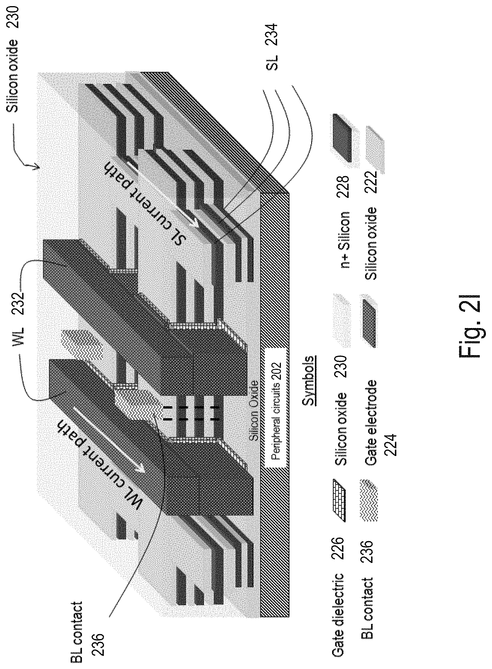
D00013
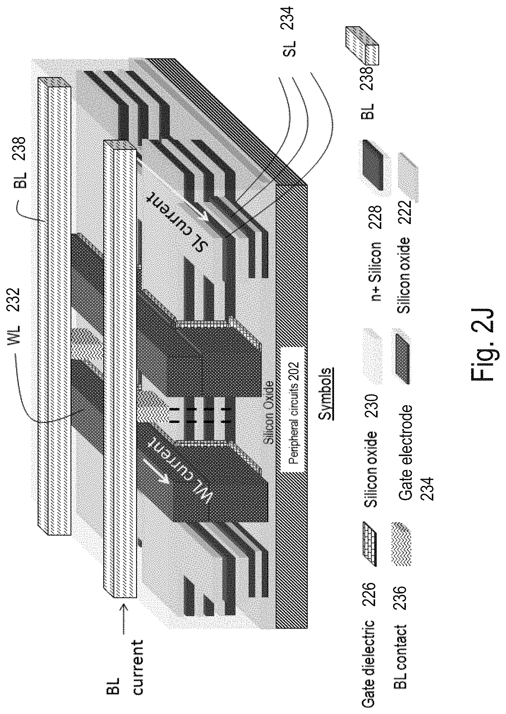
D00014
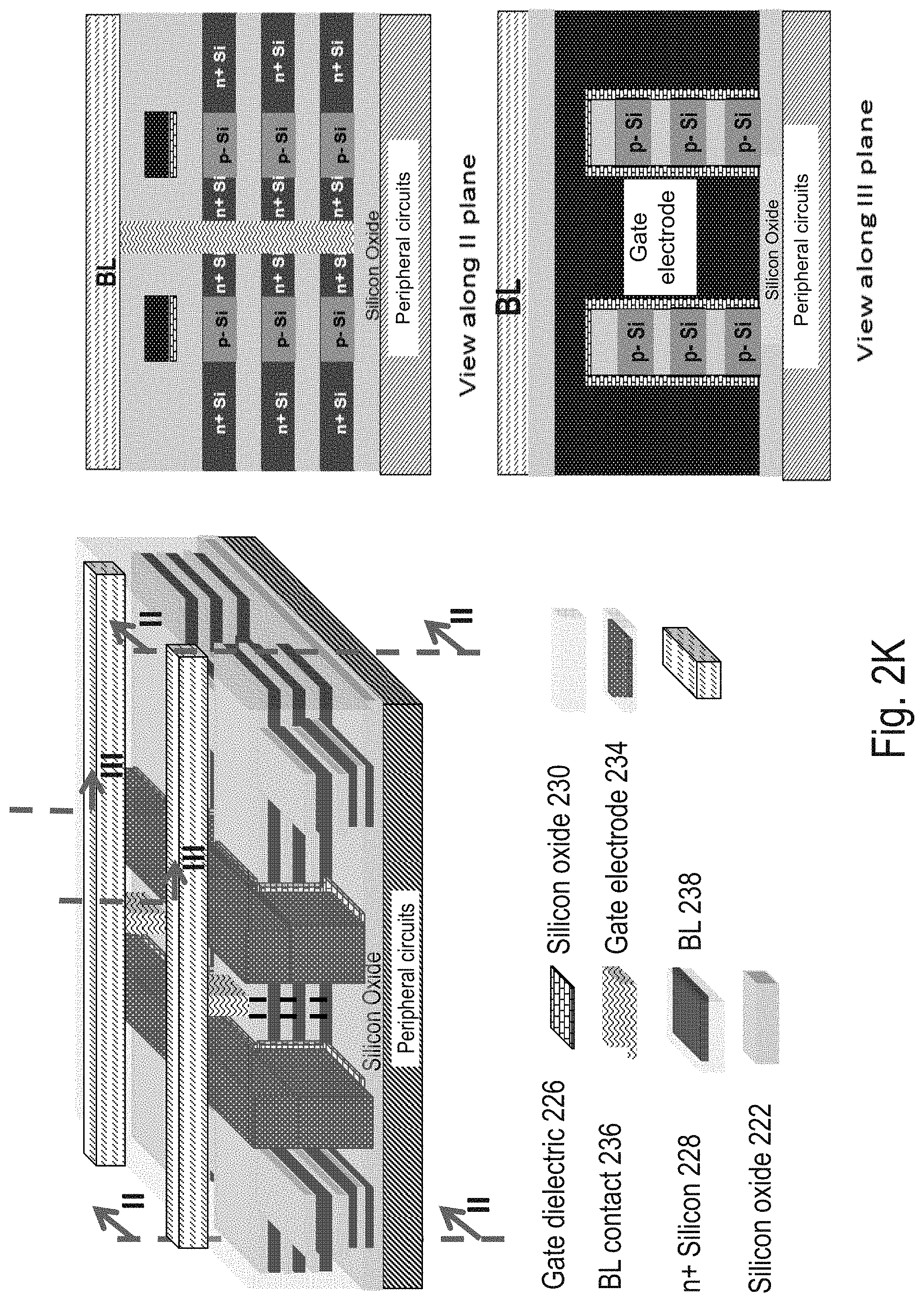
D00015
D00016
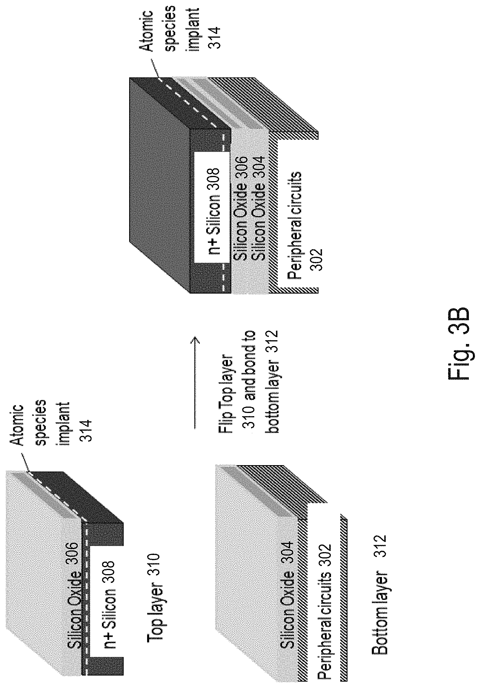
D00017

D00018
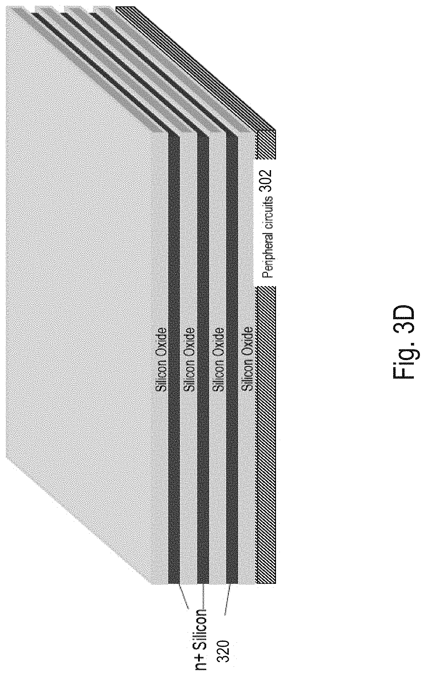
D00019

D00020
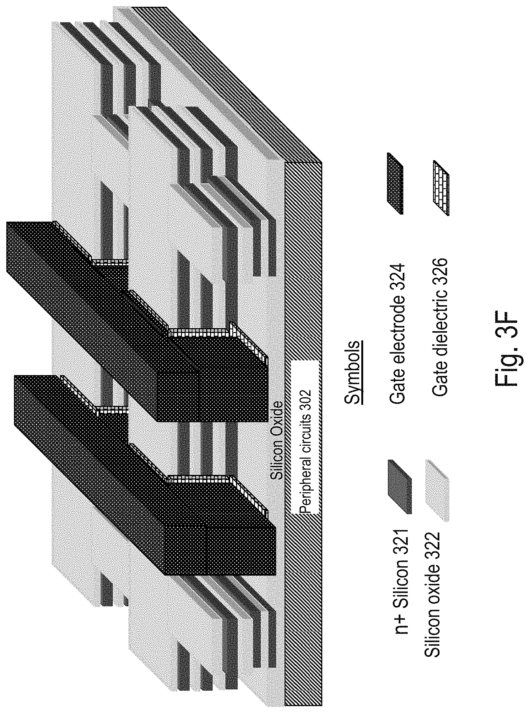
D00021

D00022
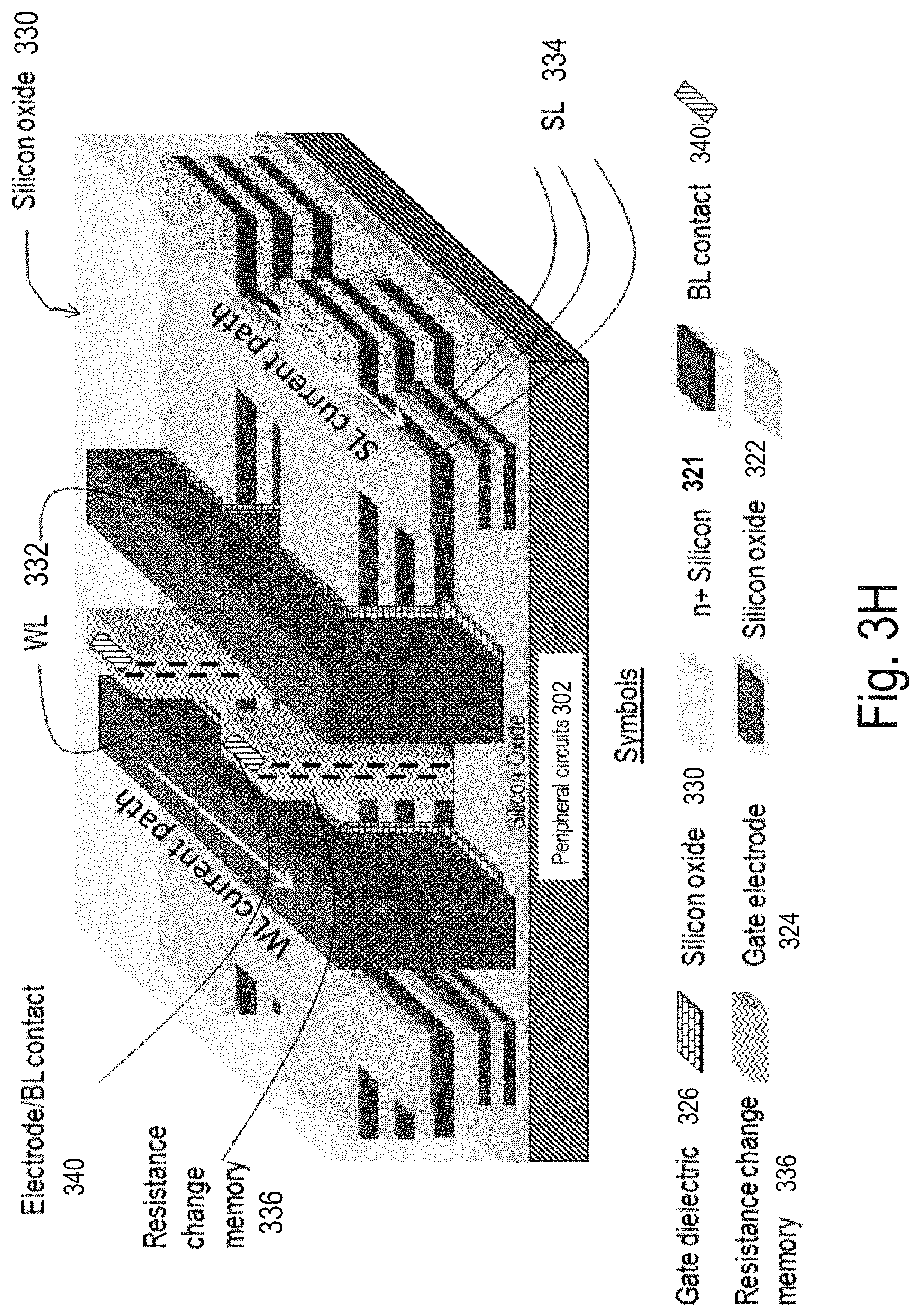
D00023

D00024
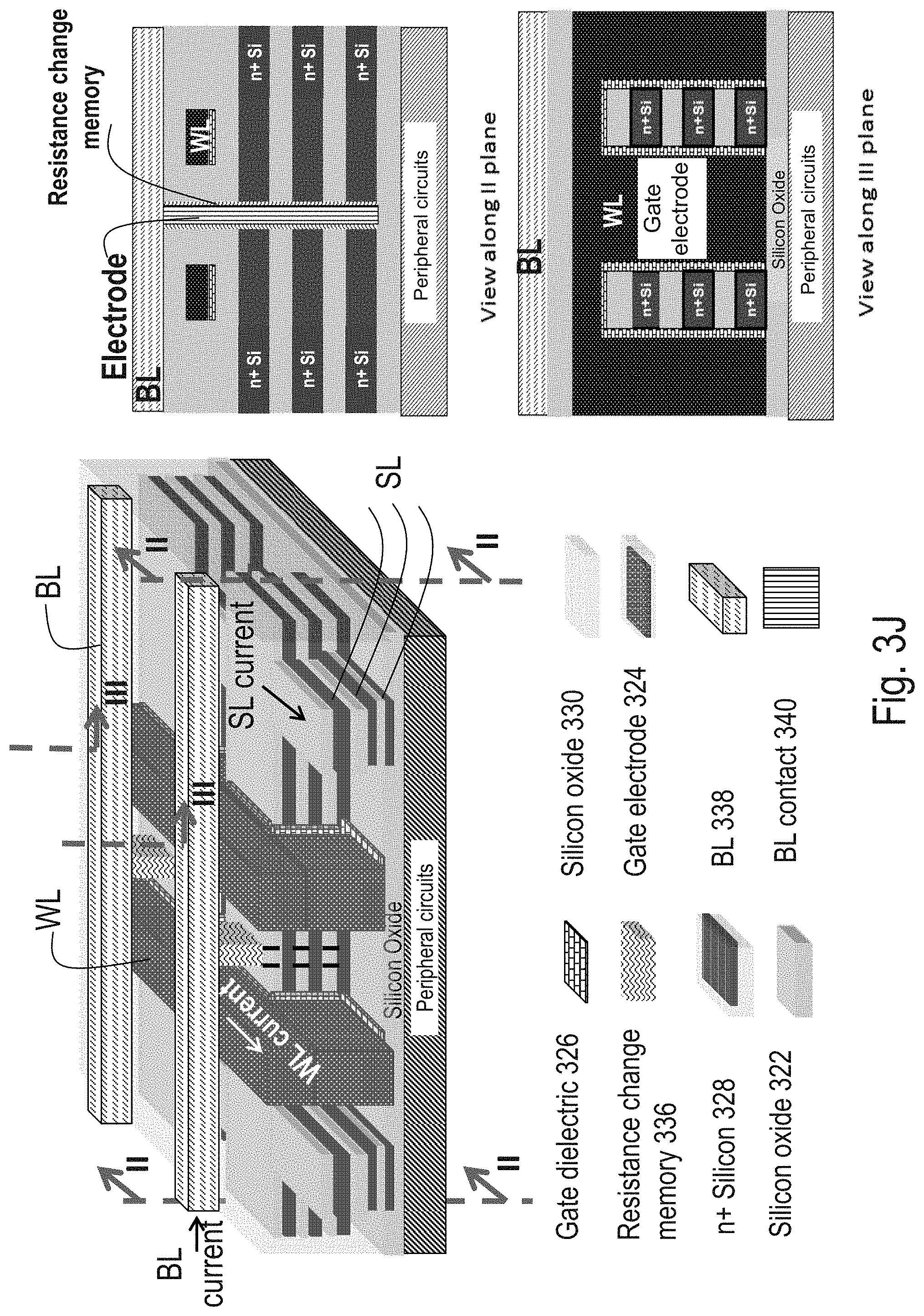
D00025

D00026

D00027

D00028

D00029
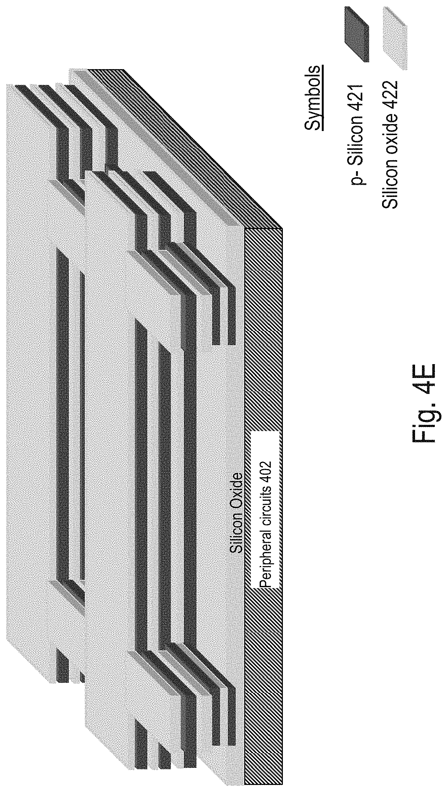
D00030

D00031

D00032
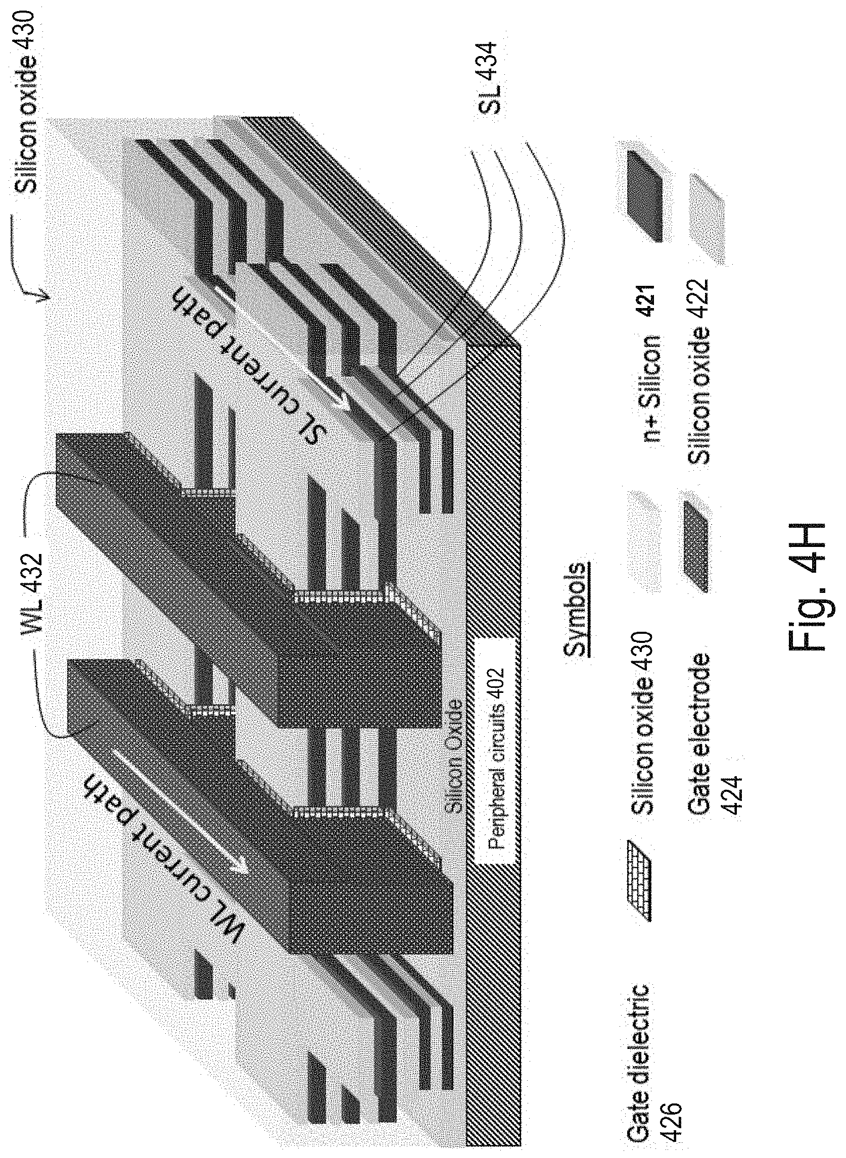
D00033

D00034
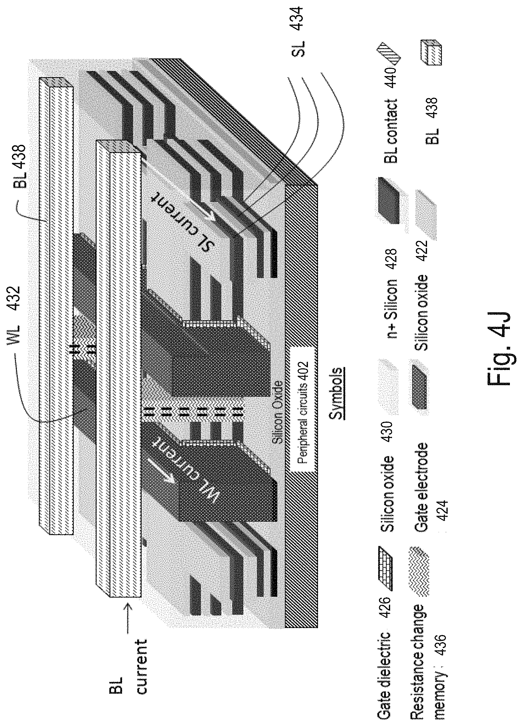
D00035

D00036
D00037
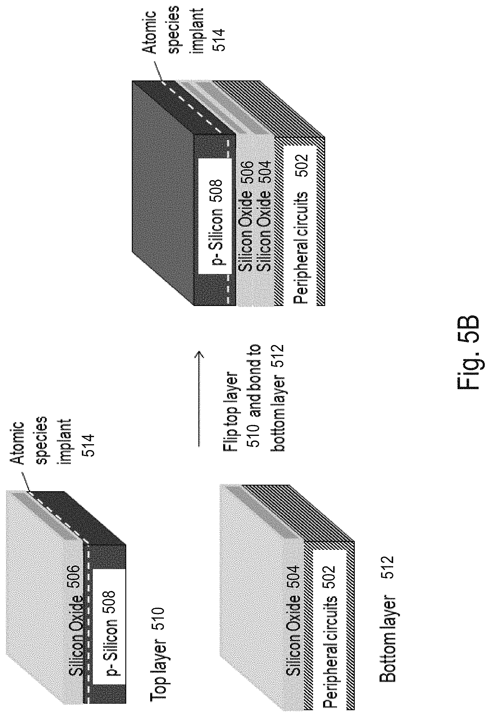
D00038
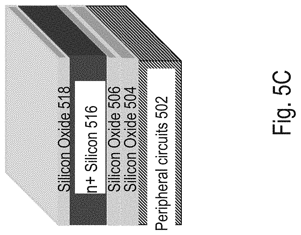
D00039

D00040
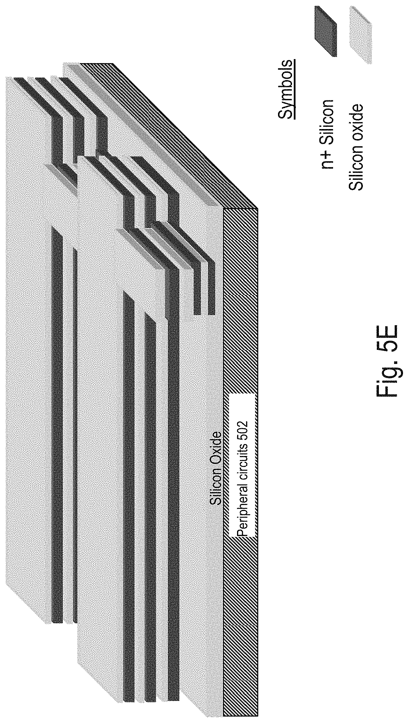
D00041

D00042

D00043

D00044

D00045

D00046

D00047
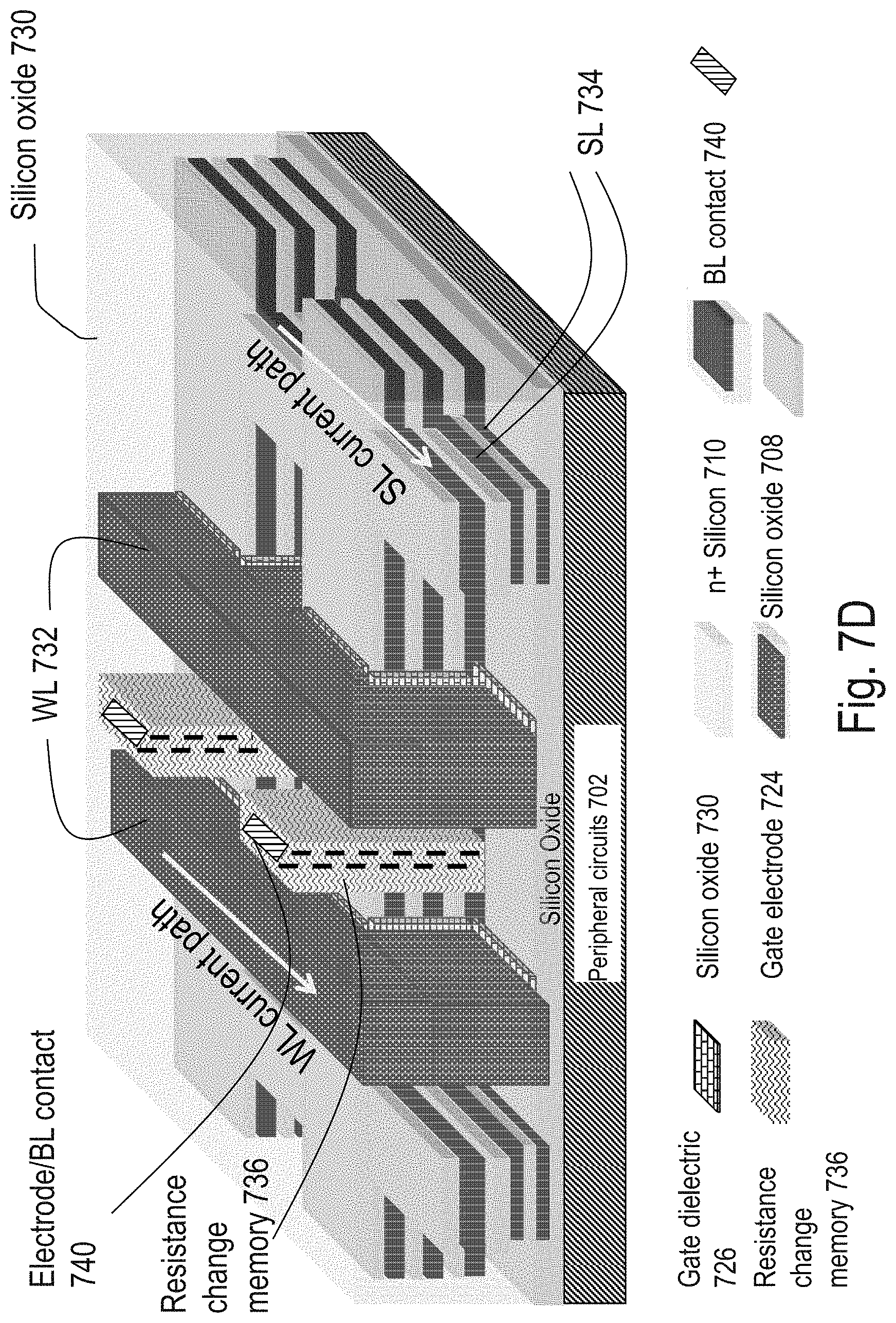
D00048
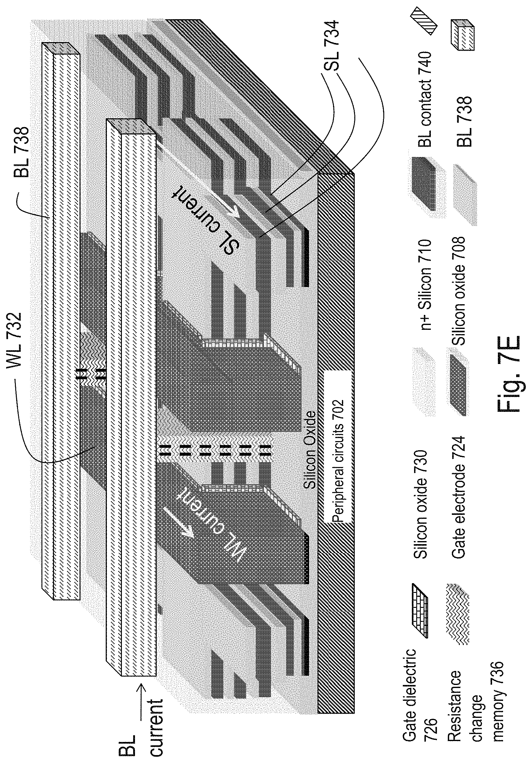
D00049
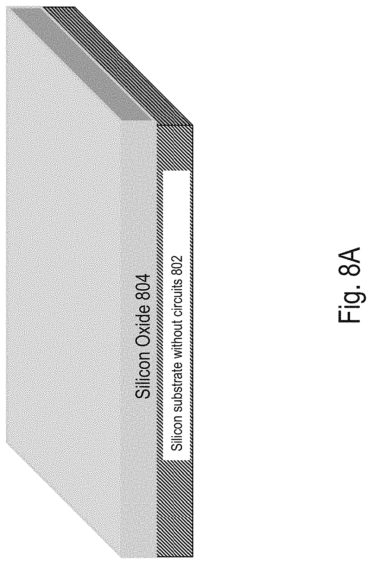
D00050
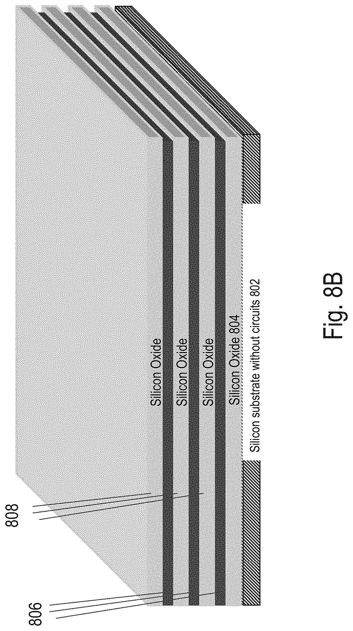
D00051
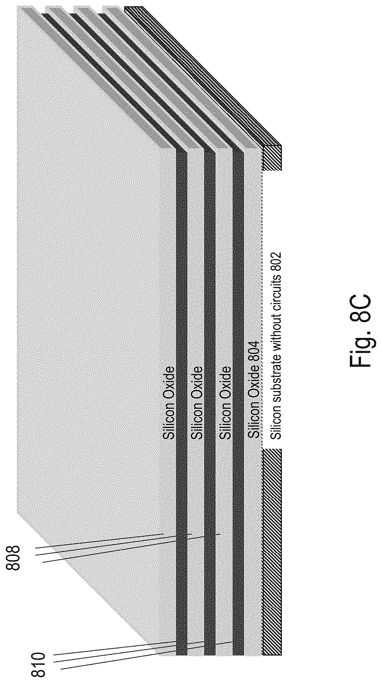
D00052
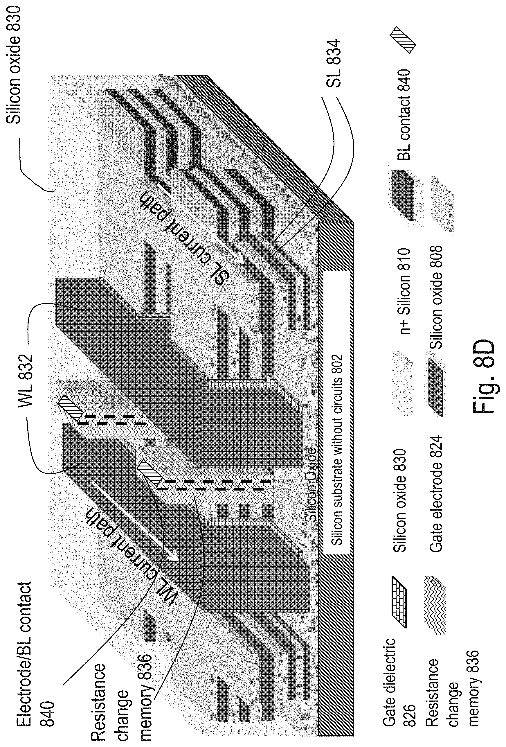
D00053
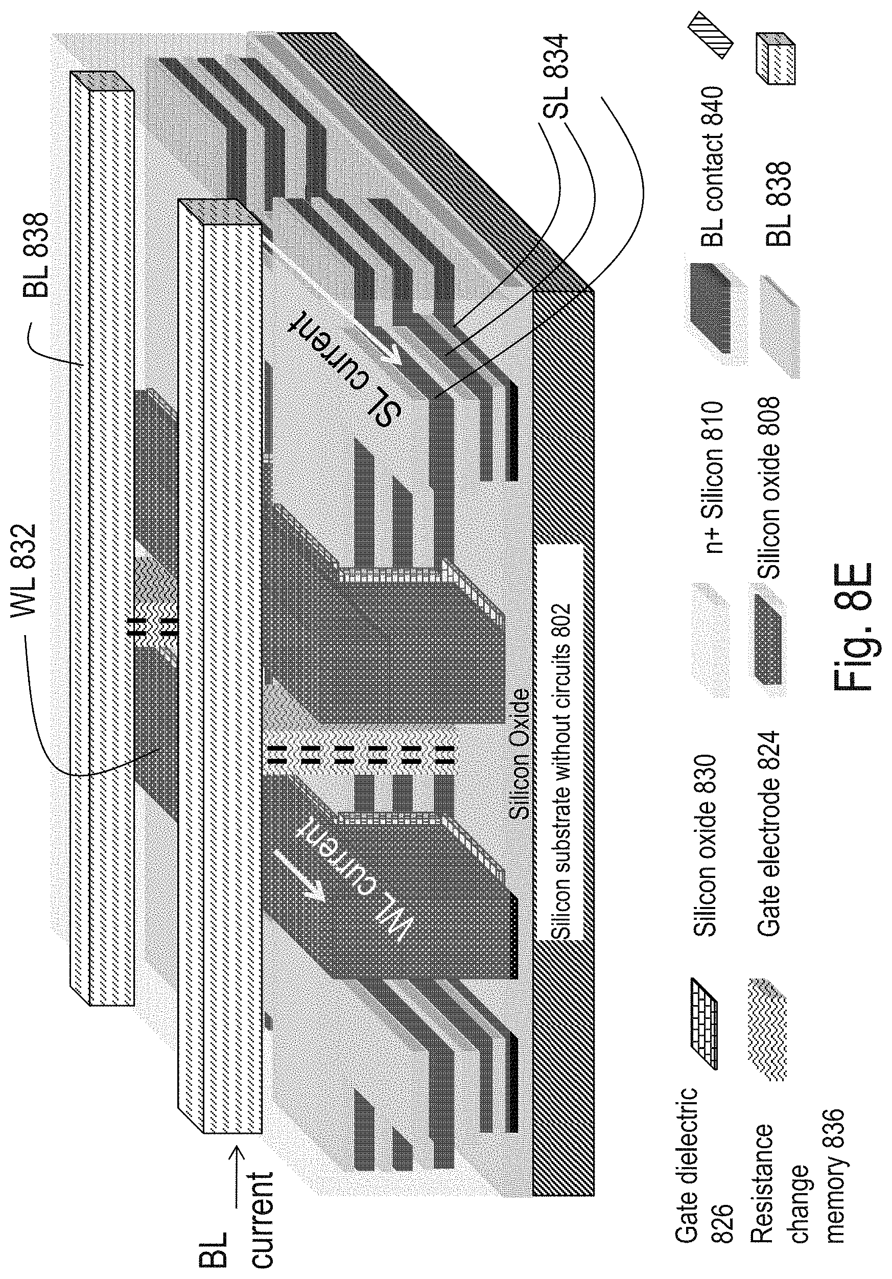
D00054
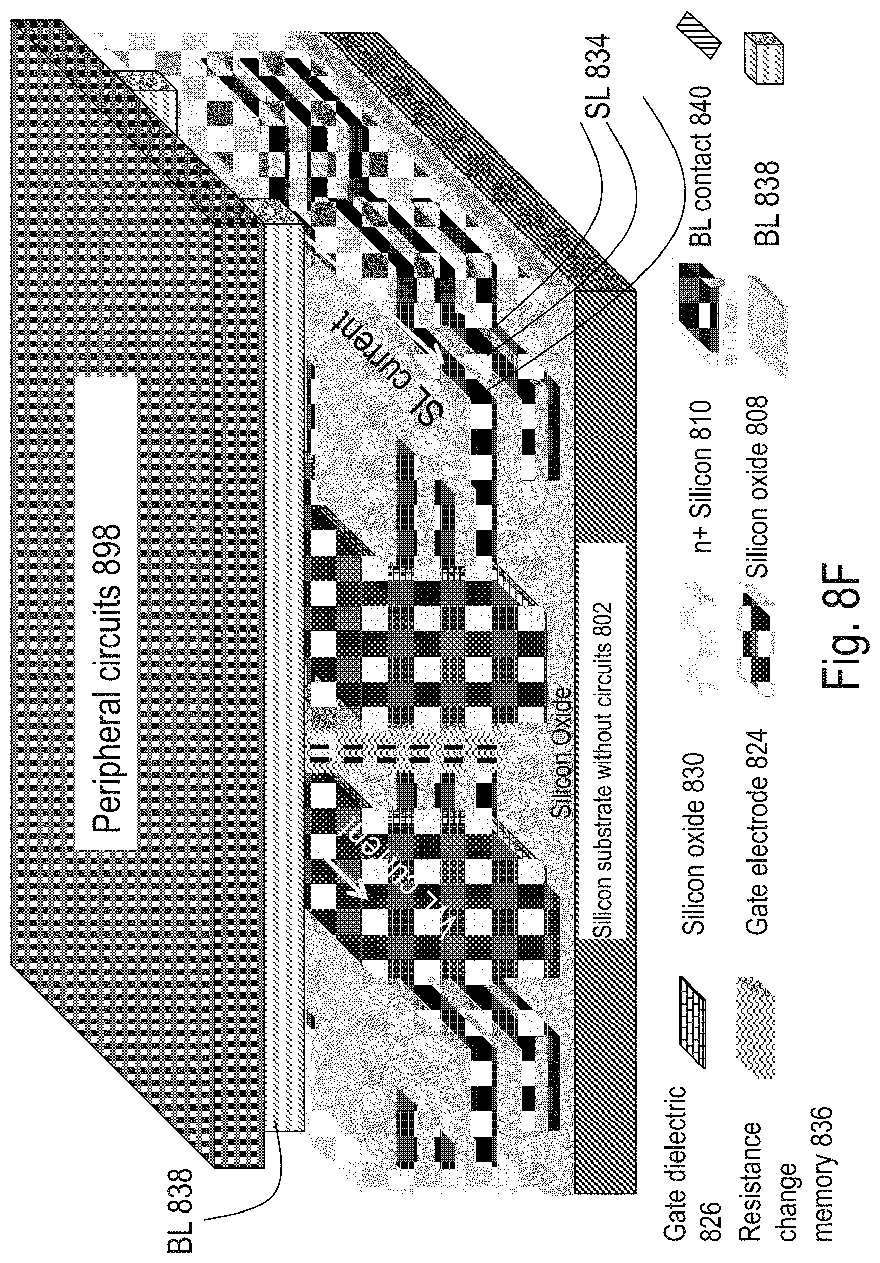
D00055
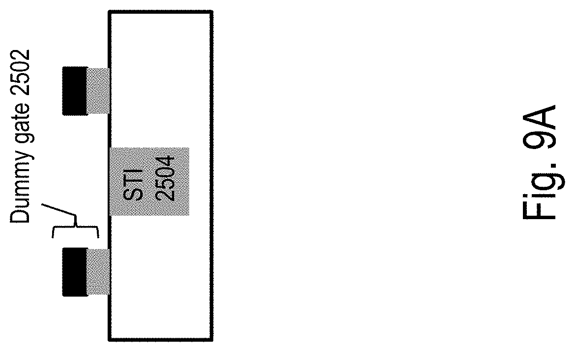
D00056

D00057

D00058
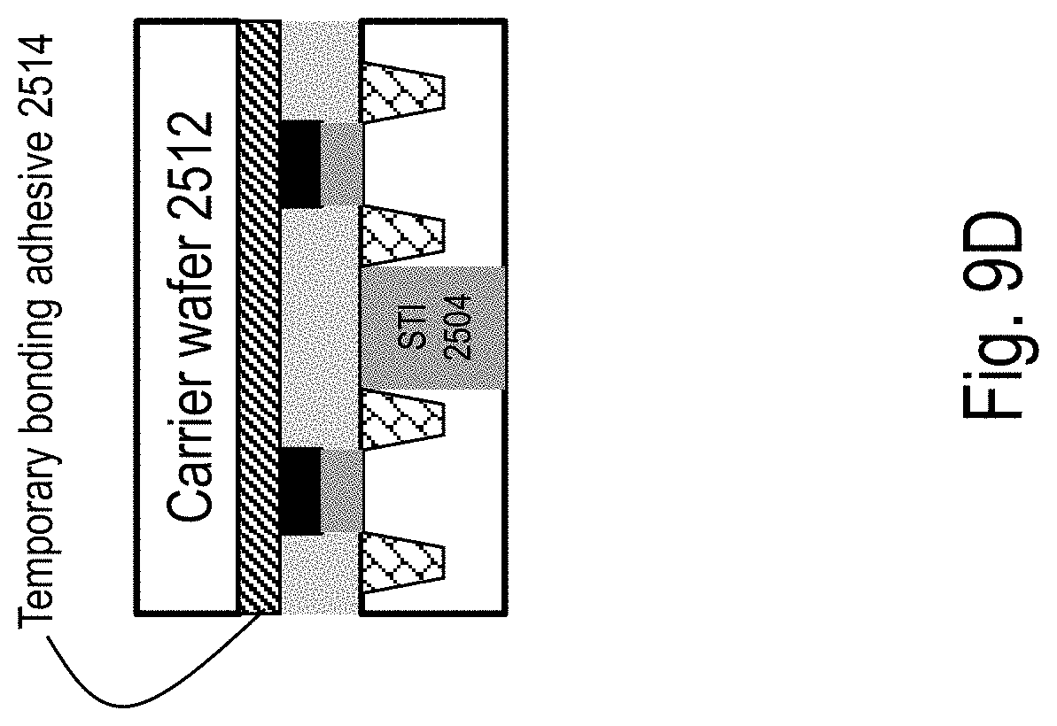
D00059
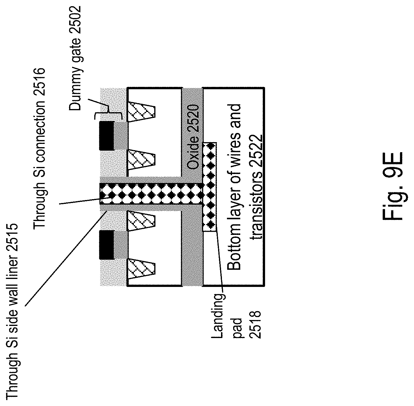
D00060
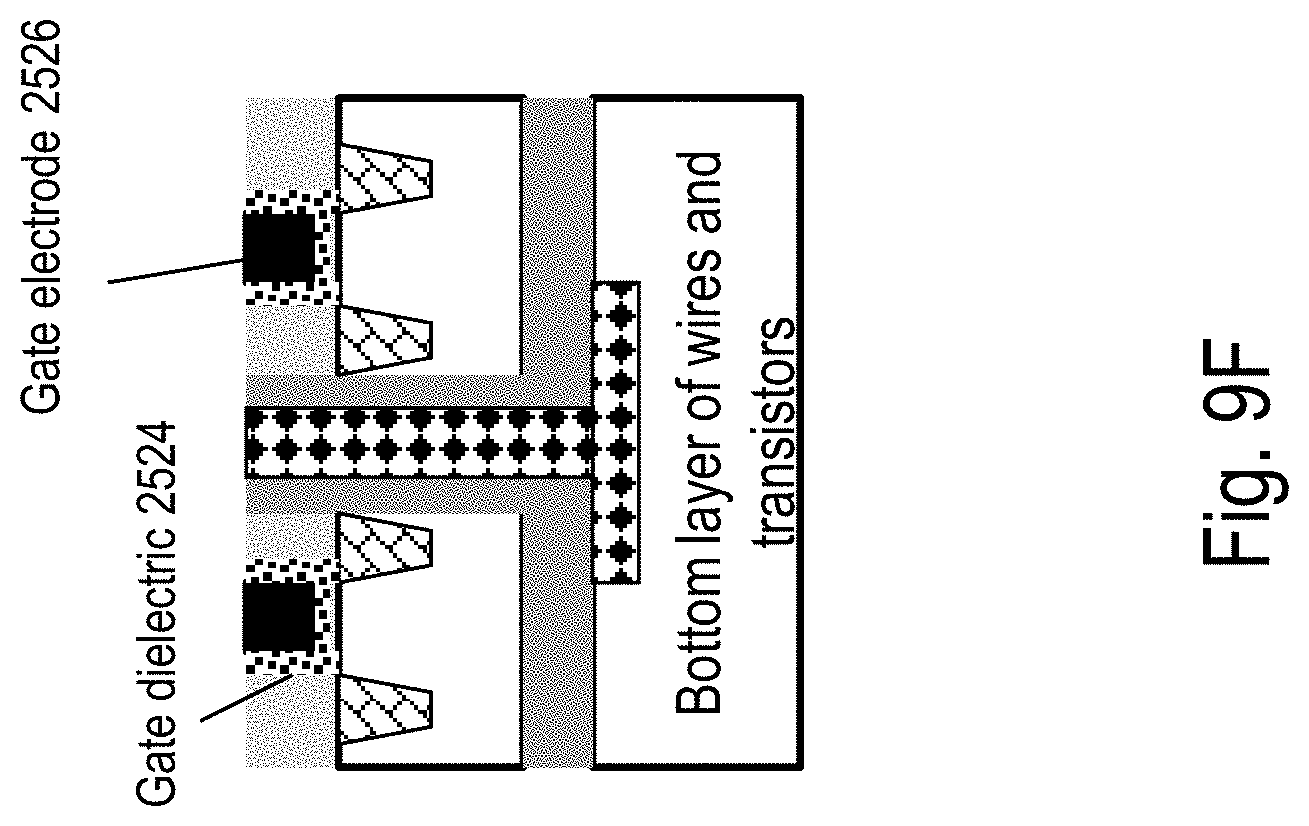
D00061
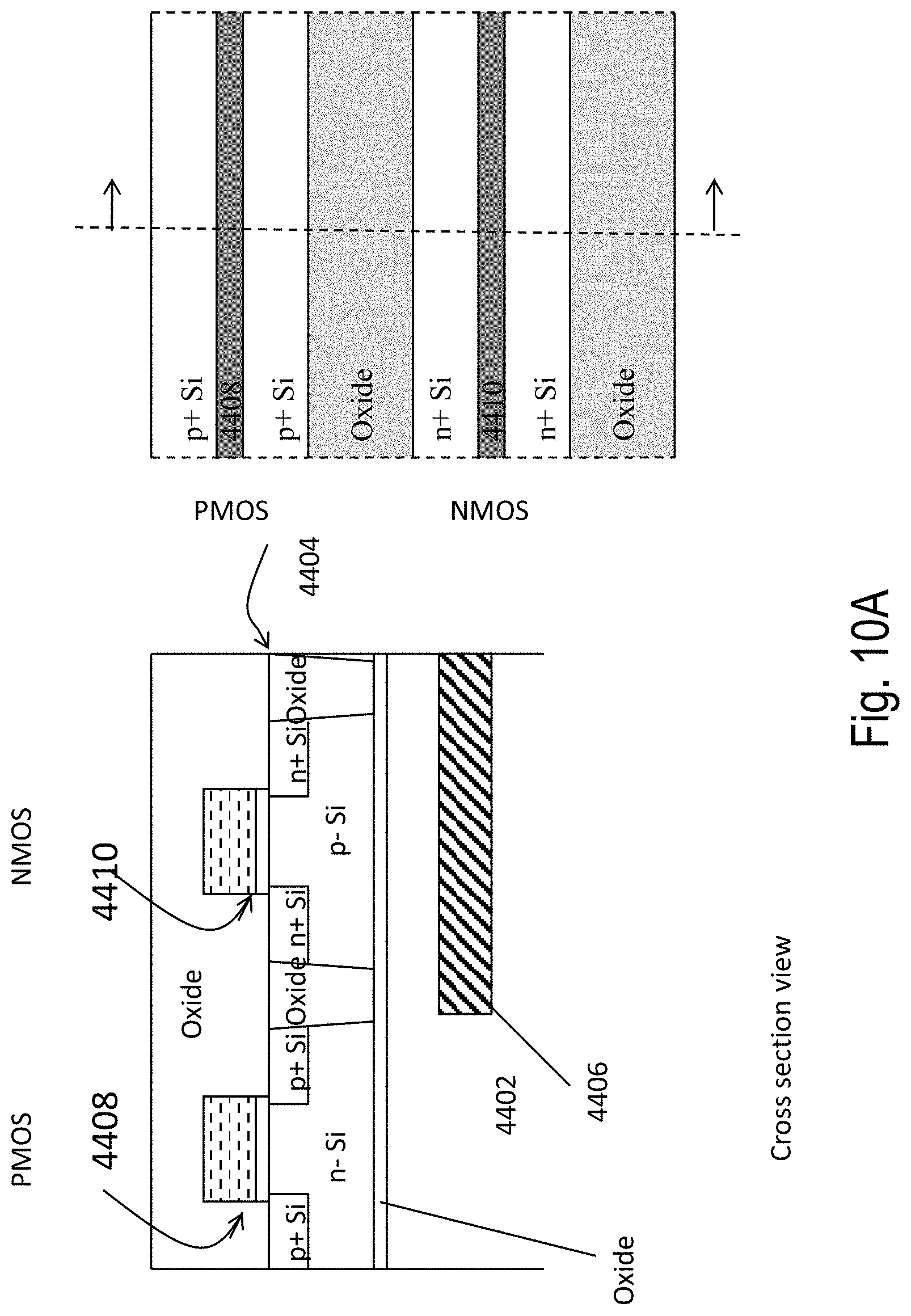
D00062
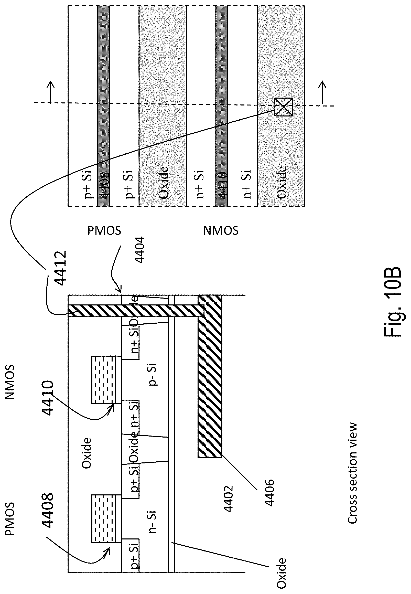
D00063
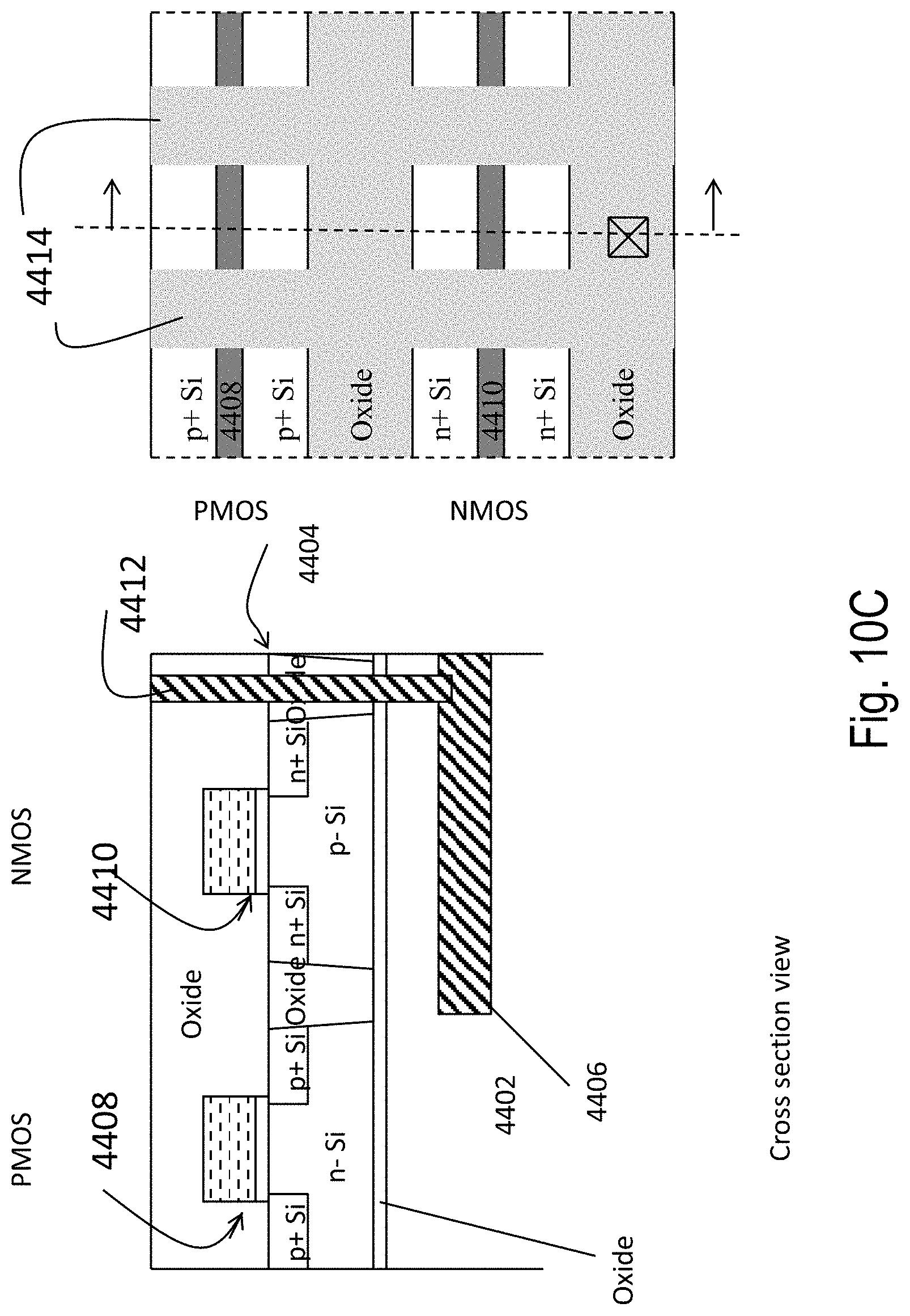
D00064

D00065
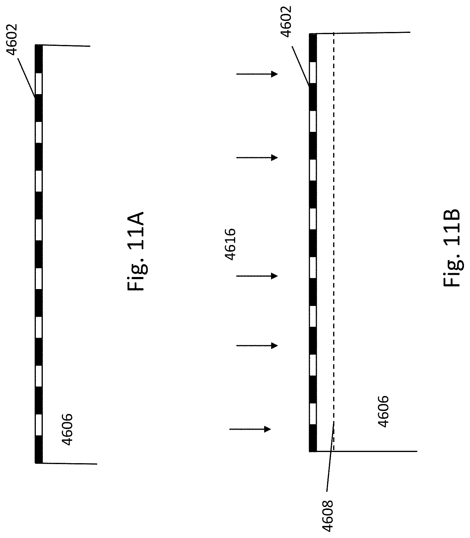
D00066

D00067

D00068
D00069

D00070
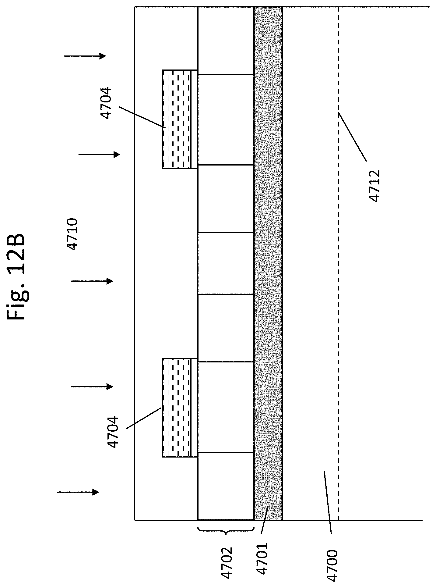
D00071
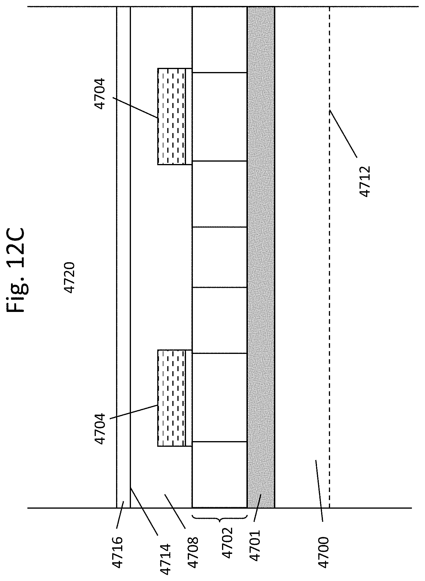
D00072
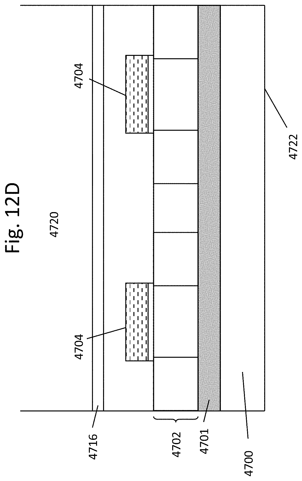
D00073
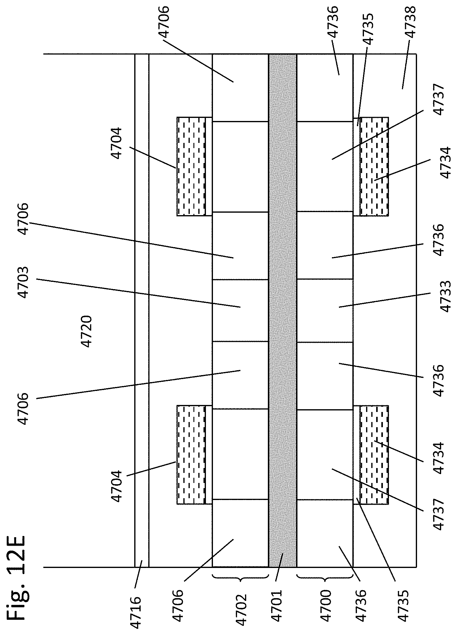
D00074
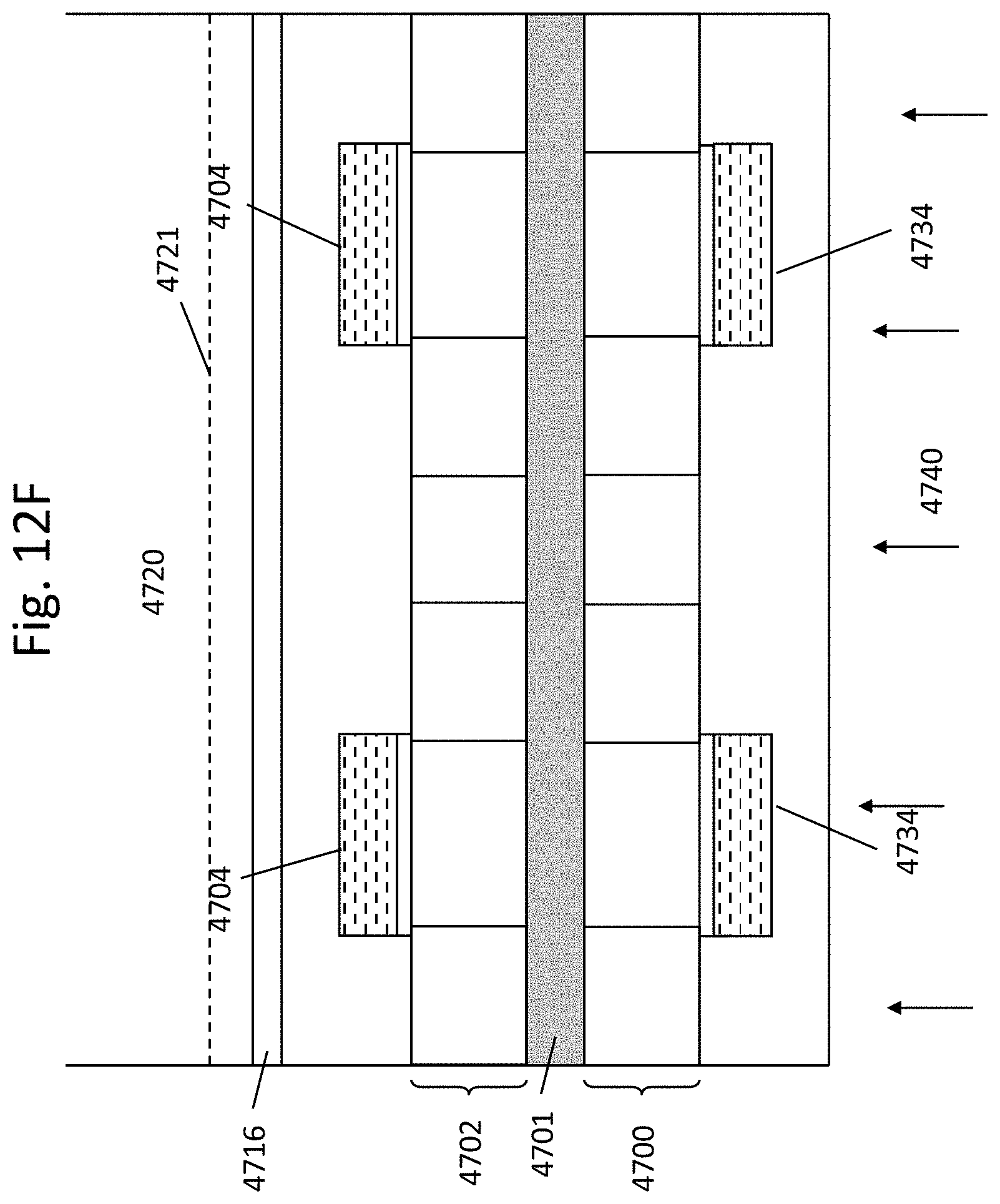
D00075
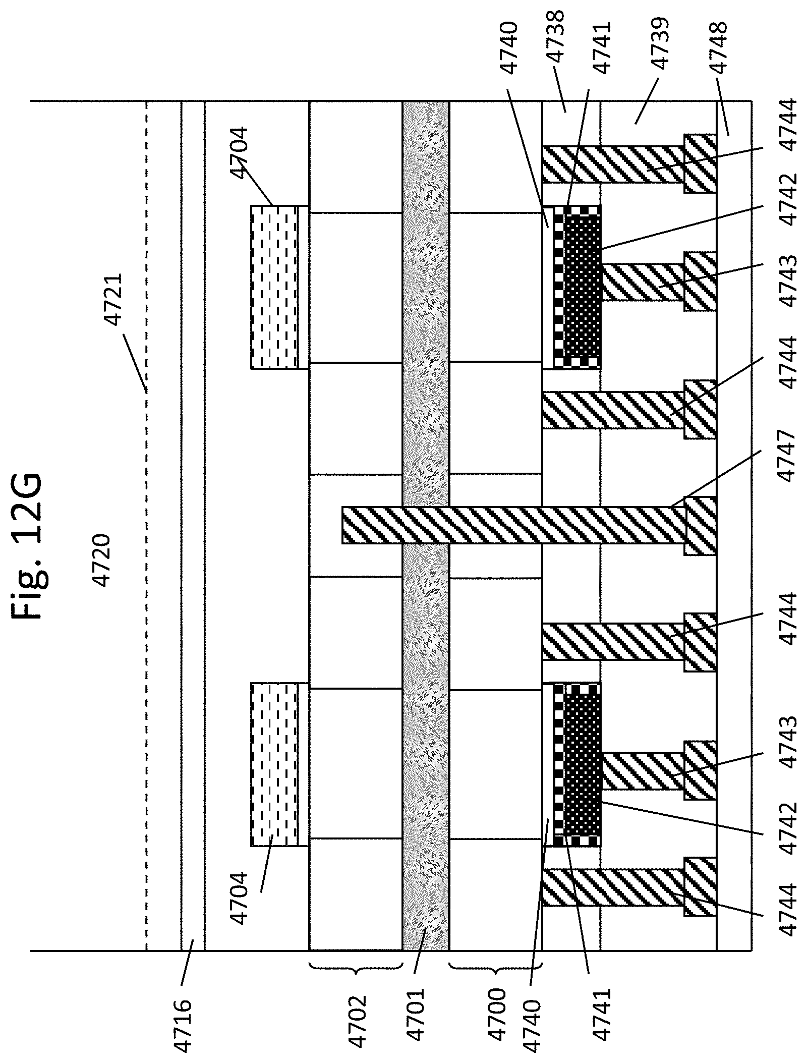
D00076

D00077

D00078

D00079
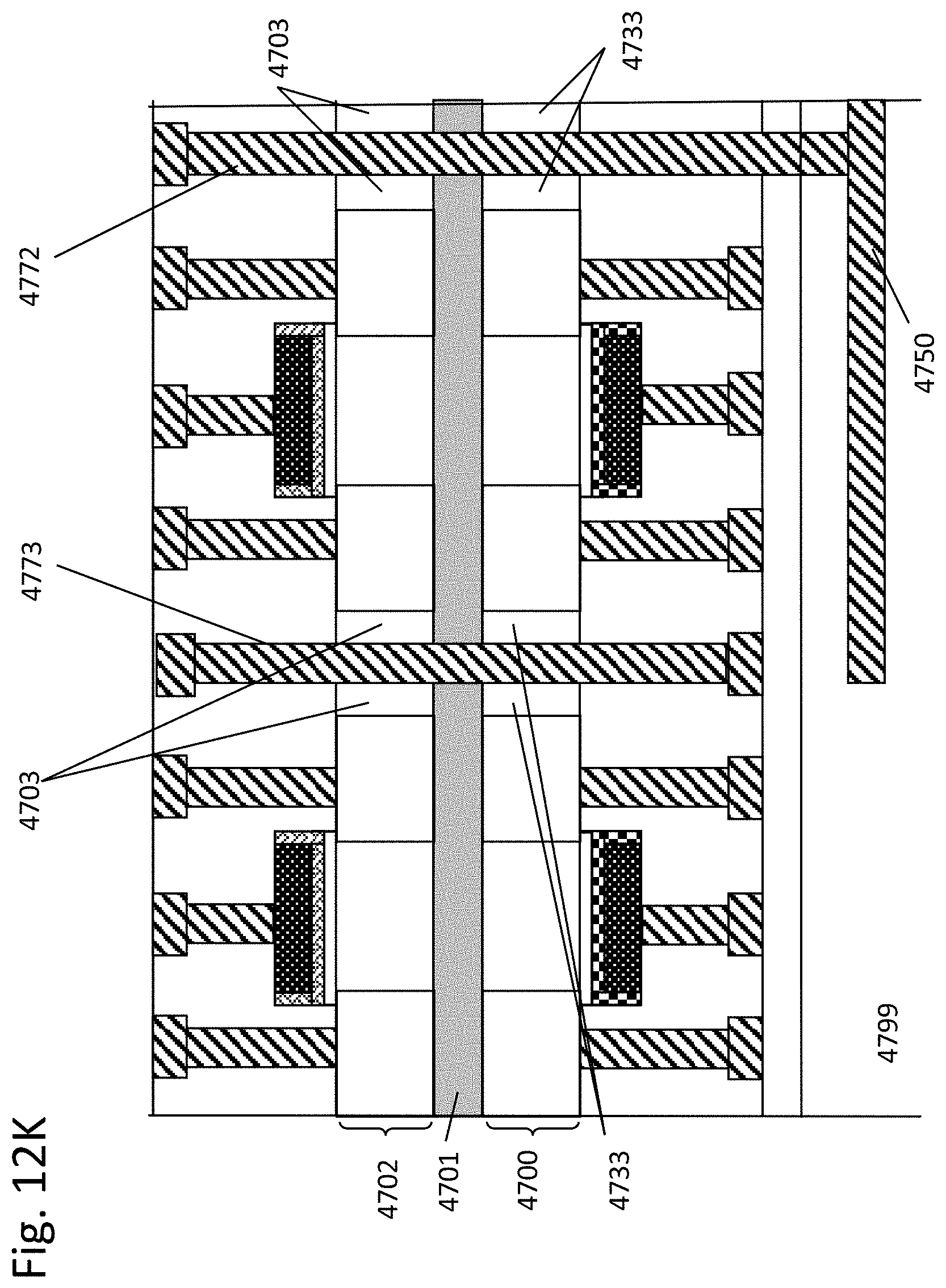
D00080
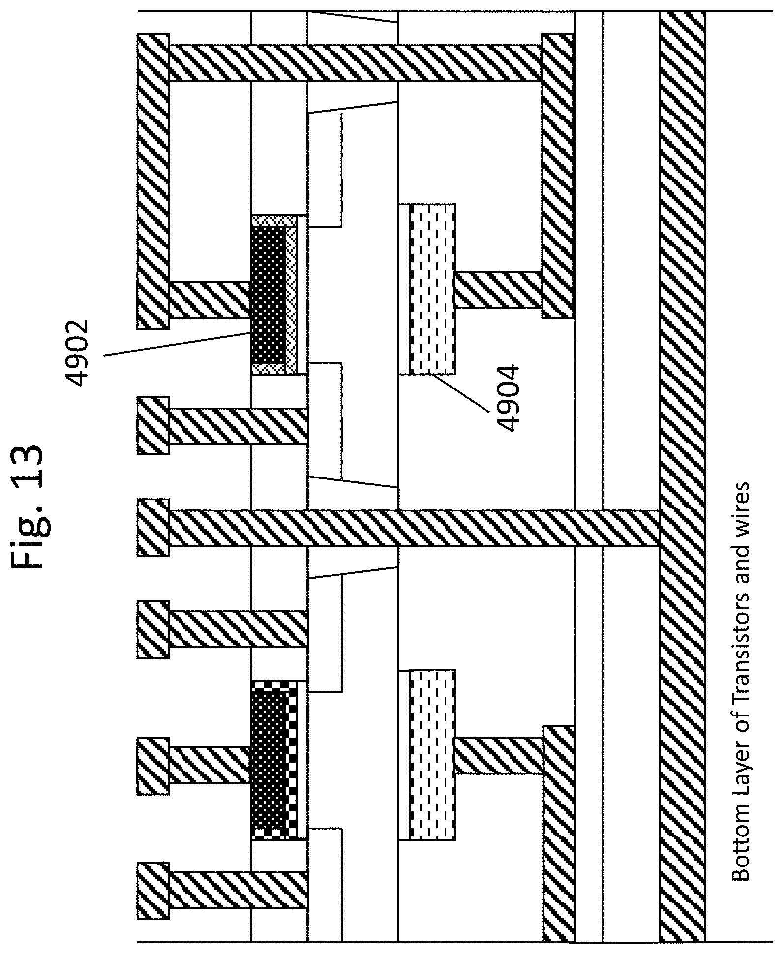
XML
uspto.report is an independent third-party trademark research tool that is not affiliated, endorsed, or sponsored by the United States Patent and Trademark Office (USPTO) or any other governmental organization. The information provided by uspto.report is based on publicly available data at the time of writing and is intended for informational purposes only.
While we strive to provide accurate and up-to-date information, we do not guarantee the accuracy, completeness, reliability, or suitability of the information displayed on this site. The use of this site is at your own risk. Any reliance you place on such information is therefore strictly at your own risk.
All official trademark data, including owner information, should be verified by visiting the official USPTO website at www.uspto.gov. This site is not intended to replace professional legal advice and should not be used as a substitute for consulting with a legal professional who is knowledgeable about trademark law.