Method for manufacturing quantum dot
Kazama , et al. April 27, 2
U.S. patent number 10,988,688 [Application Number 15/666,557] was granted by the patent office on 2021-04-27 for method for manufacturing quantum dot. This patent grant is currently assigned to STANLEY ELECTRIC CO., LTD.. The grantee listed for this patent is STANLEY ELECTRIC CO., LTD.. Invention is credited to Takuya Kazama, Yasuyuki Miyake, Wataru Tamura.


| United States Patent | 10,988,688 |
| Kazama , et al. | April 27, 2021 |
Method for manufacturing quantum dot
Abstract
A quantum dot manufacturing method comprises (a) dispersing, in a solvent, nano-seed particles whose crystal planes are exposed, and (b) growing semiconductor layers on the exposed crystal planes of the nano-seed particles in the solvent.
| Inventors: | Kazama; Takuya (Tokyo, JP), Tamura; Wataru (Yokohama, JP), Miyake; Yasuyuki (Tokyo, JP) | ||||||||||
|---|---|---|---|---|---|---|---|---|---|---|---|
| Applicant: |
|
||||||||||
| Assignee: | STANLEY ELECTRIC CO., LTD.
(Tokyo, JP) |
||||||||||
| Family ID: | 1000005514203 | ||||||||||
| Appl. No.: | 15/666,557 | ||||||||||
| Filed: | August 1, 2017 |
Prior Publication Data
| Document Identifier | Publication Date | |
|---|---|---|
| US 20170355903 A1 | Dec 14, 2017 | |
Related U.S. Patent Documents
| Application Number | Filing Date | Patent Number | Issue Date | ||
|---|---|---|---|---|---|
| PCT/JP2016/000279 | Jan 20, 2016 | ||||
Foreign Application Priority Data
| Feb 2, 2015 [JP] | JP2015-018477 | |||
| Feb 6, 2015 [JP] | JP2015-021936 | |||
| Feb 6, 2015 [JP] | JP2015-021937 | |||
| Current U.S. Class: | 1/1 |
| Current CPC Class: | C30B 29/403 (20130101); C09K 11/0883 (20130101); C09K 11/642 (20130101); C30B 7/14 (20130101); C09K 11/08 (20130101); C09K 11/64 (20130101); C09K 11/62 (20130101); C09K 11/02 (20130101); H01L 33/32 (20130101); B82Y 5/00 (20130101); C09K 11/565 (20130101); Y10S 977/774 (20130101); Y10S 977/824 (20130101); Y10S 977/892 (20130101); Y10S 977/817 (20130101); Y10S 977/95 (20130101); B82Y 40/00 (20130101); H01L 33/502 (20130101); B82Y 20/00 (20130101) |
| Current International Class: | C09K 11/64 (20060101); C09K 11/08 (20060101); C30B 29/40 (20060101); C30B 7/14 (20060101); C09K 11/56 (20060101); H01L 33/32 (20100101); C09K 11/62 (20060101); C09K 11/02 (20060101); B82Y 5/00 (20110101); H01L 33/50 (20100101); B82Y 20/00 (20110101); B82Y 40/00 (20110101) |
References Cited [Referenced By]
U.S. Patent Documents
| 7211143 | May 2007 | Yang et al. |
| 7892452 | February 2011 | Ryowa et al. |
| 9478700 | October 2016 | Daniels et al. |
| 9773942 | September 2017 | Kazama et al. |
| 10032955 | July 2018 | Kazama et al. |
| 2003/0057415 | March 2003 | Komori |
| 2004/0175844 | September 2004 | Yang et al. |
| 2005/0224785 | October 2005 | Komori |
| 2007/0037365 | February 2007 | Ranganath et al. |
| 2010/0163798 | July 2010 | Ryowa et al. |
| 2010/0187497 | July 2010 | Nago et al. |
| 2010/0283005 | November 2010 | Pickett et al. |
| 2011/0263129 | October 2011 | Shin et al. |
| 2013/0270517 | October 2013 | Nozawa et al. |
| 2014/0252316 | September 2014 | Yan |
| 2014/0264172 | September 2014 | Daniels et al. |
| 2015/0194577 | July 2015 | Glarvey et al. |
| 2016/0211409 | July 2016 | Kazama et al. |
| 2017/0009134 | January 2017 | Daniels et al. |
| 2017/0218268 | August 2017 | Pickett et al. |
| 2017/0373223 | December 2017 | Kazama et al. |
| 2018/0047878 | February 2018 | Glarvey et al. |
| 2020/0052169 | February 2020 | Glarvey et al. |
| 105899640 | Aug 2016 | CN | |||
| 3050936 | Aug 2016 | EP | |||
| 2003107546 | Apr 2003 | JP | |||
| 2007050500 | Mar 2007 | JP | |||
| 4318710 | Aug 2009 | JP | |||
| 4502758 | Jul 2010 | JP | |||
| 2011076827 | Apr 2011 | JP | |||
| 2011258994 | Dec 2011 | JP | |||
| 4936338 | May 2012 | JP | |||
| 2012087220 | May 2012 | JP | |||
| 2013239690 | Nov 2013 | JP | |||
Other References
|
Japanese Office Action (and English language translation thereof) dated Dec. 10, 2019 issued in counterpart Japanese Application No. 2016-008999. cited by applicant . International Search Report (ISR) and Written Opinion dated Apr. 12, 2016 issued in International Application No. PCT/JP2016/000279. cited by applicant . Extended European Search Report (EESR) dated Jul. 31, 2018 issued in counterpart European Application No. 16746269.6. cited by applicant . Chinese Office Action (and English translation thereof) dated Jan. 3, 2020, issued in counterpart Chinese Application No. 201680008020.0. cited by applicant. |
Primary Examiner: Johnson; Edward M
Attorney, Agent or Firm: Holtz, Holtz & Volek PC
Claims
What are claimed are:
1. A quantum dot manufacturing method comprising: (a) dispersing, in a solvent, nano-seed particles whose crystal planes are exposed; and (b) growing flat-plate-shaped first nitride semiconductor layers epitaxially on the exposed crystal planes of the nano-seed particles in the solvent, the first nitride semiconductor layers being made of In.sub.x(Al.sub.mGa.sub.n).sub.1-xN (0.15.ltoreq.x.ltoreq.1.0, m+n=1.0).
2. The quantum dot manufacturing method according to claim 1, wherein the step (a) comprises: (a1) preparing base particles made of group II-VI semiconductor material containing Zn or Mg as group II element; and (a2) forming the nano-seed particles by etching the base particles in liquid phase.
3. The quantum dot manufacturing method according to claim 2, wherein, in the substep (a2), the base particles are etched by a selective photoetching process.
4. The quantum dot manufacturing method according to claim 3, wherein the nano-seed particles are formed by etching the base particles with an etching solution containing nitric acid, C-planes of the nano-seed particles being exposed.
5. The quantum dot manufacturing method according to claim 3, wherein the nano-seed particles are formed by etching the base particles with an etching solution containing aqua regia, M-planes of the nano-seed particles being exposed.
6. The quantum dot manufacturing method according to claim 2, wherein, in the substep (a2), each crystal plane of the nano-seed particles has a maximum width in an in-plane direction of 20 nm or less.
7. The quantum dot manufacturing method according to claim 2, wherein, in the substep (a1), the base particles contain ZnOS.
8. The quantum dot manufacturing method according to claim 1, wherein, in the step (b), second nitride semiconductor layers made of In.sub.y(Al.sub.pGa.sub.q).sub.1-yN (0.15.ltoreq.y.ltoreq.1.0, p+q=1.0) and having different composition from the first nitride semiconductor layers are epitaxially grown on the first nitride semiconductor layers.
9. The quantum dot manufacturing method according to claim 8, wherein, in the step (b), third nitride semiconductor layers having the same composition as the first nitride semiconductor layers are epitaxially grown on the second nitride semiconductor layers.
10. The quantum dot manufacturing method according to claim 1, wherein, in the step (b), first semiconductor layers, seed layers having the same composition as the nano-seed particles, and second semiconductor layers are sequentially epitaxially grown on the crystal planes of the nano-seed particles, wherein the method further comprises (c) removing the nano-seed particles and the seed layers to separate the first and second semiconductor layers from each other, and wherein the first semiconductor layers include the first nitride semiconductor layers made of In.sub.x(Al.sub.mGa.sub.n).sub.1-xN (0.15.ltoreq.x.ltoreq.1.0, m+n=1.0).
11. The quantum dot manufacturing method according to claim 10, further comprising (d) covering each of the first and second semiconductor layers, which are separated from each other, with third semiconductor layers.
12. The quantum dot manufacturing method according to claim 11, wherein each of the second semiconductor layers includes a layer having a composition corresponding to the first nitride semiconductor layers made of In.sub.x(Al.sub.mGa.sub.n).sub.1-xN (0.15.ltoreq.x.ltoreq.1.0, m+n=1.0).
13. The quantum dot manufacturing method according to claim 12, wherein each of the first and second semiconductor layers further includes a second nitride semiconductor layer made of In.sub.y(Al.sub.pGa.sub.q).sub.1-yN (0.15.ltoreq.y.ltoreq.1.0, p+q=1.0) and having different composition from the first nitride semiconductor layer.
14. The quantum dot manufacturing method according to claim 13, wherein the third semiconductor layer has the same composition as the first nitride semiconductor layers.
15. The quantum dot manufacturing method according to claim 1, wherein in the step (b), first semiconductor layers having plate shapes with thicknesses such that a quantum confinement effect occurs are epitaxially grown on the crystal planes of the nano-seed particles, wherein the method further comprises: (c) removing the nano-seed particles after growing the first semiconductor layer; and (d) sequentially epitaxially growing second and third semiconductor layers, having plate shapes with thicknesses such that a quantum confinement effect occurs, on main surfaces of the first semiconductor layers, and wherein the first semiconductor layers include the first nitride semiconductor layers made of In.sub.x(Al.sub.mGa.sub.n).sub.1-xN (0.15.ltoreq.x.ltoreq.1.0, m+n=1.0).
Description
FIELD OF THE INVENTION
The present invention relates to a quantum dot manufacturing method and a quantum dot.
BACKGROUND
A substance made as small (fine or thin) as about several nanometers up to less than 20 nanometers in size begins to exhibit physical properties different from those in its bulk state. This phenomenon or effect is called a (three to one dimensional) carrier confinement effect or a quantum size effect, and a substance that displays such an effect is called a quantum dot (quantum wire or quantum well) or a semiconductor nanoparticle, for example. The bandgap (optical absorption wavelength or emission wavelength) of a quantum dot can be adjusted by changing the size (overall size) of the quantum dot.
One usage of a quantum dot containing a semiconductor material is a fluorescent material. A quantum dot containing a semiconductor material can emit florescence of a particular wavelength when irradiated with high-energy light or particle radiation. An area light source can be obtained by evenly distributing quantum dots and causing the quantum dots to emit light.
Quantum dots having a core-shell structure in which a core (nucleus) portion is covered with a shell layer are available (for example, Japanese Laid-open Patent Publication Nos. 2011-076827 and 2012-087220, and Japanese Patent Nos. 4936338 and 4318710). These quantum dots can be manufactured by, for example, a liquid phase growth method (for example, Japanese Patent Nos. 4936338, 4318710 and 4502758).
SUMMARY
A main object of the present invention is to obtain a quantum dot having a novel structure. Another object of the present invention is to obtain a quantum dot that has high reliability and excellent efficiency. Yet another object of the present invention is to efficiently manufacture quantum dots.
According to an aspect of this invention, there is provided a quantum dot manufacturing method comprising (a) dispersing, in a solvent, nano-seed particles whose crystal planes are exposed, and (b) growing semiconductor layers on the exposed crystal planes of the nano-seed particles in the solvent.
A quantum dot having a novel structure (flat multilayer structure) and a quantum dot having high reliability and excellent efficiency can be obtained through the present invention. Moreover, quantum dots can be manufactured more efficiently.
BRIEF DESCRIPTION OF THE DRAWINGS
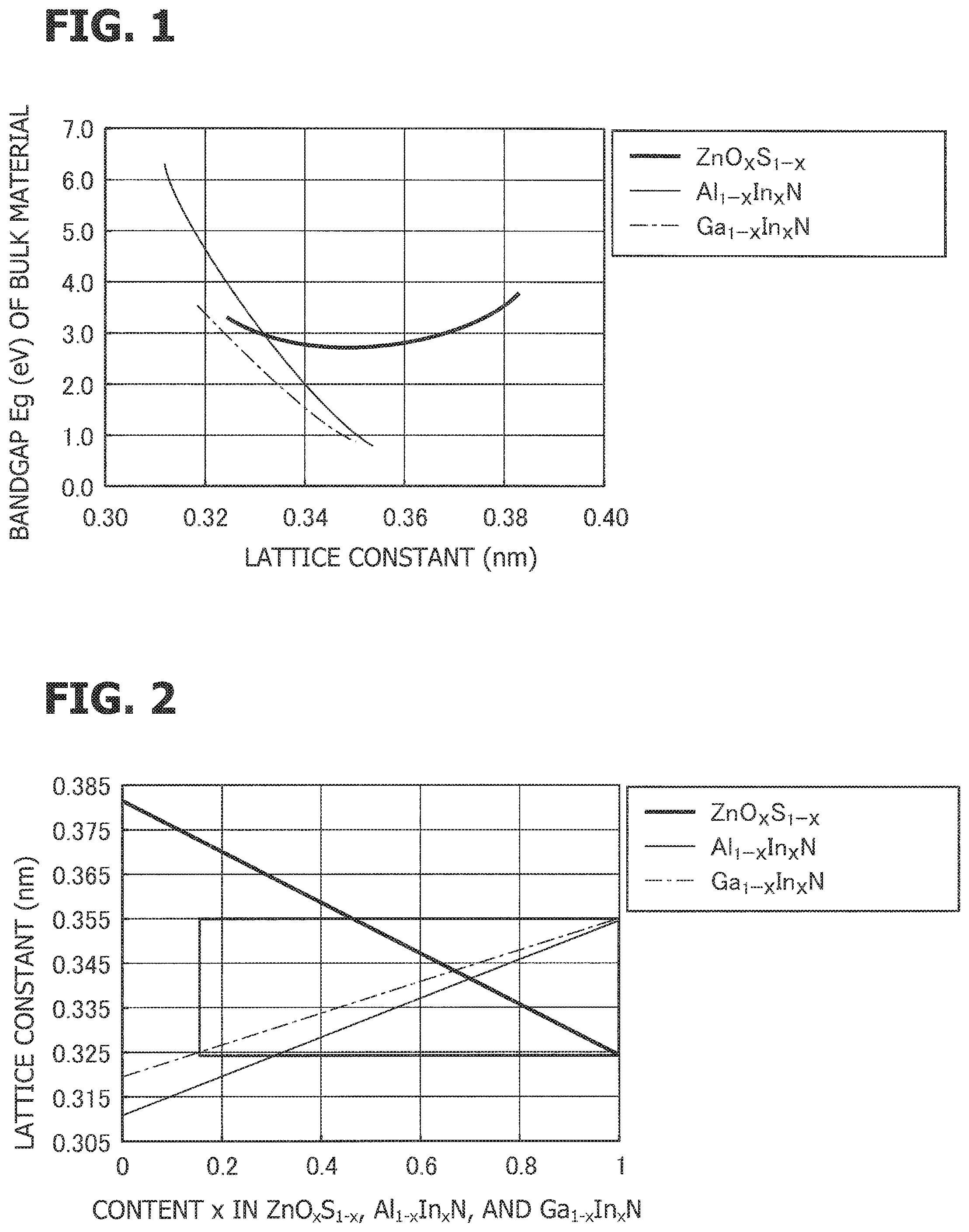
FIG. 1 is a graph showing the relationships between lattice constants of a ZnOS mixed crystal system, a GaInN mixed crystal system, and an AlInN mixed crystal system, and the energy gap.
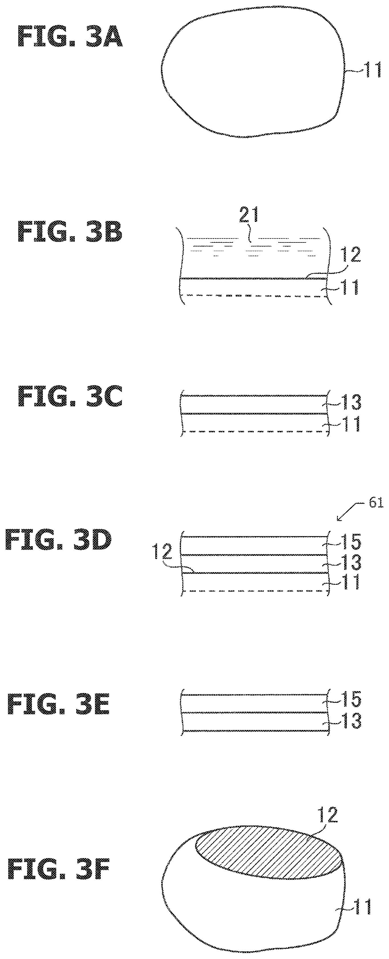
FIG. 2 is a graph showing changes in lattice constants of a ZnO.sub.xS.sub.1-x mixed crystal system, a Ga.sub.1-xIn.sub.xN mixed crystal system, and an Al.sub.1-xIn.sub.xN mixed crystal system relative to the content x.
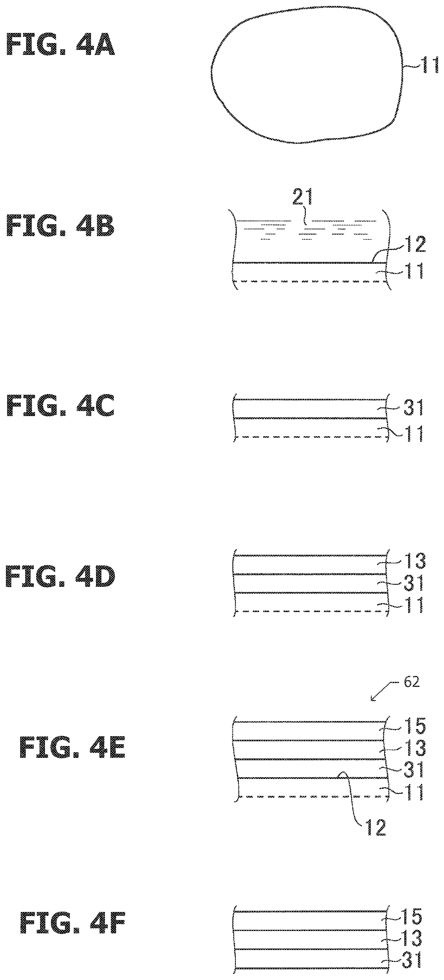
FIGS. 3A to 3D are schematic cross-sectional views of a quantum dot manufacturing process according to a first embodiment, and FIGS. 3E and 3F are respectively a cross-sectional view and a perspective view schematically illustrating a modification example.
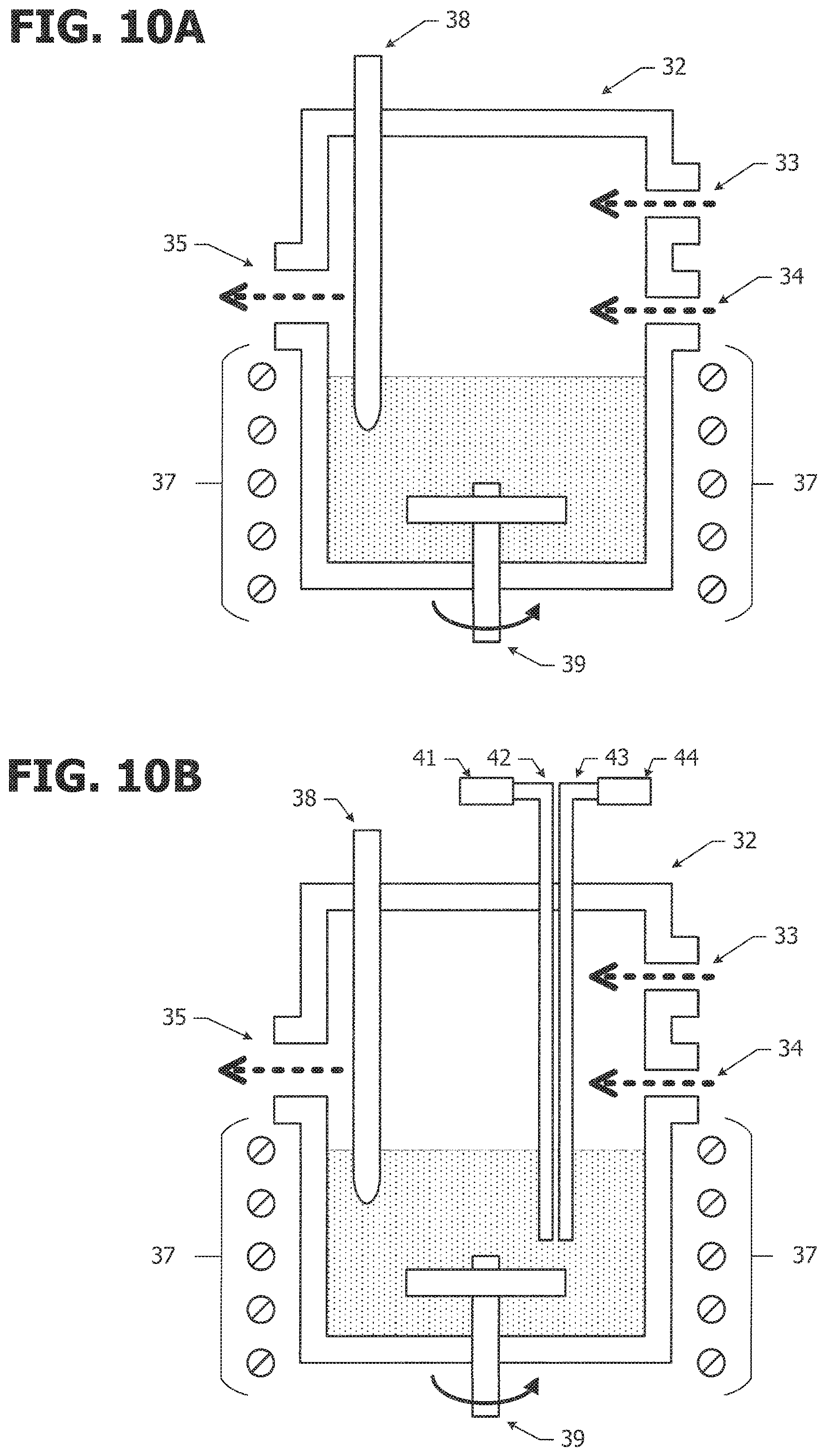
FIGS. 4A to 4E are schematic cross-sectional views of a quantum dot manufacturing process according to a second embodiment, and FIG. 4F is a schematic cross-sectional view of a modification example.
FIGS. 5A to 5E are schematic cross-sectional views of a quantum dot manufacturing process according to a third embodiment.
FIGS. 6A to 6E are schematic cross-sectional views of a quantum dot manufacturing process according to a fourth embodiment.
FIGS. 7A to 7D are schematic cross-sectional views of a quantum dot manufacturing process according to a fifth embodiment, FIG. 7E is a schematic cross-sectional view of a quantum dot according to a reference example, and FIG. 7F is a schematic cross-sectional view of a quantum dot according to a sixth embodiment.
FIG. 8 is a schematic side view of an example of a reactor.
FIG. 9 is a schematic side view of an example of an etching device.
FIGS. 10A and 10B are schematic side views of examples of pressure reactors.
DESCRIPTION OF THE PREFERRED EMBODIMENTS
First Embodiment
Quantum dots in the visible light spectrum used presently are CdSe/ZnS, InP/ZnS, and the like in which a shell having a large energy gap is stacked on a core having a small energy gap. When a core-shell structure is configured by using different compound materials, lattice mismatch (CdSe/ZnS: 11.1%, InP/ZnS: 7.8%) occurs. Lattice mismatch can cause deformation of crystal lattices and degradation of emission efficiency and reliability.
FIG. 1 is a graph showing the relationships between the lattice constants of a ZnOS mixed crystal system, a GaInN mixed crystal system, and an AlInN mixed crystal system, and the energy gap. The term "mixed crystal system" refers to a system that contains a mixed crystal containing two end members and intermediate members. The horizontal axis indicates the lattice constant in terms of nanometers (nm), and the vertical axis indicates the energy gap in terms of electron volt (eV). The energy gaps that determine the emission wavelength are ZnO: 3.2 eV, ZnS: 3.8 eV, AlN: 6.2 eV, GaN: 3.4 eV, and InN: 0.64 eV.
In growing hexagonal crystals in the c-axis direction, the a-axis lattice constant is used as the lattice constant within the plane of growth. The a-axis lattice constants of ZnO and ZnS are, respectively, 0.324 nm and 0.382 nm. The a-axis lattice constants of AlN, GaN, and InN are, respectively, 0.311 nm, 0.320 nm, and 0.355 nm.
In pairing the compounds, a combination with the closest lattice constants is ZnO having a lattice constant of 0.324 nm and GaN having a lattice constant of 0.320 nm, and lattice mismatch exceeding 1% is present even with this combination.
FIG. 2 is a graph schematically showing changes in lattice constants (in the a-axis direction) of the ZnO.sub.xS.sub.1-x mixed crystal system, the Ga.sub.1-xIn.sub.xN mixed crystal system, and the Al.sub.1-xIn.sub.xN mixed crystal system relative to the content x. The horizontal axis indicates the content x, and the vertical axis indicates the lattice constant. ZnOS and AlGaInN have the same hexagonal wurtzite crystal structure. When a mixed crystal is formed, the lattice constant can be adjusted to be some point between the two end members, and lattice matching can be achieved.
There is a particular relationship established between the lattice constant, the energy gap, and the content. FIG. 2 shows substantially the same information as that of FIG. 1. Which graph is to be used is determined according to the parameter focused. For example, the contents at which lattice matching is achieved are the contents at which the values along the vertical axis (lattice constant) are the same in FIG. 2. A preferable matching range of lattice matching would be a range in which the difference in lattice constant is within .+-.1.0% with reference to a smaller lattice constant (100%).
The region in which lattice matching is possible among ZnO.sub.xS.sub.1-x, Al.sub.1-xIn.sub.xN, and Ga.sub.1-xIn.sub.xN is marked by a box. In the content range of Al.sub.1-xIn.sub.xN (x: 0.3 to 1.0), Ga.sub.1-yIn.sub.yN (y: 0.15 to 1.0), and ZnO.sub.zS.sub.1-z (z: 0.47 to 1.0), lattice matching among ZnOS, AlInN, and GaInN is possible.
When ZnOS is used as a base crystal and AlGaInN that lattice-matches with ZnOS is grown on ZnOS, the strain at the interface can be reduced. Reducing strain prevents crystal defects, and a quantum dot with high efficiency would be achieved. Most crystals have properties that change depending on the crystal orientation. Obtaining a surface of a specified crystal plane orientation facilitates control of the properties. An epitaxial layer with controlled properties can be easily grown on a base particle when the base particle is processed to have a specified plane orientation.
A quantum dot having high reliability can be manufactured by using ZnOS, which is easy to manufacture, to form a base particle, performing etching to expose a specified plane (a specified crystal plane), and performing heteroepitaxy of lattice-matching AlGaInN crystals on the exposed surface. It is also possible to further grow other AlGaInN crystals thereon.
FIG. 3D is a schematic cross-sectional view of a quantum dot 61 according to the first embodiment. For example, an In.sub.0.60Ga.sub.0.40N layer 13 having a (0001) surface is formed on a ZnO.sub.0.72S.sub.0.28 nano-seed particle 11 having a specified surface 12, which is a C (0001) plane, and an In.sub.0.67Al.sub.0.33N layer 15 having a (0001) surface is formed on the In.sub.0.60Ga.sub.0.40N layer 13. As illustrated in FIG. 2, ZnO.sub.0.72S.sub.0.28, In.sub.0.60Ga.sub.0.40N, and In.sub.0.67Al.sub.0.33N are lattice-matched. The bandgap of each crystal satisfies the relationship, In.sub.0.60Ga.sub.0.40N<In.sub.0.67Al.sub.0.33N<ZnO.sub.0.72S.sub.0- .28, as indicated in FIG. 1. The In.sub.0.60Ga.sub.0.40N layer 13 functions as an emission layer, and the ZnO.sub.0.72S.sub.0.28 layer 11 and the In.sub.0.67Al.sub.0.33N layer 15 on both sides function as barrier layers that transmit light emitted by band edge emission caused by carrier recombination. The (0001) plane orientations of the crystals are coincident, and desired properties are readily obtained.
Referring now to FIGS. 3A to 3D, an example of a quantum dot manufacturing method according to the first embodiment is described. Although one quantum dot is described, a large number of quantum dots are manufactured simultaneously by the liquid phase synthesis described below. The size of the quantum dots can be controlled by adjusting reaction conditions and the like. For example, the average particle diameter can be controlled to be 50 nm or less so that the particles can be suspended in a liquid phase.
First, a ZnO.sub.0.72S.sub.0.28 base particle is synthesized by hot injection.
As illustrated in FIG. 8, a 300 ml quartz flask 40 is prepared as a reactor. The flask 40 is equipped with an outlet port, a port 16 through which inert gas purging is possible, multiple dedicated ports equipped with syringes 17 through which reaction precursors can be injected, and a temperature measuring unit 18 equipped with a thermocouple. Argon (Ar) is used as the inert gas. The flask 40 is placed on a heating mantle 19.
The syringes 17 respectively filled with reaction precursors, i.e., diethylzinc (Zn(C.sub.2H.sub.5).sub.2) sealed with inert gas, oxygen-bubbled octylamine (C.sub.8H.sub.17NH.sub.2), and bis(trimethylsilyl) sulfide, are prepared. To obtain 4.0 mmol of diethylzinc, 2.8 mmol of oxygen-bubbled octylamine, and 1.2 mmol of bis(trimethylsilyl) sulfide, 410 .mu.l of diethylzinc, 460 .mu.l of octylamine, and 250 .mu.l of bis(trimethylsilyl) sulfide are prepared. Oxygen-bubbled octylamine is prepared in advance by bubbling oxygen into octylamine for 2 minutes. The composition of the nano-particle can be changed by changing the ratios of the reaction precursors.
Into the reactor 40, 8 g of tri-n-octylphosphine oxide (TOPO) and 4 g of hexadecylamine (HDA) serving as a reaction solvent are placed. An inert gas (Ar) atmosphere is created, and the content is heated to 300.degree. C. by using the heating mantle 19 while stirring with a stirrer to completely dissolve all components.
As soon as the reaction solvent reaches 300.degree. C., the reaction precursors are quickly injected from the respective syringes. Due to pyrolysis of the reaction precursors, crystal nuclei of ZnO.sub.0.72S.sub.0.28 (wurtzite) are generated. Immediately after injection of the reaction precursors, rapid cooling is conducted to drop the temperature to 200.degree. C. If the temperature is left at 300.degree. C., most of the reaction precursors are consumed in nucleus formation, and nuclei of various sizes occur with elapse of the time. Rapid cooling can prevent additional nucleus formation in the reaction solvent.
The reaction solvent is then re-heated to 240.degree. C. and retained at the constant temperature for 240 minutes to grow ZnO.sub.0.72S.sub.0.28. As a result, nano-sized base particles having a particle diameter distribution with a 20 nm center size can be synthesized as illustrated in FIG. 3A.
The particle diameter (distribution) of the base particles can be adjusted by controlling the heating time for the reaction solvent. For example, when the reaction solvent is re-heated to 240.degree. C. and retained at the constant temperature for 180 minutes to grow ZnO.sub.0.72S.sub.0.28, nano-sized base particles having a particle diameter distribution with a 10 nm center size can be synthesized. The particle diameter of ZnO.sub.0.72S.sub.0.28 is preferably 20 nm or less.
Subsequently, the reactor is left to cool naturally to 100.degree. C., and a heat treatment is performed at 100.degree. C. for 1 hour. This stabilizes surfaces of the base particles. After being cooled to room temperature, the reaction solution is combined with butanol, which is an anticoagulant, to prevent aggregation of the base particles, followed by stirring for 10 hours. Purification is conducted by repeating centrifugal separation (4000 rpm, 10 minutes) by alternately using dehydrated methanol that dissolves the solvent (TOPO) and toluene that disperses the base particles. By repeating the centrifugal separation, undesirable raw materials and solvents are completely removed.
As illustrated in FIG. 3B, the ZnO.sub.0.72S.sub.0.28 base particle is etched to form a nano-seed having a (0001) surface (C-plane) as the specified surface. The ZnO.sub.0.72S.sub.0.28 base particles synthesized through the above-described step are in a dispersed state in methanol. Methanol is evaporated to condense the base particles. However, the base particles will aggregate if methanol is completely evaporated; thus, a small amount of methanol is left to remain, and ultrapure water serving as a photoetching solution is added thereto. In order to selectively expose the (0001) surface, which is the specified plane orientation, nitric acid (61 vol %) is added. The blend ratio of the etching solution 21 is ultrapure water:nitric acid (61 vol %)=600:1. Oxygen is bubbled for 5 minutes into this solution maintained at 25.degree. C.
FIG. 9 is a schematic side view illustrating a structure of a photoetching device. Light from a light source 27, such as a mercury lamp, is monochromatized with a monochromator 28 and can be incident on the solution inside the flask 40 through a rod lens 29.
The mixed solution (etching solution) 21 after completion of bubbling is placed in the flask 40. Light having an emission wavelength of 405 nm (3.06 eV) and a half-value width of 6 nm, which is light having a sufficiently shorter wavelength than the absorption edge wavelength of the ZnO.sub.0.72S.sub.0.28 base particle, is applied to the etching solution. Light from a mercury lamp dispersed with the monochromator is used as the light source. The ZnO.sub.0.72S.sub.0.28 base particles having various absorption edge wavelengths due to differences in particle size absorb light and undergo photodissolution reaction, through which the surfaces of the particles dissolve in the photodissolution liquid and the diameter gradually decreases. As etching proceeds, the absorption edge wavelength shifts toward the short wavelength side. In addition, nitric acid, which has a selective etching effect, assists the photoetching, and a (0001) crystal plane appears as a result. The light is applied until the absorption edge wavelength becomes shorter than the wavelength of the applied light and the photodissolution reaction stops. The irradiation time is 20 hours. After completion of etching, thorough washing with water is conducted to completely replace the etching solution. As a result, ZnO.sub.0.72S.sub.0.28 nano-seed particles dominantly having the (0001) surface (C-plane) can be obtained.
The specified surface is not limited to the C-plane. In order to prepare a ZnO.sub.zS.sub.1-z, nano-seed having an M-plane instead of the C-plane, aqua regia is used as the etching solution. In this case, since the etching rate in the m-axis direction is about 100 times faster than that in the c-axis direction, the surface can be controlled to an M-plane. When off-direction surface control with respect to the C-plane is desirable, a mixed solution of ethylenediaminetetraacetic acid.2Na and ethylenediamine can be used. The nano-seed surface may be modified with surface-modifying groups such as anions, amines, thiols, and organic polymers.
As illustrated in FIG. 3C, an In.sub.0.60Ga.sub.0.40N layer 13 is grown on the surface of a ZnO.sub.0.72S.sub.0.28 nano-seed 11 having a specified surface, i.e., the C-plane, exposed. Since In.sub.0.60Ga.sub.0.40N lattice-matches with ZnO.sub.0.72S.sub.0.28, an epitaxial layer having good crystallinity can be grown. The In.sub.0.60Ga.sub.0.40N layer 13 having a C-plane is grown.
FIG. 10A is a schematic cross-sectional view of an epitaxial growth system, with which pressure is controllable, used in this process.
A reactor 32 into which raw materials are to be placed is formed of stainless steel on the outer side and hastelloy on the inner side. The reactor 32 has at least two air supply ports 33 and 34, and an exhaust port 35.
The air supply ports 33 and 34 are respectively coupled to, for example, an Ar gas supply source and a N.sub.2 gas supply source through valves, and Ar gas and N.sub.2 gas can be supplied from the air supply ports 33 and 34 to the interior of the reactor 32. A vacuum pump is coupled to the exhaust port 35 through a valve so that the atmosphere (gas) inside the reactor 32 can be evacuated. The partial pressure of each gas in the reactor 32, in particular, the partial pressure of the N.sub.2 gas, can be precisely controlled by adjusting the valve.
The reactor 32 is equipped with a temperature sensor 38, a heater 37, a stirring mechanism 39, etc. The temperature sensor 38 can measure the temperature of the content inside the reactor 32. The heater 37 can heat the content. The stirring mechanism 39 (rotary blade) can stir the content.
Six milliliters of an aqueous solution containing the ZnO.sub.0.72S.sub.0.28 nano-seeds 11 that dominantly have the (0001) surface formed in the step illustrated in FIG. 3B is extracted and freeze-dried. Gallium iodide (108 mg, 0.24 mmol), which is a gallium source, indium iodide (165 mg, 0.36 mmol), which is an indium source, sodium amide (500 mg, 12.8 mmol), which is a nitrogen source, and hexadecanethiol (380 .mu.l, 1.0 mmol) and zinc stearate (379 mg, 0.6 mol), which are capping agents, are placed in the reactor 32 containing diphenyl ether (20 ml) serving as a solvent.
The freeze-dried nanoparticles are preliminarily added to the solvent, diphenyl ether, and ultrasonically dispersed. The resulting mixed solution is rapidly heated to 225.degree. C. and retained at 225.degree. C. for 80 minutes. The nitrogen partial pressure during synthesis is adjusted to be 1500 Torr. Then the reactor is again left to cool naturally to 100.degree. C., and a heat treatment is conducted at 100.degree. C. for 1 hour. As a result, the surfaces of the nanoparticles are stabilized.
Subsequently, butanol serving as an anticoagulant is added to the reaction solution cooled to room temperature to prevent aggregation of the nanoparticles followed by stirring for 10 hours. Lastly, purification is conducted by repeating centrifugal separation (4000 rpm, 10 minutes) by alternately using dehydrated methanol that dissolves the solvent (TOPO) and toluene that disperses the nanoparticles. Undesirable raw materials and solvents are completely removed. All operations related to preparation of the sample according to this process are performed inside a glovebox by using vacuum-dried (140.degree. C.) tools and devices.
As illustrated in FIG. 3C, through this procedure, a quantum dot in which the In.sub.0.60Ga.sub.0.40N nitride semiconductor layer 13 having a thickness of 4.0 nm is epitaxially grown on the C (0001) surface 12 of the ZnO.sub.0.72S.sub.0.28 nano-seed 11 can be obtained. The modifying groups on the surface of the synthesized quantum dot may be substituted with other surface-modifying groups, such as anions, amines, and organic polymers, through ligand exchange. Zinc from zinc stearate serving as a capping agent may mix into InGaN, but this case is also referred to as InGaN.
The thickness of the In.sub.0.60Ga.sub.0.40N nitride semiconductor layer can be adjusted by controlling the heating time for the mixed solution. The thickness of the In.sub.0.60Ga.sub.0.40N nitride semiconductor layer may be adjusted while monitoring the wavelength of the light (fluorescence) emitted from the nitride semiconductor layer.
FIG. 10B is a schematic cross-sectional view of another epitaxial growth system that can be used in this process. The growth system may be further equipped with a light source 41, optical fibers 42 and 43, and a photodetector 44 in addition to the structure illustrated in FIG. 10A.
The excited light of a particular wavelength emitted from the light source 41 is applied to the mixed solution (the emission layers dispersed in the mixed solution, i.e., the In.sub.0.60Ga.sub.0.40N nitride semiconductor layers) through the optical fiber 42. The emission layers dispersed in the mixed solution absorb the excited light and emit light having wavelengths corresponding to their thickness. The light emitted from the emission layer is guided, through the optical fiber 43, into the photodetector 44 having a dispersing function.
As the mixed solution is heated, the thickness of the emission layer increases. When the thickness of the emission layer increases within the range in which the quantum confinement effect is provided, the wavelength of the light emitted therefrom shifts toward the long wavelength side. As soon as the light of the desired wavelength is detected by the photodetector 44, heating of the mixed solution is stopped. The thickness of the emission layer can be adjusted by this method also.
As illustrated in FIG. 3D, an In.sub.0.67Al.sub.0.33N nitride semiconductor layer 15 is formed on the In.sub.0.60Ga.sub.0.40N nitride semiconductor layer 13. All operations related to preparation of the sample are performed inside a glovebox by using vacuum-dried (140.degree. C.) tools and devices.
Six milliliters of an aqueous solution containing particles that contain In.sub.0.60Ga.sub.0.40N layers 13 dominantly having the C (0001) surface is extracted and freeze-dried. Aluminum iodide (80 mg, 0.20 mmol), which is an aluminum source, indium iodide (185 mg, 0.40 mmol), which is an indium source, sodium amide (500 mg, 12.8 mmol), which is a nitrogen source, and hexadecanethiol (380 .mu.l, 1.0 mmol) and zinc stearate (379 mg, 0.6 mol), which are capping agents, are placed in a flask containing diphenyl ether (20 ml) serving as a solvent.
The freeze-dried nanoparticles are preliminarily added to the solvent, diphenyl ether, and ultrasonically dispersed. The resulting mixed solution is rapidly heated to 225.degree. C. and retained at 225.degree. C. for 100 minutes. The nitrogen partial pressure during synthesis is adjusted to be 1500 Torr.
Then the reactor is again left to cool naturally to 100.degree. C., and a heat treatment is conducted at 100.degree. C. for 1 hour. As a result, the surfaces of the nanoparticles are stabilized. Subsequently, butanol serving as an anticoagulant is added to the reaction solution cooled to room temperature to prevent aggregation of the nanoparticles, followed by stirring for 10 hours. Lastly, purification is conducted by repeating centrifugal separation (4000 rpm, 10 minutes) by alternately using dehydrated methanol that dissolves the solvent (diphenyl ether) and toluene that disperses the nanoparticles. By repeating the centrifugal separation, undesirable raw materials and solvents are completely removed.
Through this procedure, a nitride quantum dot in which the In.sub.0.67Al.sub.0.33N nitride semiconductor layer 15 having a thickness of 5 nm is epitaxially grown on the In.sub.0.60Ga.sub.0.40N layer 13 can be obtained. The thickness of the In.sub.0.67Al.sub.0.33N nitride semiconductor layer may be adjusted by controlling the heating time for the mixed solution. Zinc from zinc stearate may mix into InAlN, but this case is also referred to as InAlN.
A nitride quantum dot 51 having an average particle diameter of 12 nm can be formed through the above-described process. The modifying groups on the surface of the synthesized quantum dot may be substituted by other surface-modifying groups, such as anions, amines, and organic polymers, by ligand exchange.
As illustrated in FIG. 3E, the ZnO.sub.0.72S.sub.0.28 nano-seed 11 may be removed. This process is optional. By using an etching solution having different etching rates for the ZnO.sub.0.72S.sub.0.28 nano-seed, the In.sub.0.60Ga.sub.0.40N layer, and the In.sub.0.67Al.sub.0.33N layer, ZnO.sub.0.72S.sub.0.28 is selectively etched. Diluted hydrochloric acid that can selectively etch ZnO.sub.0.72S.sub.0.28 is, for example, used as the etching solution. The blend ratio of the etching solution is, for example, hydrochloric acid (36 vol %):pure water=1:100. After completion of etching, thorough washing with water is conducted to completely replace the etching solution.
In order to synthesize nanoparticles having a desired ZnO.sub.zS.sub.1-z, mixed crystal composition, the ratios of the materials constituting the reaction precursors may be appropriately changed. The lattice mismatch ratio between the nano-seed formed of ZnO.sub.0.72S.sub.0.28 and the In.sub.0.60Ga.sub.0.40N nitride semiconductor layer is substantially zero. In actual cases, fluctuations due to variation in reaction are allowable. The range of the lattice mismatch may be any range within .+-.1% when a smaller lattice constant is assumed to be 100%. This can be rewritten into a composition range, 0.67.ltoreq.z.ltoreq.0.78.
The nano-seed with the specified surface exposed by selective etching has, for example, a plate shape. However, it is sufficient if at least one specified surface is exposed. FIG. 3F illustrates a ZnO.sub.0.72S.sub.0.28 nano-seed 11 having one specified surface 12 exposed.
Although the ZnO.sub.zS.sub.1-z mixed crystal composition has been selected as an example of the nano-seed base particle, the material may be any group II-VI semiconductor material, AB (A represents at least one selected from Zn and Mg and B represents at least one element selected from O, S, Se, and Te). For example, ZnOSSe or ZnOSe can be produced by the same procedure by substituting all or some part of bis(trimethylsilyl) sulfide, which is a sulfur-containing material and serves as a material for the seed particle, with a selenium-containing material, tri-n-octylphosphine selenide. Although ZnOS having a wurtzite crystal structure has been selected as an example of the nano-seed base particle, ZnOS having a zinc blende structure may be selected instead.
Furthermore, although an example of using a hot injection method as a method for preparing the nano-seed base particle is described, a solvothermal method that uses reaction in a high-temperature, high-pressure alcohol solvent may be employed, or the nano-seed base particle may be prepared by crushing a bulk member into fine particles (nanosize) by ultrasonic waves and the like. The modifying groups on the surface of the synthesized nano-seed base particle may be substituted with other surface modifying groups, such as anions, amines, thiols, and organic polymers, by ligand exchange.
Second Embodiment
FIG. 4E is a schematic cross-sectional view of a quantum dot 62 according to a second embodiment. For example, an In.sub.0.67Al.sub.0.33N layer 31 having a (0001) surface, an In.sub.0.60Ga.sub.0.40N layer 13 having a (0001) surface, and an In.sub.0.67Al.sub.0.33N layer 15 having a (0001) surface are sequentially stacked on top of each other on a ZnO.sub.0.72S.sub.0.28 nano-seed particle 11 having a specified surface 12, which is a C (0001) surface.
Compared to the quantum dot 61 according to the first embodiment, an In.sub.0.67Al.sub.0.33N layer 31 is formed between the ZnO.sub.0.72S.sub.0.28 nano-seed particle 11 and the In.sub.0.60Ga.sub.0.40N layer 13. The In.sub.0.67Al.sub.0.33N layers 31 and 15 are disposed on both sides of the In.sub.0.60Ga.sub.0.40N layer 13 so as to constitute a symmetrical structure.
This is a structure in which three layers, namely, the In.sub.0.67Al.sub.0.33N layer 31, the In.sub.0.60Ga.sub.0.40N layer 13, and the In.sub.0.67Al.sub.0.33N layer 15 that have a (0001) surface and lattice-match with the ZnO.sub.0.72S.sub.0.28 nano-seed particle 11 are stacked on the C (0001) surface of the ZnO.sub.0.72S.sub.0.28 nano-seed particle 11. When the In.sub.0.60Ga.sub.0.40N layer 13 functions as an emission layer, the In.sub.0.67Al.sub.0.33N layers 31 and 15 on both sides function as barrier layers.
A quantum dot manufacturing method according to the second embodiment will now be described with reference to FIGS. 4A to 4E.
FIG. 4A illustrates a process of synthesizing the ZnO.sub.0.72S.sub.0.28 base particle 11, and FIG. 4B illustrates a process of exposing the specified surface 12 of the base particle 11. These processes are basically the same as the processes of the first embodiment illustrated in FIGS. 3A and 3B, and the description therefor is omitted.
As illustrated in FIG. 4C, an In.sub.0.67Al.sub.0.33N layer 31 is formed on the nano-seed particle 11 having the C (0001) surface 12 exposed. This is the same process as the process of growing the In.sub.0.67Al.sub.0.33N layer 15 illustrated in FIG. 3D. All operations related to preparation of the sample are performed inside a glovebox by using vacuum-dried (140.degree. C.) tools and devices.
Six milliliters of an aqueous solution containing the ZnO.sub.0.72S.sub.0.28 nano-seeds 11 dominantly having the C (0001) surface is extracted and freeze-dried. Aluminum iodide (80 mg, 0.20 mmol), which is an aluminum source, indium iodide (185 mg, 0.40 mmol), which is an indium source, sodium amide (500 mg, 12.8 mmol), which is a nitrogen source, and hexadecanethiol (380 .mu.l, 1.0 mmol) and zinc stearate (379 mg, 0.6 mol), which are capping agents, are placed in a flask containing diphenyl ether (20 ml) serving as a solvent. The freeze-dried nanoparticles are preliminarily added to the solvent, diphenyl ether, and ultrasonically dispersed.
The resulting mixed solution is rapidly heated to 225.degree. C. and retained at 225.degree. C. for 40 minutes. The nitrogen partial pressure during synthesis is adjusted to be 1500 Torr. Then the reactor is again left to cool naturally to 100.degree. C., and a heat treatment is conducted at 100.degree. C. for 1 hour. As a result, the surfaces of the nanoparticles are stabilized.
Subsequently, butanol serving as an anticoagulant is added to the reaction solution cooled to room temperature to prevent aggregation of the nanoparticles, followed by stirring for 10 hours. Lastly, purification is conducted by repeating centrifugal separation (4000 rpm, 10 minutes) by alternately using dehydrated methanol that dissolves the solvent (diphenyl ether) and toluene that disperses the nanoparticles. By repeating the centrifugal separation, undesirable raw materials and solvents are completely removed. Thus, an In.sub.0.67Al.sub.0.33N layer 31 having a thickness of 2.0 nm can be formed on the nano-seed 11.
As illustrated in FIG. 4D, an In.sub.0.60Ga.sub.0.40N layer 13 is grown on the In.sub.0.67Al.sub.0.33N layer 31. This process is basically the same as the process illustrated in FIG. 3C in that an In.sub.0.60Ga.sub.0.40N layer is grown. All operations related to preparation of the sample are performed inside a glovebox by using vacuum-dried (140.degree. C.) tools and devices.
Six milliliters of a methanol dispersion containing quantum dots formed of the ZnO.sub.0.72S.sub.0.28 nano-seeds 11 dominantly having a C (0001) surface and the In.sub.0.67Al.sub.0.33N layers 31 is extracted and injected to a reactor containing a diphenyl ether (20 ml) serving as a solvent together with gallium iodide (108 mg, 0.24 mmol), which is a gallium source, indium iodide (165 mg, 0.36 mmol), which is an indium source, sodium amide (500 mg, 12.8 mmol), which is a nitrogen source, and hexadecanethiol (380 .mu.l, 1.0 mmol) and zinc stearate (379 mg, 0.6 mol), which are capping agents.
The resulting mixed solution is rapidly heated to 225.degree. C. and retained at 225.degree. C. for 80 minutes. The nitrogen partial pressure during synthesis is adjusted to be 1500 Torr. An In.sub.0.60Ga.sub.0.40N layer 13 grows as a result.
Then the reactor is again left to cool naturally to 100.degree. C., and a heat treatment is conducted at 100.degree. C. for 1 hour. As a result, the surfaces of the nanoparticles are stabilized. Subsequently, butanol serving as an anticoagulant is added to the reaction solution cooled to room temperature to prevent aggregation of the nanoparticles, followed by stirring for 10 hours. Lastly, purification is conducted by repeating centrifugal separation (4000 rpm, 10 minutes) by alternately using dehydrated methanol that dissolves the solvent (diphenyl ether) and toluene that disperses the nanoparticles. By repeating the centrifugal separation, undesirable raw materials and solvents are completely removed. Through this procedure, a quantum dot in which the In.sub.0.60Ga.sub.0.40N layer 13 having a thickness of 4.0 nm is formed on the In.sub.0.67Al.sub.0.33N layer 31 can be obtained.
The modifying groups on the surface of the synthesized quantum dot may be substituted with other surface modifying groups, such as anions, amines, and organic polymers, by ligand exchange.
As illustrated in FIG. 4E, an In.sub.0.67Al.sub.0.33N layer 15 is formed on the In.sub.0.60Ga.sub.0.40N layer 13. This process is basically the same as the process for forming the In.sub.0.67Al.sub.0.33N layer 15 illustrated in FIG. 3D, and the description therefor is omitted. As a result, a quantum dot 52 in which the In.sub.0.67Al.sub.0.33N 15 having a thickness of 4.0 nm is formed on the In.sub.0.60Ga.sub.0.40N layer 13 can be obtained.
FIG. 4F illustrates a process for removing the ZnO.sub.0.72S.sub.0.28 nano-seed. This process is optional. Particles each containing the ZnO.sub.0.72S.sub.0.28 nano-seed 11, the In.sub.0.67Al.sub.0.33N layer 31, the In.sub.0.60Ga.sub.0.40N layer 13, and the In.sub.0.67Al.sub.0.33N layer 15 are in a dispersed state in methanol. Methanol is evaporated to condense the nanoparticles. A small amount of methanol is left to remain.
Then the resulting solution is added to an etching solution having different etching rates for the ZnO.sub.0.72S.sub.0.28 nano-seed, the In.sub.0.60Ga.sub.0.40N layer, and the In.sub.0.67Al.sub.0.33N layer so as to etch-away the ZnO.sub.0.72S.sub.0.28 nano-seed. Diluted hydrochloric acid (36 vol %) that can selectively etch the ZnO.sub.0.72S.sub.0.28 nano-seed is used as the etching solution. The blend ratio of the etching solution is hydrochloric acid (36 vol %):pure water=1:100. After completion of etching, thorough washing with water is conducted to completely replace the etching solution. As a result, a nitride quantum dot having an average particle diameter of 12 nm, and formed of a multilayer body that includes the In.sub.0.67Al.sub.0.33N layer 31, the In.sub.0.60Ga.sub.0.40N layer 13, and the In.sub.0.67Al.sub.0.33N layer 15 can be obtained.
Third Embodiment
FIG. 5E is a schematic cross-sectional view of a quantum dot 63 according to a third embodiment. This is a structure in which an In.sub.0.67Al.sub.0.33N layer 53 (barrier layer) covers a flat-plate-shaped In.sub.0.60Ga.sub.0.40N layer 13 (emission layer). The flat-plate-shaped In.sub.0.60Ga.sub.0.40N layer 13 can be deemed to be a core layer, and the In.sub.0.67Al.sub.0.33N layer 53 can be deemed to be a shell layer.
A quantum dot manufacturing method according to the third embodiment will now be described with reference to FIGS. 5A to 5E.
FIG. 5A illustrates a process for forming an In.sub.0.60Ga.sub.0.40N layer 13 after the ZnO.sub.0.72S.sub.0.28 base particle 11 is synthesized and the specified surface 12 of the base particle 11 is exposed. These processes are basically the same as the processes of the first embodiment illustrated in FIGS. 3A to 3C, and the description therefor is omitted.
As illustrated in FIG. 5B, a ZnO.sub.0.72S.sub.0.28 layer 51 (seed layer) is grown on the In.sub.0.60Ga.sub.0.40N layer 13. This process is basically the same as the process illustrated in FIG. 3A in that ZnO.sub.0.72S.sub.0.28 is grown.
Now, FIG. 8 is referred. The syringes 17 respectively filled with reaction precursors, i.e., diethylzinc (Zn(C.sub.2H.sub.5).sub.2) sealed with inert gas, oxygen-bubbled octylamine (C.sub.8H.sub.17NH.sub.2), and bis(trimethylsilyl) sulfide, are prepared. To obtain 4.0 mmol of diethylzinc, 2.8 mmol of oxygen gas-bubbled octylamine, and 1.2 mmol of bis(trimethylsilyl) sulfide, 410 .mu.l of diethylzinc, 460 .mu.l of octylamine, and 250 .mu.l of bis(trimethylsilyl) sulfide are prepared. Oxygen-bubbled octylamine is prepared in advance by bubbling oxygen into octylamine for 2 minutes.
A methanol dispersion (reaction solvent) containing quantum dots each formed of the ZnO.sub.0.72S.sub.0.28 nano-seed 11 dominantly having a C (0001) surface and the In.sub.0.60Ga.sub.0.40N layer 13 is placed in a reactor 40. An inert gas (Ar) atmosphere is created, and the dispersion is heated to 300.degree. C. with the heating mantle 19 while being stirred with a stirrer.
As soon as the reaction solvent reaches 300.degree. C., the reaction precursors are quickly injected from the respective syringes. Immediately after injection of the reaction precursors, rapid cooling is conducted to drop the temperature to 200.degree. C. The reaction solvent is then re-heated to 240.degree. C. and retained at the constant temperature for 20 minutes to grow ZnO.sub.0.72S.sub.0.28. As a result, the ZnO.sub.0.72S.sub.0.28 layer 51 having a thickness of 2.0 nm as illustrated in FIG. 5B can be formed. The ZnO.sub.0.72S.sub.0.28 layer 51 dominantly has a C (0001) surface.
Subsequently, the reactor is left to cool naturally to 100.degree. C., and a heat treatment is performed at 100.degree. C. for 1 hour. After being cooled to room temperature, the reaction solution is combined with butanol, which is an anticoagulant, followed by stirring for 10 hours. Purification is conducted by repeating centrifugal separation (4000 rpm, 10 minutes) by alternately using dehydrated methanol and toluene.
As illustrated in FIG. 5C, an In.sub.0.60Ga.sub.0.40N layer 13a layer is again grown on the ZnO.sub.0.72S.sub.0.28 layer 51. This process is basically the same as the process for forming the In.sub.0.60Ga.sub.0.40N layer 13 illustrated in FIG. 3C (or FIG. 5A), and the description therefor is omitted. Note that after forming the In.sub.0.60Ga.sub.0.40N layer 13a, a ZnO.sub.0.72S.sub.0.28 layer (seed layer) and an In.sub.0.60Ga.sub.0.40N layer (emission layer) may further be formed.
As illustrated in FIG. 5D, the ZnO.sub.0.72S.sub.0.28 nano-seed 11 and the seed layer 51 are removed. This process is basically the same as the process for removing ZnO.sub.0.72S.sub.0.28 illustrated in FIGS. 3E and 4F.
The particles each containing the ZnO.sub.0.72S.sub.0.28 nano-seed 11, the In.sub.0.60Ga.sub.0.40N layer 13, the ZnO.sub.0.72S.sub.0.28 seed layer 51, and the In.sub.0.60Ga.sub.0.40N layer 13a are in a dispersed state in methanol. Methanol is evaporated to condense the nanoparticles. A small amount of methanol is left to remain.
Then the resulting solution is added to an etching solution having different etching rates for ZnO.sub.0.72S.sub.0.28 (nano-seed 11 and seed layer 51) and In.sub.0.60Ga.sub.0.40N (emission layers 13 and 13a) so as to etch away ZnO.sub.0.72S.sub.0.28. Diluted hydrochloric acid that can selectively etch ZnO.sub.0.72S.sub.0.28 is used as the etching solution. The blend ratio of the etching solution is, for example, hydrochloric acid (36 vol %):pure water=1:100. After completion of etching, thorough washing with water is conducted to completely replace the etching solution. As a result, the In.sub.0.60Ga.sub.0.40N layers 13 and 13a separate, and single-layer bodies respectively formed of In.sub.0.60Ga.sub.0.40N layers 13 and 13a can be obtained.
As illustrated in FIG. 5E, each of the single-layer bodies, In.sub.0.60Ga.sub.0.40N layers 13 and 13a, is coated with an In.sub.0.67Al.sub.0.33N layer 53. This process is basically the same as the process for forming the In.sub.0.67Al.sub.0.33N layers 15 and 31 illustrated in FIGS. 3D and 4C in that In.sub.0.67Al.sub.0.33N is grown.
Six milliliters of an aqueous solution containing the single-layer bodies, In.sub.0.60Ga.sub.0.40N layers 13 and 13a, dominantly having the (0001) surface is extracted and freeze-dried. Aluminum iodide (80 mg, 0.20 mmol), which is an aluminum source, indium iodide (185 mg, 0.40 mmol), which is an indium source, sodium amide (500 mg, 12.8 mmol), which is a nitrogen source, and hexadecanethiol (380 .mu.l, 1.0 mmol) and zinc stearate (379 mg, 0.6 mol), which are capping agents, are placed in a flask containing diphenyl ether (20 ml) serving as a solvent. The freeze-dried nanoparticles are preliminarily added to the solvent, diphenyl ether, and ultrasonically dispersed.
The resulting mixed solution is rapidly heated to 225.degree. C. and retained at 225.degree. C. for 100 minutes. The nitrogen partial pressure during synthesis is adjusted to be 1500 Torr. Then the reactor is again left to cool naturally to 100.degree. C., and a heat treatment is conducted at 100.degree. C. for 1 hour.
Subsequently, butanol serving as an anticoagulant is added to the reaction solution cooled to room temperature, followed by stirring for 10 hours. Lastly, purification is conducted by repeating centrifugal separation (4000 rpm, 10 minutes) by alternately using dehydrated methanol that dissolves the solvent (diphenyl ether) and toluene that disperses the nanoparticles. As a result, an In.sub.0.67Al.sub.0.33N layer 53 having a thickness of 5 nm and covering the In.sub.0.60Ga.sub.0.40N layer 13 or 13a can be formed.
In the manufacturing methods according to the first embodiment and the second embodiment, the number of emission layers provided on one nano-seed particle is one (single layer). However, in the manufacturing method according to the third embodiment, the number of emission layers provided on one nano-seed particle is two (or more than two). Since it is considered that the planar size of the emission layers provided on the same nano-seed particle is substantially the same, the overall variation in planar size of the emission layers is considered to be less in the manufacturing method according to the third embodiment. In the manufacturing methods of the embodiments, the step of exposing a specified crystal plane of a seed particle (the step illustrated in FIG. 3B, 4B, or 5A) takes a particularly long time and more efforts; thus, the manufacturing method according to the third embodiment with which a larger number of emission layers can be obtained in one step of processing (photo-etching) the nano-seed particles can be considered to be more productive and efficient.
Fourth Embodiment
FIG. 6E is a schematic cross-sectional view of a quantum dot 64 according to a fourth embodiment. The quantum dot has a structure in which a flat-plate-shaped multilayer body formed of an In.sub.0.67Al.sub.0.33N layer 31 and an In.sub.0.60Ga.sub.0.40N layer 13 is covered with an In.sub.0.67Al.sub.0.33N layer 53. The multilayer body that includes the In.sub.0.67Al.sub.0.33N layer 31 and the In.sub.0.60Ga.sub.0.40N layer 13 can be deemed to be a core layer, and the In.sub.0.67Al.sub.0.33N layer 53 can be deemed to be a shell layer.
Compared to the quantum dot 63 according to the third embodiment, the core layer has a two-layer structure that includes the In.sub.0.67Al.sub.0.33N layer 31 and the In.sub.0.60Ga.sub.0.40N layer 13. Because the In.sub.0.67Al.sub.0.33N layer 31 is provided, the thickness of the overall shell layer (barrier layer) including the In.sub.0.67Al.sub.0.33N layer 53 can be made more uniform.
A quantum dot manufacturing method according to the fourth embodiment will now be described with reference to FIGS. 6A to 6E.
FIG. 6A illustrates a process of forming a multilayer body that includes the In.sub.0.67Al.sub.0.33N layer 31 and the In.sub.0.60Ga.sub.0.40N layer 13 after synthesizing the ZnO.sub.0.72S.sub.0.28 base particle 11 and exposing the specified surface 12 of the base particle 11. This process is basically the same as the process of the second embodiment illustrated in FIGS. 4A to 4D, and the description therefor is omitted.
As illustrated in FIG. 6B, a ZnO.sub.0.72S.sub.0.28 layer 51 (seed layer) is formed on the In.sub.0.60Ga.sub.0.40N layer 13. This process is basically the same as the process for forming the ZnO.sub.0.72S.sub.0.28 layer 51 illustrated in FIG. 5B, and the description therefor is omitted.
As illustrated in FIG. 6C, the In.sub.0.67Al.sub.0.33N layer 31a and the In.sub.0.60Ga.sub.0.40N layer 13a are again grown on the ZnO.sub.0.72S.sub.0.28 layer 51. This process is basically the same as the process for forming the In.sub.0.67Al.sub.0.33N layer 31 and the In.sub.0.60Ga.sub.0.40N layer 13 illustrated in FIGS. 4C and 4D (and FIG. 6A), and the description therefor is omitted. Note that, after the In.sub.0.60Ga.sub.0.40N layer 13a is formed, a ZnO.sub.0.72S.sub.0.28 layer (seed layer) and a multilayer body that includes an In.sub.0.67Al.sub.0.33N layer and an In.sub.0.60Ga.sub.0.40N layer may be further formed.
As illustrated in FIG. 6D, the ZnO.sub.0.72S.sub.0.28 nano-seed 11 and the seed layer 51 are removed. This process is basically the same as the process of removing ZnO.sub.0.72S.sub.0.28 illustrated in FIG. 5D, and the description therefor is omitted. A multilayer body that includes an In.sub.0.67Al.sub.0.33N layer 31 or 31a and an In.sub.0.60Ga.sub.0.40N layer 13 or 13a can be obtained.
As illustrated in FIG. 6E, the multilayer body including the In.sub.0.67Al.sub.0.33N layer 31 or 31a and the In.sub.0.60Ga.sub.0.40N layer 13 or 13a is covered with an In.sub.0.67Al.sub.0.33N layer 53. This process is basically the same as the In.sub.0.67Al.sub.0.33N covering process illustrated in FIG. 5E, and the description therefor is omitted.
Fifth Embodiment
FIG. 7D is a schematic cross-sectional view of a quantum dot 65 according to a fifth embodiment. This has the same structure as the quantum dot illustrated in FIG. 4F. That is, the quantum dot has a three-layer multilayer structure that includes an In.sub.0.67Al.sub.0.33N layer 31, an In.sub.0.60Ga.sub.0.40N layer 13, and an In.sub.0.67Al.sub.0.33N layer 15. When the In.sub.0.60Ga.sub.0.40N layer 13 functions as an emission layer, the In.sub.0.67Al.sub.0.33N layers 31 and 15 on both sides function as barrier layers.
A quantum dot manufacturing method according to the fifth embodiment will now be described with reference to FIGS. 7A to 7D.
FIG. 7A illustrates a process of forming an In.sub.0.67Al.sub.0.33N layer 31 after synthesizing the ZnO.sub.0.72S.sub.0.28 base particle 11 and exposing the specified surface 12 of the base particle 11. This process is basically the same as the process of the second embodiment illustrated in FIG. 4A to 4C, and the description therefor is omitted.
The largest width within the specified surface 12 of the nano-seed 11 is, for example, about 7 nm. The particle diameter and the longest width within the specified surface 12 of the nano-seed 11 are preferably 20 nm or less.
The thickness of the In.sub.0.67Al.sub.0.33N layer 31 is about 2.0 nm. This thickness is enough for providing a quantum confinement effect.
As illustrated in FIG. 7B, the ZnO.sub.0.72S.sub.0.28 nano-seed 11 is removed. This process is basically the same as the process of removing ZnO.sub.0.72S.sub.0.28 illustrated in FIG. 4F (or FIG. 5D or 6D), and the description therefor is omitted. As a result, a single-layer body, In.sub.0.67Al.sub.0.33N layer 31, is obtained.
As illustrated in FIG. 7C, an In.sub.0.60Ga.sub.0.40N layer 13 is grown on the In.sub.0.67Al.sub.0.33N layer 31. This process is basically the same as the process of growing the In.sub.0.60Ga.sub.0.40N layer 13 illustrated in FIG. 4D, and the description therefor is omitted. As a result, a quantum dot in which the In.sub.0.60Ga.sub.0.40N layer 13 having a thickness of 4.0 nm is formed on the In.sub.0.67Al.sub.0.33N layer 31 can be obtained. This thickness is enough for providing a quantum confinement effect.
As illustrated in FIG. 7D, an In.sub.0.67Al.sub.0.33N layer 15 is formed on the In.sub.0.60Ga.sub.0.40N layer 13. This process is basically the same as the process of forming the In.sub.0.67Al.sub.0.33N layer 15 illustrated in FIG. 4E (or FIG. 3D), and the description therefor is omitted. As a result, a quantum dot in which the In.sub.0.67Al.sub.0.33N layer 15 having a thickness of 2.0 nm is formed on the In.sub.0.60Ga.sub.0.40N layer 13 can be obtained.
The timing of removing the nano-seed 11 may be any time after formation of the In.sub.0.67Al.sub.0.33N layer 31. For example, the nano-seed 11 may be removed after formation of the In.sub.0.60Ga.sub.0.40N layer 13 or after formation of the In.sub.0.67Al.sub.0.33N layer 15.
The In.sub.0.67Al.sub.0.33N layer 31 (first barrier layer) and the In.sub.0.67Al.sub.0.33N layer 15 (second barrier layer) have a wider bandgap than the In.sub.0.60Ga.sub.0.40N layer 13 (first emission layer), and a quantum confinement effect (one-dimensional quantum confinement effect) occurs in the first emission layer 13 in at least the thickness direction. In the fifth embodiment, the thickness of the first emission layer 13 is about 4 nm, and the wavelength of the light emitted therefrom is about 550 nm.
The size of the first emission layer 13 (and the first and second barrier layers 31 and 15) in the planar direction is defined by the size of the specified surface 12 of the nano-seed 11. The thickness of the first emission layer 13 is easily adjustable (by controlling the heating time for the mixed solution in the step of growing the In.sub.0.60Ga.sub.0.40N layer 13). That is, the size of the first emission layer 13 can be one-dimensionally (only in the thickness direction) adjusted. Since the largest width within the specified surface 12 of the nano-seed 11 is preferably 20 nm or less, the largest width of the first emission layer 13 (and the first and second barrier layers 31 and 15) in the in-plane direction is also preferably 20 nm or less.
FIG. 7E illustrates a quantum dot 91 according to a reference example. The quantum dot 91 has a core-shell structure, and includes a spherical core 93 that has a light-emitting property, and a shell layer 95 that covers the core 93 and has a wider bandgap than the core 93. A (three-dimensional) quantum confinement effect supposedly occurs in the core 93. The size of the spherical core 93 is difficult to control one-dimensionally and typically controlled three-dimensionally by changing the particle size (diameter). The emission layer (In.sub.0.60Ga.sub.0.40N layer 13) of the embodiments can be deemed to correspond to the core of the reference example, and the barrier layer (In.sub.0.67Al.sub.0.33N layer 15 or 31) of the embodiments can be deemed to correspond to the shell layer of the reference example.
In the fifth embodiment, the size of the emission layer 13 can be adjusted only one-dimensionally (only in the thickness direction). Thus, precise adjustment of the size of the emission layer 13 is relatively easy, and it is possible to more precisely control the bandgap and emission wavelength of the emission layer 13. Meanwhile, in the reference example, the size of the core 93 can only be adjusted three-dimensionally. Thus, it is relatively difficult to precisely control the size of the core 93, and it is difficult to precisely control the bandgap and emission wavelength of the core 93.
The combination of the In.sub.0.67Al.sub.0.33N layers 31 and 15 that function as barrier layers and the In.sub.0.60Ga.sub.0.40N layer 13 that functions as an emission layer constitutes a type-I band off-set structure. A type-I band off-set structure has a structure in which a layer (In.sub.0.60Ga.sub.0.40N layer) with a narrow bandgap is sandwiched by layers (In.sub.0.67Al.sub.0.33N layers) with wide bandgaps, and carrier recombination can occur inside the layer with a narrow bandgap.
The In.sub.0.60Ga.sub.0.40N layer that functions as an emission layer can be replaced by a ZnO.sub.0.72S.sub.0.28 layer. The combination of the In.sub.0.67Al.sub.0.33N layer and the ZnO.sub.0.72S.sub.0.28 layer constitutes a type-II band off-set structure. In the type-II band off-set structure, carrier recombination can occur between adjacent layers.
A modification example of the quantum dot manufacturing method according to the fifth embodiment will now be described. In this modification example, the In.sub.0.60Ga.sub.0.40N layer 13 of the quantum dot illustrated in FIG. 7D is replaced by a ZnO.sub.0.72S.sub.0.28 layer 14.
As in the process illustrated in FIG. 7A, after a ZnO.sub.0.72S.sub.0.28 base particle 11 is synthesized and the specified surface 12 of the base particle 11 is exposed, an In.sub.0.67Al.sub.0.33N layer 31 is formed. Then, as in the process illustrated in FIG. 7B, the ZnO.sub.0.72S.sub.0.28 nano-seed 11 is removed to obtain a single-layer body, In.sub.0.67Al.sub.0.33N layer 31.
Subsequently, as illustrated in FIG. 7C, a ZnO.sub.0.72S.sub.0.28 layer 14 is grown on the In.sub.0.67Al.sub.0.33N layer 31. This process is basically the same as the process illustrated in FIGS. 3A and 4A in that a ZnO.sub.0.72S.sub.0.28 layer is grown.
FIG. 8 is now referred. A methanol dispersion (reaction solvent) containing single-layer bodies, In.sub.0.67Al.sub.0.33N layers 31, dominantly having the (0001) surface is placed in the reactor 40. An inert gas (Ar) atmosphere is created, and the dispersion is heated to 300.degree. C. with the heating mantle 19 while being stirred with a stirrer.
As soon as the reaction solvent reaches 300.degree. C., the reaction precursors (diethylzinc, octylamine, and bis(trimethylsilyl) sulfide) are quickly injected from the respective syringes 17. Due to pyrolysis of the reaction precursors, crystal nuclei of ZnO.sub.0.72S.sub.0.28 are generated. Immediately after injection of the reaction precursors, rapid cooling is conducted to drop the temperature to 200.degree. C. The reaction solvent is then re-heated to 240.degree. C. and retained at the constant temperature for 70 minutes to grow ZnO.sub.0.72S.sub.0.28. As a result, the ZnO.sub.0.72S.sub.0.28 layer 14 having a thickness of 7.0 nm is synthesized. The ZnO.sub.0.72S.sub.0.28 layer 14 dominantly has a C (0001) surface.
The thickness of the ZnO.sub.0.72S.sub.0.28 layer can be adjusted by controlling the heating time for the reaction solvent. For example, when the reaction solvent is re-heated to 240.degree. C. and retained at the constant temperature for 50 minutes to grow ZnO.sub.0.72S.sub.0.28, a ZnO.sub.0.72S.sub.0.28 layer 14 having a thickness of 5.0 nm can be formed.
Subsequently, the reactor is left to cool naturally to 100.degree. C., and a heat treatment is performed at 100.degree. C. for 1 hour. After being cooled to room temperature, the reaction solution is combined with butanol, which is an anticoagulant, to prevent aggregation of ZnO.sub.0.72S.sub.0.28, followed by stirring for 10 hours. Purification is conducted by repeating centrifugal separation (4000 rpm, 10 minutes) by alternately using dehydrated methanol and toluene.
Subsequently, as illustrated in FIG. 7D, an In.sub.0.67Al.sub.0.33N layer 15 is grown on the ZnO.sub.0.72S.sub.0.28 layer 14. This process is basically the same as the process illustrated in FIG. 4C in that an In.sub.0.67Al.sub.0.33N layer is grown on the C (0001) surface of ZnO.sub.0.72S.sub.0.28. The process is also basically the same as the process illustrated in FIG. 3D (or FIG. 4E) in that an In.sub.0.67Al.sub.0.33N layer is grown.
Six milliliters of an aqueous solution containing the quantum dots each formed of the In.sub.0.67Al.sub.0.33N layer 31 and the ZnO.sub.0.72S.sub.0.28 layer 14 is extracted and freeze-dried. Aluminum iodide (80 mg, 0.20 mmol), which is an aluminum source, indium iodide (185 mg, 0.40 mmol), which is an indium source, sodium amide (500 mg, 12.8 mmol), which is a nitrogen source, and hexadecanethiol (380 .mu.l, 1.0 mmol) and zinc stearate (379 mg, 0.6 mol), which are capping agents, are placed in a flask containing diphenyl ether (20 ml) serving as a solvent. The freeze-dried nanoparticles are preliminarily added to the solvent, diphenyl ether, and ultrasonically dispersed.
The resulting mixed solution is rapidly heated to 225.degree. C. and retained at 225.degree. C. for 40 minutes. The nitrogen partial pressure during synthesis is adjusted to be 1500 Torr. Then the reactor is again left to cool naturally to 100.degree. C., and a heat treatment is conducted at 100.degree. C. for 1 hour.
Subsequently, butanol serving as an anticoagulant is added to the reaction solution cooled to room temperature, followed by stirring for 10 hours. Lastly, purification is conducted by repeating centrifugal separation (4000 rpm, 10 minutes) by alternately using dehydrated methanol and toluene that disperses the nanoparticles. As a result, an In.sub.0.67Al.sub.0.33N layer 15 having a thickness of 2.0 nm can be formed on the ZnO.sub.0.72S.sub.0.28 layer 14.
When the thickness of each of the In.sub.0.67Al.sub.0.33N layers 31 and 15 is about 2 nm and the thickness of the ZnO.sub.0.72S.sub.0.28 layer 14 is about 7 nm, the emission wavelength is about 2.9 .mu.m. When the thickness of the ZnO.sub.0.72S.sub.0.28 layer 14 is about 5 nm, the emission wavelength is about 2.5 .mu.m.
Sixth Embodiment
FIG. 7F is a schematic cross-sectional view of a quantum dot 66 according to a sixth embodiment. This is obtained by further stacking an In.sub.0.60Ga.sub.0.40N layer 55 (second emission layer) and an In.sub.0.67Al.sub.0.33N layer 57 (third barrier layer) on the quantum dot 65 according to the fifth embodiment illustrated in FIG. 7D. The process for growing the In.sub.0.60Ga.sub.0.40N layer 55 and the In.sub.0.67Al.sub.0.33N layer 57 is basically the same as that of the fifth embodiment illustrated in FIGS. 7C and 7D. Alternatively, an emission layer and a barrier layer may be further stacked to manufacture a quantum dot that includes three or more emission layers.
The multilayer body (first flat multilayer structure) that includes the first barrier layer 31, the first emission layer 13, and the second barrier layer 15 constitutes one emission unit. The multilayer body (second flat multilayer structure) that includes the second barrier layer 15, the second emission layer 55, and the third barrier layer 57 constitutes another emission unit. The second barrier layer 15 and the third barrier layer 57 have a wider bandgap than the second emission layer 55. A quantum confinement effect (one-dimensional quantum confinement effect) occurs in the second emission layer 55 in at least the thickness direction.
When the thickness of the second emission layer 55 is equal to the thickness (4 nm) of the first emission layer 13, the emission intensity (wavelength: 550 nm) can be ideally made twice as large as the emission intensity of the quantum dot 65 (FIG. 7D). When the thickness (for example, 5 nm) of the second emission layer 55 is different from the thickness (4 nm) of the first emission layer 13, light of multiple wavelengths (wavelength of 550 nm and wavelength of 630 nm) can be emitted.
As a modification example of the quantum dot 66, the In.sub.0.60Ga.sub.0.40N layers 13 and 55 that function as emission layers may be respectively replaced by ZnO.sub.0.72S.sub.0.28 layers 14 and 56. For example, when the thickness of each of the barrier layers 31, 15, and 57 formed of In.sub.0.67Al.sub.0.33N layers is 2 nm and when the thickness of the ZnO.sub.0.72S.sub.0.28 layer 14 and the thickness of the ZnO.sub.0.72S.sub.0.28 layer 56 are, respectively, 5 nm and 7 nm, 2.5 .mu.m light and 2.9 .mu.m light (infrared) can be emitted.
Although the present invention has been described with reference to embodiments, the present invention is not limited by these embodiments. The range of lattice matching indicated in the embodiments is merely illustrative, and multilayer structures can be freely combined as long as the content is adjusted to achieve lattice matching. Moreover, various components and materials may be appropriately changed depending on the manufacturing conditions, usage of quantum dots, etc. It is obvious for a person skilled in the art that various other alterations, improvements, combinations, etc., are possible.
* * * * *
D00001
D00002
D00003
D00004
D00005
D00006
D00007
D00008
XML
uspto.report is an independent third-party trademark research tool that is not affiliated, endorsed, or sponsored by the United States Patent and Trademark Office (USPTO) or any other governmental organization. The information provided by uspto.report is based on publicly available data at the time of writing and is intended for informational purposes only.
While we strive to provide accurate and up-to-date information, we do not guarantee the accuracy, completeness, reliability, or suitability of the information displayed on this site. The use of this site is at your own risk. Any reliance you place on such information is therefore strictly at your own risk.
All official trademark data, including owner information, should be verified by visiting the official USPTO website at www.uspto.gov. This site is not intended to replace professional legal advice and should not be used as a substitute for consulting with a legal professional who is knowledgeable about trademark law.