Circuit interrupter with optical connection
Telefus April 20, 2
U.S. patent number 10,985,548 [Application Number 16/149,094] was granted by the patent office on 2021-04-20 for circuit interrupter with optical connection. This patent grant is currently assigned to Intelesol, LLC. The grantee listed for this patent is Intelesol, LLC. Invention is credited to Mark Telefus.


| United States Patent | 10,985,548 |
| Telefus | April 20, 2021 |
Circuit interrupter with optical connection
Abstract
Circuit interrupter positioned between supply circuit and load circuit includes fault detection circuit that senses wave forms to the load circuit, fault processing circuit that detects presence of fault and generates fault output signal when fault detected, and control circuit switch connected to fault processing signal output, wherein control circuit switch is opened by presence of fault output signal, thus isolating load circuit from supply circuit. Preferably fault processing circuit and control circuit are optically linked, such that when fault is detected, control circuit switch is opened by optical fault output signal, thus isolating load circuit from the supply circuit. Circuit interrupter may couple another circuit interrupter via power distribution control unit, optionally manageable remotely via automated control interface.
| Inventors: | Telefus; Mark (Orinda, CA) | ||||||||||
|---|---|---|---|---|---|---|---|---|---|---|---|
| Applicant: |
|
||||||||||
| Assignee: | Intelesol, LLC (Danville,
CA) |
||||||||||
| Family ID: | 1000005502152 | ||||||||||
| Appl. No.: | 16/149,094 | ||||||||||
| Filed: | October 1, 2018 |
Prior Publication Data
| Document Identifier | Publication Date | |
|---|---|---|
| US 20200106259 A1 | Apr 2, 2020 | |
| Current U.S. Class: | 1/1 |
| Current CPC Class: | H02H 3/105 (20130101); H02H 1/0007 (20130101); H02H 9/02 (20130101); H02H 3/10 (20130101); H02H 1/00 (20130101); H02H 9/025 (20130101); H03K 17/687 (20130101) |
| Current International Class: | H02H 3/10 (20060101); H02H 1/00 (20060101); H02H 9/02 (20060101); H03K 17/687 (20060101) |
| Field of Search: | ;361/42-50,91.1 |
References Cited [Referenced By]
U.S. Patent Documents
| 3638102 | January 1972 | Pelka |
| 3777253 | December 1973 | Callan |
| 4074345 | February 1978 | Ackermann |
| 4127895 | November 1978 | Krueger |
| 4245148 | January 1981 | Gisske et al. |
| 4245184 | January 1981 | Billings et al. |
| 4245185 | January 1981 | Mitchell et al. |
| 4257081 | March 1981 | Sauer et al. |
| 4466071 | August 1984 | Russell, Jr. |
| 4487458 | December 1984 | Janutka |
| 4581540 | April 1986 | Guajardo |
| 4631625 | December 1986 | Alexander et al. |
| 4636907 | January 1987 | Howell |
| 4649302 | March 1987 | Damiano et al. |
| 4653084 | March 1987 | Ahuja |
| 4682061 | July 1987 | Donovan |
| 4685046 | August 1987 | Sanders |
| 4760293 | July 1988 | Hebenstreit |
| 4766281 | August 1988 | Buhler |
| 4812995 | March 1989 | Girgis et al. |
| 4888504 | December 1989 | Kinzer |
| 5121282 | June 1992 | White |
| 5276737 | January 1994 | Micali |
| 5307257 | April 1994 | Fukushima |
| 5371646 | December 1994 | Biegelmeier |
| 5410745 | April 1995 | Friesen et al. |
| 5559656 | September 1996 | Chokhawala |
| 5646514 | July 1997 | Tsunetsugu |
| 5654880 | August 1997 | Brkovic et al. |
| 5731732 | March 1998 | Williams |
| 5793596 | August 1998 | Jordan et al. |
| 5796274 | August 1998 | Willis et al. |
| 5870009 | February 1999 | Serpinet et al. |
| 5933305 | August 1999 | Schmalz et al. |
| 6081123 | June 2000 | Kasbarian et al. |
| 6111494 | August 2000 | Fischer et al. |
| 6115267 | September 2000 | Herbert |
| 6141197 | October 2000 | Kim et al. |
| 6160689 | December 2000 | Stolzenberg |
| 6167329 | December 2000 | Engel et al. |
| 6169391 | January 2001 | Lei |
| 6188203 | February 2001 | Rice et al. |
| 6369554 | April 2002 | Aram |
| 6483290 | November 2002 | Hemminger et al. |
| 6515434 | February 2003 | Biebl |
| 6538906 | March 2003 | Ke et al. |
| 6756998 | June 2004 | Bilger |
| 6788512 | September 2004 | Vicente et al. |
| 6813720 | November 2004 | Leblanc |
| 6839208 | January 2005 | Macbeth et al. |
| 6843680 | January 2005 | Gorman |
| 6906476 | June 2005 | Beatenbough et al. |
| 6984988 | January 2006 | Yamamoto |
| 7045723 | May 2006 | Projkovski |
| 7053626 | May 2006 | Monter et al. |
| 7110225 | September 2006 | Hick |
| 7164238 | January 2007 | Kazanov et al. |
| 7297603 | November 2007 | Robb et al. |
| 7304828 | December 2007 | Shvartsman |
| D558683 | January 2008 | Pape et al. |
| 7319574 | January 2008 | Engel |
| D568253 | May 2008 | Gorman |
| 7367121 | May 2008 | Gorman |
| 7586285 | September 2009 | Gunji |
| 7595680 | September 2009 | Morita et al. |
| 7610616 | October 2009 | Masuouka et al. |
| 7633727 | December 2009 | Zhou et al. |
| 7643256 | January 2010 | Wright et al. |
| 7693670 | April 2010 | Durling et al. |
| 7729147 | June 2010 | Wong et al. |
| 7731403 | June 2010 | Lynam et al. |
| 7746677 | June 2010 | Unkrich |
| 7821023 | October 2010 | Yuan et al. |
| D638355 | May 2011 | Chen |
| 7936279 | May 2011 | Tang et al. |
| 7948719 | May 2011 | Xu |
| 8124888 | February 2012 | Etemad-Moghadam et al. |
| 8374729 | February 2013 | Chapel et al. |
| 8463453 | June 2013 | Parsons, Jr. |
| 8482885 | July 2013 | Billingsley et al. |
| 8560134 | October 2013 | Lee |
| 8649883 | February 2014 | Lu et al. |
| 8664886 | March 2014 | Ostrovsky |
| 8717720 | May 2014 | DeBoer |
| 8718830 | May 2014 | Smith |
| 8781637 | July 2014 | Eaves |
| 8817441 | August 2014 | Callanan |
| 8890371 | November 2014 | Gotou |
| D720295 | December 2014 | Dodal et al. |
| 8947838 | February 2015 | Yamai et al. |
| 9055641 | June 2015 | Shteynberg et al. |
| 9287792 | March 2016 | Telefus et al. |
| 9325516 | April 2016 | Pera et al. |
| 9366702 | June 2016 | Steele et al. |
| 9439318 | September 2016 | Chen |
| 9443845 | September 2016 | Stafanov et al. |
| 9502832 | November 2016 | Ullahkhan et al. |
| 9509083 | November 2016 | Yang |
| 9515560 | December 2016 | Telefus et al. |
| 9577420 | February 2017 | Ostrovsky et al. |
| 9621053 | April 2017 | Telefus |
| 9774182 | September 2017 | Phillips |
| 9836243 | December 2017 | Chanler et al. |
| D814424 | April 2018 | DeCosta |
| 9965007 | May 2018 | Amelio et al. |
| 9990786 | June 2018 | Ziraknejad |
| 9991633 | June 2018 | Robinet |
| 10072942 | September 2018 | Wootton et al. |
| 10101716 | October 2018 | Kim |
| 10187944 | January 2019 | MacAdam et al. |
| 10469077 | November 2019 | Telefus et al. |
| D879056 | March 2020 | Telefus |
| D881144 | April 2020 | Telefus |
| 10615713 | April 2020 | Telefus et al. |
| 10756662 | August 2020 | Steiner et al. |
| 10812072 | October 2020 | Telefus et al. |
| 10812282 | October 2020 | Telefus et al. |
| 10819336 | October 2020 | Telefus et al. |
| 2002/0109487 | August 2002 | Telefus et al. |
| 2003/0052544 | March 2003 | Yamamoto et al. |
| 2003/0151865 | August 2003 | Maio |
| 2004/0032756 | February 2004 | Van Den Bossche |
| 2004/0251884 | December 2004 | Steffie et al. |
| 2005/0162139 | July 2005 | Hirst |
| 2005/0185353 | August 2005 | Rasmussen et al. |
| 2006/0285366 | December 2006 | Radecker et al. |
| 2007/0008747 | January 2007 | Soldano et al. |
| 2007/0143826 | June 2007 | Sastry et al. |
| 2007/0159745 | July 2007 | Berberich et al. |
| 2007/0188025 | August 2007 | Keagy et al. |
| 2007/0236152 | October 2007 | Davis et al. |
| 2008/0136581 | June 2008 | Heilman et al. |
| 2008/0151444 | June 2008 | Upton |
| 2008/0180866 | July 2008 | Wong |
| 2008/0204950 | August 2008 | Zhou et al. |
| 2008/0253153 | October 2008 | Wu et al. |
| 2008/0281472 | November 2008 | Podgorny et al. |
| 2009/0067201 | March 2009 | Cai |
| 2009/0168273 | July 2009 | Yu et al. |
| 2009/0203355 | August 2009 | Clark |
| 2009/0213629 | August 2009 | Liu et al. |
| 2009/0284385 | November 2009 | Tang et al. |
| 2010/0091418 | April 2010 | Xu |
| 2010/0145479 | June 2010 | Griffiths |
| 2010/0156369 | June 2010 | Kularatna et al. |
| 2010/0188054 | July 2010 | Asakura et al. |
| 2010/0231135 | September 2010 | Hum et al. |
| 2010/0231373 | September 2010 | Romp |
| 2010/0244730 | September 2010 | Nerone |
| 2010/0261373 | October 2010 | Roneker |
| 2010/0284207 | November 2010 | Watanabe et al. |
| 2010/0320840 | December 2010 | Fridberg |
| 2011/0062936 | March 2011 | Bartelous |
| 2011/0121752 | May 2011 | Newman, Jr. et al. |
| 2011/0156610 | June 2011 | Ostrovsky et al. |
| 2011/0273103 | November 2011 | Hong |
| 2011/0292703 | December 2011 | Cuk |
| 2011/0301894 | December 2011 | Sanderford, Jr. |
| 2011/0305054 | December 2011 | Yamagiwa et al. |
| 2011/0307447 | December 2011 | Sabaa et al. |
| 2012/0026632 | February 2012 | Acharya et al. |
| 2012/0089266 | April 2012 | Tomimbang et al. |
| 2012/0095605 | April 2012 | Tran |
| 2012/0133289 | May 2012 | Hum et al. |
| 2012/0275076 | November 2012 | Shono |
| 2013/0051102 | February 2013 | Huang et al. |
| 2013/0057247 | March 2013 | Russell et al. |
| 2013/0066478 | March 2013 | Smith |
| 2013/0088160 | April 2013 | Chai et al. |
| 2013/0119958 | May 2013 | Gasperi |
| 2013/0170261 | July 2013 | Lee et al. |
| 2013/0253898 | September 2013 | Meagher et al. |
| 2013/0261821 | October 2013 | Lu et al. |
| 2013/0300534 | November 2013 | Myllymaki |
| 2013/0329331 | December 2013 | Erger et al. |
| 2014/0043732 | February 2014 | McKay et al. |
| 2014/0067137 | March 2014 | Amelio et al. |
| 2014/0074730 | March 2014 | Arensmeier et al. |
| 2014/0085940 | March 2014 | Lee et al. |
| 2014/0096272 | April 2014 | Makofsky et al. |
| 2014/0097809 | April 2014 | Follic et al. |
| 2014/0159593 | June 2014 | Chu et al. |
| 2014/0246926 | September 2014 | Cruz et al. |
| 2014/0266698 | September 2014 | Hall et al. |
| 2014/0268935 | September 2014 | Chiang |
| 2014/0276753 | September 2014 | Wham et al. |
| 2015/0042274 | February 2015 | Kim et al. |
| 2015/0055261 | February 2015 | Lubicki |
| 2015/0097430 | April 2015 | Scruggs |
| 2015/0155789 | June 2015 | Freeman et al. |
| 2015/0180469 | June 2015 | Kim |
| 2015/0256355 | September 2015 | Pera et al. |
| 2015/0256665 | September 2015 | Pera et al. |
| 2015/0282223 | October 2015 | Wang et al. |
| 2015/0309521 | October 2015 | Pan |
| 2015/0317326 | November 2015 | Bandarupalli et al. |
| 2015/0355649 | December 2015 | Ovadia |
| 2015/0362927 | December 2015 | Giorgi |
| 2016/0018800 | January 2016 | Gettings et al. |
| 2016/0035159 | February 2016 | Ganapathy Achari et al. |
| 2016/0057841 | February 2016 | Lenig |
| 2016/0069933 | March 2016 | Cook et al. |
| 2016/0077746 | March 2016 | Muth et al. |
| 2016/0110154 | April 2016 | Qureshi et al. |
| 2016/0126031 | May 2016 | Wootton et al. |
| 2016/0181941 | June 2016 | Gratton et al. |
| 2016/0195864 | July 2016 | Kim |
| 2016/0247799 | August 2016 | Stafanov et al. |
| 2016/0277528 | September 2016 | Guilaume et al. |
| 2016/0294179 | October 2016 | Kennedy et al. |
| 2016/0360586 | December 2016 | Yang et al. |
| 2016/0374134 | December 2016 | Kweon et al. |
| 2017/0004948 | January 2017 | Leyh |
| 2017/0019969 | January 2017 | O'Neil et al. |
| 2017/0026194 | January 2017 | Vijayrao et al. |
| 2017/0033942 | February 2017 | Koeninger |
| 2017/0063225 | March 2017 | Guo et al. |
| 2017/0099647 | April 2017 | Shah et al. |
| 2017/0170730 | June 2017 | Sugiura |
| 2017/0171802 | June 2017 | Hou et al. |
| 2017/0179946 | June 2017 | Turvey |
| 2017/0195130 | July 2017 | Landow et al. |
| 2017/0212653 | July 2017 | Kanojia et al. |
| 2017/0230193 | August 2017 | Apte et al. |
| 2017/0244241 | August 2017 | Wilson |
| 2017/0256934 | September 2017 | Kennedy et al. |
| 2017/0277709 | September 2017 | Strauss et al. |
| 2017/0314743 | November 2017 | Del Castillo et al. |
| 2017/0322049 | November 2017 | Wootton et al. |
| 2017/0338809 | November 2017 | Stefanov et al. |
| 2017/0347415 | November 2017 | Cho et al. |
| 2017/0366950 | December 2017 | Abron |
| 2018/0054862 | February 2018 | Takagimoto et al. |
| 2018/0061158 | March 2018 | Greene |
| 2018/0146369 | May 2018 | Kennedy, Jr. |
| 2018/0174076 | June 2018 | Fukami |
| 2018/0196094 | July 2018 | Fishburn et al. |
| 2018/0201302 | July 2018 | Sonoda et al. |
| 2018/0254959 | September 2018 | Mantyjarvi et al. |
| 2018/0285198 | October 2018 | Dantkale et al. |
| 2018/0287802 | October 2018 | Brickell |
| 2018/0301006 | October 2018 | Flint et al. |
| 2018/0307609 | October 2018 | Qiang et al. |
| 2018/0342329 | November 2018 | Rufo et al. |
| 2018/0359039 | December 2018 | Daoura et al. |
| 2018/0359223 | December 2018 | Maier et al. |
| 2019/0003855 | January 2019 | Wootton et al. |
| 2019/0020477 | January 2019 | Antonatos et al. |
| 2019/0028869 | January 2019 | Kaliner |
| 2019/0036928 | January 2019 | Meriac et al. |
| 2019/0050903 | February 2019 | DeWitt et al. |
| 2019/0052174 | February 2019 | Gong |
| 2019/0068716 | February 2019 | Lauer |
| 2019/0086979 | March 2019 | Kao et al. |
| 2019/0104138 | April 2019 | Storms et al. |
| 2019/0140640 | May 2019 | Telefus et al. |
| 2019/0165691 | May 2019 | Telefus et al. |
| 2019/0207375 | July 2019 | Telefus et al. |
| 2019/0238060 | August 2019 | Telefus et al. |
| 2019/0245457 | August 2019 | Telefus et al. |
| 2019/0253243 | August 2019 | Zimmerman et al. |
| 2019/0268176 | August 2019 | Pognant |
| 2019/0280887 | September 2019 | Telefus et al. |
| 2019/0306953 | October 2019 | Joyce et al. |
| 2019/0334999 | October 2019 | Ryhorchuk et al. |
| 2019/0355014 | November 2019 | Gerber |
| 2020/0007126 | January 2020 | Telefus et al. |
| 2020/0014301 | January 2020 | Telefus |
| 2020/0014379 | January 2020 | Telefus |
| 2020/0044883 | February 2020 | Telefus et al. |
| 2020/0052607 | February 2020 | Telefus et al. |
| 2020/0053100 | February 2020 | Jakobsson |
| 2020/0106259 | April 2020 | Telefus |
| 2020/0106260 | April 2020 | Telefus |
| 2020/0106637 | April 2020 | Jakobsson |
| 2020/0120202 | April 2020 | Jakobsson et al. |
| 2020/0145247 | May 2020 | Jakobsson |
| 2020/0153245 | May 2020 | Jakobsson et al. |
| 2020/0159960 | May 2020 | Jakobsson |
| 2020/0196110 | June 2020 | Jakobsson |
| 2020/0196412 | June 2020 | Telefus et al. |
| 2020/0275266 | August 2020 | Jakobsson |
| 2020/0287537 | September 2020 | Telefus et al. |
| 2020/0328694 | October 2020 | Telefus et al. |
| 0016646 | Oct 1980 | EP | |||
| 0398026 | Nov 1990 | EP | |||
| 2560063 | Feb 2013 | EP | |||
| 2458699 | Sep 2009 | GB | |||
| 06-053779 | Feb 1994 | JP | |||
| 2013230034 | Nov 2013 | JP | |||
| 2014030355 | Feb 2014 | JP | |||
| 2010110951 | Sep 2010 | WO | |||
| 2016010529 | Jan 2016 | WO | |||
| 2016110833 | Jul 2016 | WO | |||
| 2017196571 | Nov 2017 | WO | |||
| 2017196572 | Nov 2017 | WO | |||
| 2017196649 | Nov 2017 | WO | |||
| 2018075726 | Apr 2018 | WO | |||
| 2018080604 | May 2018 | WO | |||
| 2018080614 | May 2018 | WO | |||
| 2018081619 | May 2018 | WO | |||
| 2018081619 | May 2018 | WO | |||
| 2019133110 | Jul 2019 | WO | |||
| 2020014158 | Jan 2020 | WO | |||
| 2020014161 | Jan 2020 | WO | |||
| 2020072516 | Apr 2020 | WO | |||
| 2020131977 | Jun 2020 | WO | |||
Other References
|
PCT/US19/54102, WO, Feb. 10, 2020, International Search Report and Written Opinion. cited by applicant . PCT/US19/67004, WO, Apr. 16, 2020, International Search Report and Written Opinion. cited by applicant . F. Stajano et al., "The Resurrecting Duckling: Security Issues for Ad-hoc Wireless Networks," International Workshop on Security Protocols, 1999, 11 pages. cited by applicant . L. Sweeney, "Simple Demographics Often Identify People Uniquely," Carnegie Mellon University, Data Privacy Working Paper 3, 2000, 34 pages. cited by applicant . A. Narayanan et al., "Robust De-anonymization of Large Sparse Datasets," IEEE Symposium on Security and Privacy, May 2008, 15 pages. cited by applicant . M. Alahmad et al., "Non-Intrusive Electrical Load Monitoring and Profiling Methods for Applications in Energy Management Systems," IEEE Long Island Systems, Applications and Technology Conference, 2011, 7 pages. cited by applicant . K. Yang et al. "Series Arc Fault Detection Algorithm Based on Autoregressive Bispecturm Analysis," Algorithms, vol. 8, Oct. 16, 2015, pp. 929-950. cited by applicant . J.-E. Park et al., "Design on Topologies for High Efficiency Two-Stage AC-DC Converter," 2012 IEEE 7th International Power Electronics and Motion Control Conference--ECCE Asia, Jun. 2-5, 2012, China, 6 pages. cited by applicant . S. Cuk, "98% Efficient Single-Stage AC/DC Converter Topologies," Power Electronics Europe, Issue 4, 2011, 6 pages. cited by applicant . E. Carvou et al., "Electrical Arc Characterization for Ac-Arc Fault Applications," 2009 Proceedings of the 55th IEEE Holm Conference on Electrical Contacts, IEEE Explore Oct. 9, 2009, 6 pages. cited by applicant . C. Restrepo, "Arc Fault Detection and Discrimination Methods," 2007 Proceedings of the 53rd IEEE Holm Conference on Electrical Contacts, IEEE Explore Sep. 24, 2007, 8 pages. cited by applicant . K. Eguchi et al., "Design of a Charge-Pump Type AC-DC Converter for RF-ID Tags," 2006 International on Communications and Information Technologies, F4D-3, IEEE, 2006, 4 pages. cited by applicant . A. Ayari et al., "Active Power Measurement Comparison Between Analog and Digital Methods," International Conference on Electrical Engineering and Software Applications, 2013, 6 pages. cited by applicant . G. D. Gregory et al., "The Arc-Fault Circuit Interrupter, an Emerging Product," IEEE, 1998, 8 pages. cited by applicant . U.S. Appl. No. 16/720,446 filed in the name of Mark Telefus et al. Dec. 19, 2019, and entitled "Intelligent Circuit Breakers." cited by applicant . U.S. Appl. No. 16/720,485 filed in the name of Mark Telefus et al. Dec. 19, 2019, and entitled "Intelligent Circuit Breakers with Air-Gap and Solid-State Switches." cited by applicant . U.S. Appl. No. 16/720,506 filed in the name of Mark Telefus et al. Dec. 19, 2019, and entitled "Intelligent Circuit Breakers with Solid-State Bidirectional Switches." cited by applicant . U.S. Appl. No. 16/720,533 filed in the name of Mark Telefus et al. Dec. 19, 2019, and entitled"Intelligent Circuit Breakers with Detection Circuitry Configured to Detect Fault Conditions." cited by applicant . U.S. Appl. No. 16/720,583 filed in the name of Mark Telefus et al. Dec. 19, 2019, and entitled "Intelligent Circuit Breakers with Visual Indicators to Provide Operational Status." cited by applicant . U.S. Appl. No. 16/871,869 filed in the name of Bjorn Markus Jakobsson May 11, 2020, and entitled "Privacy Control and Enhancements for Distributed Networks." cited by applicant . U.S. Appl. No. 62/892,883 filed in the name of Bjorn Markus Jakobsson et al. Aug. 28, 2019, and entitled "Privacy and the Management of Permissions." cited by applicant . U.S. Appl. No. 62/900,951 filed in the name of Bjorn Markus Jakobsson et al. Sep. 16, 2019, and entitled "Performance, Privacy and Permissions." cited by applicant . U.S. Appl. No. 62/963,230 filed in the name of Bjorn Markus Jakobsson Jan. 20, 2020, and entitled "Infrastructure Support to Enhance Resource-Constrained Device Capabilities." cited by applicant . U.S. Appl. No. 62/964,078 filed in the name of Mark Telefus et al. Jan. 21, 2020, and entitled "Intelligent Power Receptacle with Arc Fault Circuit Interruption." cited by applicant . PCT/US20/33421, WO, Sep. 30, 2020, International Search Report and Written Opinion. cited by applicant . D. Irwin et al., "Exploiting Home Automation Protocols for Load Monitoring in Smart Buildings," BuildSys '11: Proceedings of the Third ACM Workshop on Embedded Sensing Systems for Energy-Efficiency in Buildings, Nov. 2011, 6 pages. cited by applicant . B. Mrazovac et al., "Towards Ubiquitous Smart Outlets for Safety and Energetic Efficiency of Home Electric Appliances," 2011 IEEE International Conference on Consumer Electronics, Berlin, German, Sep. 6-8, 2011, 5 pages. cited by applicant . J. K. Becker et al., "Tracking Anonymized Bluetooth Devices," Proceedings on Privacy Enhancing Technologies, vol. 3, 2019, pp. 50-65. cited by applicant . H. Siadati et al., "Mind your SMSes: Mitigating Social Engineering in Second Factor Authentication," Computers & Security, vol. 65, Mar. 2017, 12 pages. cited by applicant . S. Jerde, "The New York Times Can Now Predict Your Emotions and Motivations After Reading a Story," https://www.adweek.com/tv-video/the-new-york-times-can-now-predict-your-e- motions-and-motivations-after-reading-a-story/, Apr. 29, 2019, 3 pages. cited by applicant . K. Mowery et al., "Pixel Perfect: Fingerprinting Canvas in HTML5," Proceedings of W2SP, 2012, 12 pages. cited by applicant . S. Kamkar, "Evercookie," https://samy.pl/evercookie/, Oct. 11, 2010, 5 pages. cited by applicant . M. K. Franklin et al., "Fair Exchange with a Semi-Trusted Third Party," Association for Computing Machinery, 1997, 6 pages. cited by applicant . J. Camenisch et al., "Digital Payment Systems with Passive Anonymity-Revoking Trustees," Journal of Computer Security, vol. 5, No. 1, 1997, 11 pages. cited by applicant . L. Coney et al., "Towards a Privacy Measurement Criterion for Voting Systems," Proceedings of the 2005 National Conference on Digital Government Research, 2005, 2 pages. cited by applicant . L. Sweeney, "k-anonymity: A Model for Protecting Privacy," International Journal of Uncertainty, Fuzziness and Knowledge-Based Systems, vol. 1, No. 5, 2002, 14 pages. cited by applicant . C. Dwork, "Differential Privacy," Encyclopedia of Cryptography and Security, 2011, 12 pages. cited by applicant . A. P. Felt et al., "Android Permissions: User Attention, Comprehension, and Behavior," Symposium on Usable Privacy and Security, Jul. 11-13, 2012, 14 pages. cited by applicant . S. Von Solms et al., "On Blind Signatures and Perfect Crimes," Computers & Security, vol. 11, No. 6, 1992, 3 pages. cited by applicant . R. Wyden, "Wyden Releases Discussion Draft of Legislation to Provide Real Protections for Americans' Privacy," https://www.wyden.senate.gov/news/press-releases/wyden-releases-discussio- n-draft-of-legislation-to-provide-real-protections-for-americans-privacy, Nov. 1, 2018, 3 pages. cited by applicant . M. Rubio, "Rubio Introduces Privacy Bill to Protect Consumers While Promoting Innovation," https://www.rubio.senate.gov/public/index.cfm/2019/1/rubio-introduces-pri- vacy-bill-to-protect-consumers-while-promoting-innovation#:%7E:text=Washin- gt%E2%80%A6, Jan. 16, 2019, 2 pages. cited by applicant . C. Dwork et al., "Differential Privacy and Robust Statistics," 41st ACM Symposium on Theory of Computing, 2009, 10 pages. cited by applicant . J. Camenisch et al., "Compact E-Cash," Eurocrypt, vol. 3494, 2005, pp. 302-321. cited by applicant . D. L. Chaum, "Untraceable Electronic Mail, Return Addresses, and Digital Pseudonyms," Communications of the ACM, vol. 24, No. 2, Feb. 1981, pp. 84-88. cited by applicant . J. Camenisch et al., "An Efficient System for Nontransferable Anonymous Credentials With Optional Anonymity Revocation," International Conference on the Theory and Application of Cryptographic Techniques, May 6-10, 2001, 30 pages. cited by applicant . M. K. Reiter et al., "Crowds: Anonymity for Web Transactions," ACM Transactions on Information and System Security, vol. 1, 1997, 23 pages. cited by applicant . I. Clarke et al., "Freenet: A Distributed Anonymous Information Storage and Retrieval System," International Workshop on Designing Privacy Enhanching Technologies: Design Issues in Anonymity and Unobservability, 2001, 21 pages. cited by applicant . P. Golle et al., "Universal Re-encryption for Mixnets," Lecture Notes in Computer Science, Feb. 2004, 15 pages. cited by applicant . Y. Lindell et al., "Multiparty Computation for Privacy Preserving Data Mining," Journal of Privacy and Confidentiality, May 6, 2008, 39 pages. cited by applicant . J. Hollan et al., "Distributed Cognition: Toward a New Foundation for Human-Computer Interaction Research," ACM Transactions on Computer-Human Interaction, vol. 7, No. 2, Jun. 2000, pp. 174-196. cited by applicant . A. Adams et al., "Users are Not the Enemy," Communications of the ACM, Dec. 1999, 6 pages. cited by applicant . A. Morton et al., "Privacy is a Process, Not a Pet: a Theory for Effective Privacy Practice," Proceedings of the 2012 New Security Paradigms Workshop, Sep. 2012, 18 pages. cited by applicant . G. D. Abowd et al., "Charting Past, Present and Future Research in Ubiquitous Computing," ACM Transactions on Computer-Human Interaction, vol. 7, No. 1, Mar. 2000, pp. 29-58. cited by applicant . W. Mason et al., "Conducting Behavioral Research on Amazon's Mechanical Turk," Behavior Research Methods, Jun. 2011, 23 pages. cited by applicant . G. M. Gray et al., "Dealing with the Dangers of Fear: The Role of Risk Communication," Health Affairs, Nov. 2002, 11 pages. cited by applicant . U.S. Appl. No. 17/005,949 filed in the name of Bjorn Markus Jakobsson et al. Aug. 28, 2020, and entitled "Privacy and the Management of Permissions." cited by applicant . U.S. Appl. No. 17/032,759 filed in the name of Mark D. Telefus et al. Sep. 25, 2020, and entitled "AC-Driven Light-Emitting Diode Systems." cited by applicant . U.S. Appl. No. 63/064,399 filed in the name of Mark Telefus et al. Aug. 11, 2020, and entitled "Energy Traffic Monitoring and Control System." cited by applicant . U.S. Appl. No. 17/047,613 filed in the name of Mark Telefus et al. Oct. 14, 2020, and entitled "Intelligent Circuit Breakers." cited by applicant. |
Primary Examiner: Nguyen; Danny
Attorney, Agent or Firm: Ryan, Mason & Lewis, LLP
Claims
The invention claimed is:
1. A circuit interrupter comprising: a solid-state switch serially connected between a line input terminal and a load output terminal of the circuit interrupter, and configured to be placed in one of (i) a switched-on state to provide an electrical connection in an electrical path between the line input terminal and the load output terminal, and (ii) a switched-off state; switch control circuitry configured to control the solid-state switch, wherein the switch control circuitry comprises: a driver circuit configured to generate a drive voltage using current drawn from an input power source applied to the line input terminal of the circuit interrupter, wherein the drive voltage is applied to a control input of the solid-state switch to place the solid-state switch in the switched-on state; a fault detection circuit configured to (i) sense a voltage level across a sense resistor which is serially connected with the solid-state switch in the electrical path between the line input terminal and the load output terminal and (ii) generate a fault output signal in response to detecting a fault condition based on the sensed voltage level across the sense resistor; a control switch connected to the fault detection circuit and configured to place the solid-state switch in the switched-off state, in response to the fault output signal generated by the fault detection circuit; and an optical switch configured to place the solid-state switch in the switched-off state, in response to an optical control signal applied to the optical switch.
2. The circuit interrupter of claim 1, wherein said circuit interrupter is coupled to at least one other circuit interrupter via a power distribution control unit.
3. The circuit interrupter of claim 2, wherein the power distribution control unit is configured to be managed remotely via an automated control interface.
4. The circuit interrupter of claim 1, wherein the solid-state switch comprises a first MOSFET switch and a second MOSFET switch serially connected between the line input terminal and the load output terminal of the circuit interrupter, wherein the sense resistor is serially connected between the first and second MOSFET switches.
5. The circuit interrupter of claim 1, wherein the driver circuit comprises a voltage clamping circuit configured to generate the drive voltage to drive the solid-state switch.
6. The circuit interrupter of claim 5, wherein the clamping circuit comprises a capacitor and a Zener diode connected in parallel.
7. The circuit interrupter of claim 1, wherein the fault detection circuit comprises an operational amplifier having first and second input terminals connected across the sense resistor, and an output terminal connected to the control switch.
8. The circuit interrupter of claim 7, wherein the control switch comprises a bipolar junction transistor device having a base terminal connected to the output terminal of the operational amplifier.
9. The circuit interrupter of claim 1, wherein the optical switch comprises a phototransistor device.
10. The circuit interrupter of claim 1, further comprising an isolation circuit which is configured to shunt leakage current away from a load circuit connected to the circuit interrupter, when the solid-state switch is in the switched-off state.
11. A method, comprising: controlling a solid-state switch, which is serially connected between a line input terminal and a load output terminal of a circuit interrupter, to place the solid-state switch in one of (i) a switched-on state to provide an electrical connection in an electrical path between the line input terminal and the load output terminal of the circuit interrupter, and (ii) a switched-off state; wherein controlling the solid-state switch comprises: generating a drive voltage using current drawn from an input power source applied to the line input terminal of the circuit interrupter; applying the drive voltage to a control input of the solid-state switch to place the solid-state switch in the switched-on state; sensing a voltage level across a sense resistor which is serially connected with the solid-state switch in the electrical path between the line input terminal and the load output terminal; generating a fault output signal in response to detecting a fault condition based on the sensed voltage level across the sense resistor; and placing the solid-state switch in the switched-off state, in response to generating the fault output signal; and wherein controlling the solid switch further comprises: applying an optical control signal to activate an optical switch of the circuit interrupter; and placing the solid-state switch in the switched-off state, in response to the activation of the optical switch.
12. The method of claim 11, wherein generating the drive voltage using current drawn from the input power source applied to the line input terminal of the circuit interrupter comprises charging a clamping circuit to generate the drive voltage to drive the solid-state switch.
13. The method of claim 11, wherein: sensing the voltage level across the sense resistor comprises applying the sensed voltage level across first and second input terminals of an operational amplifier; and generating the fault output signal comprises the operational amplifier generating the fault output signal and outputting the fault output signal, in response to detecting a fault condition based on the sensed voltage level across the sense resistor.
14. The method of claim 11, wherein placing the solid-state switch in the switched-off state, in response to generating the fault output signal, comprises activating a control switch in response to the fault output signal, wherein activation of the control switch results in deactivation of the solid-state switch.
15. The method of claim 11, further comprising activating an isolation circuit to shunt leakage current away from a load circuit connected to the circuit interrupter, in response to solid-state switch being placed in the switched-off state.
16. A circuit interrupter, comprising: a first solid-state switch serially connected between a first line input terminal and a first load output terminal of the circuit interrupter, and configured to be placed in one of (i) a switched-on state to provide an electrical connection in a first electrical path between the first line input terminal and the first load output terminal, and (ii) a switched-off state; a second solid-state switch serially connected between a second line input terminal and a second load output terminal of the circuit interrupter, and configured to be placed in one of (i) a switched-on state to provide an electrical connection in a second electrical path between the second line input terminal and the second load output terminal, and (ii) a switched-off state; switch control circuitry configured to control the first and second solid-state switches, wherein the switch control circuitry comprises: a first driver circuit configured to generate a first drive voltage using current drawn from an input power source applied to the first and second line input terminals of the circuit interrupter, wherein the first drive voltage is applied to a control input of the first solid-state switch to place the first solid-state switch in the switched-on state; a second driver circuit configured to generate a second drive voltage using current drawn from the input power source applied to the first and second line input terminals of the circuit interrupter, wherein the second drive voltage is applied to a control input of the second solid-state switch to place the second solid-state switch in the switched-on state; a fault detection circuit configured to (i) sense a voltage level across a sense resistor which is serially connected with the first solid-state switch in the first electrical path between the first line input terminal and the first load output terminal and (ii) generate a fault output signal in response to detecting a fault condition based on the sensed voltage level across the sense resistor; a control switch connected to the fault detection circuit and configured to place the solid-state switch in the switched-off state, in response to the fault output signal generated by the fault detection circuit; and an optical switch configured to place the first solid-state switch in the switched-off state, in response to an optical control signal applied to the optical switch.
17. The circuit interrupter of claim 16, wherein the fault detection circuit comprises an operational amplifier having first and second input terminals connected across the sense resistor, and an output terminal connected to the control switch.
18. The circuit interrupter of claim 17, wherein the control switch comprises a bipolar junction transistor device having a base terminal connected to the output terminal of the operational amplifier.
19. The circuit interrupter of claim 16, wherein the optical switch comprises a phototransistor device.
20. The circuit interrupter of claim 16, further comprising an isolation circuit which is configured to shunt leakage current away from a load circuit connected to the circuit interrupter, when at least the first solid-state switch is in the switched-off state.
Description
FIELD OF INVENTION
The invention relates to circuit interrupters, and particularly, to optically coupled circuit interrupters.
BACKGROUND OF INVENTION
A conventional circuit interrupter serves to interrupt power connections to electrical loads. However, conventional circuit interrupters, particularly those designed using electro-mechanical relays with air gaps, suffer unreliable operation due to various environmental interferences, for example, from oxidation, dust, dirt and other physical interferences. There is a need, therefore, for an improved circuit interrupter solution characterized by arc-free and fast switching.
Background publications on solid state circuit interrupters include U.S. Pat. No. 4,245,184 wherein a mechanical toggle control switch is included. U.S. Pat. No. 7,633,727 teaches band pass filters cooperating with a current sensor. U.S. Pat. No. 7,948,719 discloses a solid state device and a control for opening the circuit functioning as a protection switch. U.S. Pat. No. 9,774,182 discloses a solid state series switch positioned between a high voltage, direct current bus and a high voltage DC power source wherein the series switch is configured to establish an open circuit upon receiving an electrical signal. Additional background materials are found in U.S. Pat. Nos. 4,245,185; 6,167,329; 6,788,512; 8,718,830; 9,774,182; 6,141,197; U.S.20080204950; U.S.20100091418; U.S.20100156369; U.S.20100244730; U.S.20100320840; U.S.20130066478; U.S.20130253898; U.S.20140085940; U.S.20150097430; U.S.20160294179; and U.S.20170256934; all cited background literature is incorporated herein in its entirety by reference. The literature contains no suggestion or reference to the use of optical coupling in a circuit interrupter.
SUMMARY
In an exemplary embodiment, a circuit interrupter positioned between a supply circuit and a load circuit comprises fault detection and over-current demand circuits for sensing wave forms to the load circuit, a fault processing circuit for detecting presence of faults and generating fault output signals when a fault is detected, and a control circuit switch connected to fault processing signal output, wherein control circuit switch is opened by presence of fault output signal, thus isolating load circuit from supply circuit. Optionally, fault processing circuit and control circuit are optically linked, such that when fault is detected, control circuit switch is opened by optical fault output signal, thus isolating load circuit from the supply circuit. A circuit interrupter may couple with one or more circuit interrupters via power distribution control unit, optionally manageable remotely via automated control interface. In some embodiments a circuit interrupter may be remotely directed to open circuit or close circuit via communication from a power distribution network in communication with an automated control interface.
BRIEF DESCRIPTION OF FIGURES
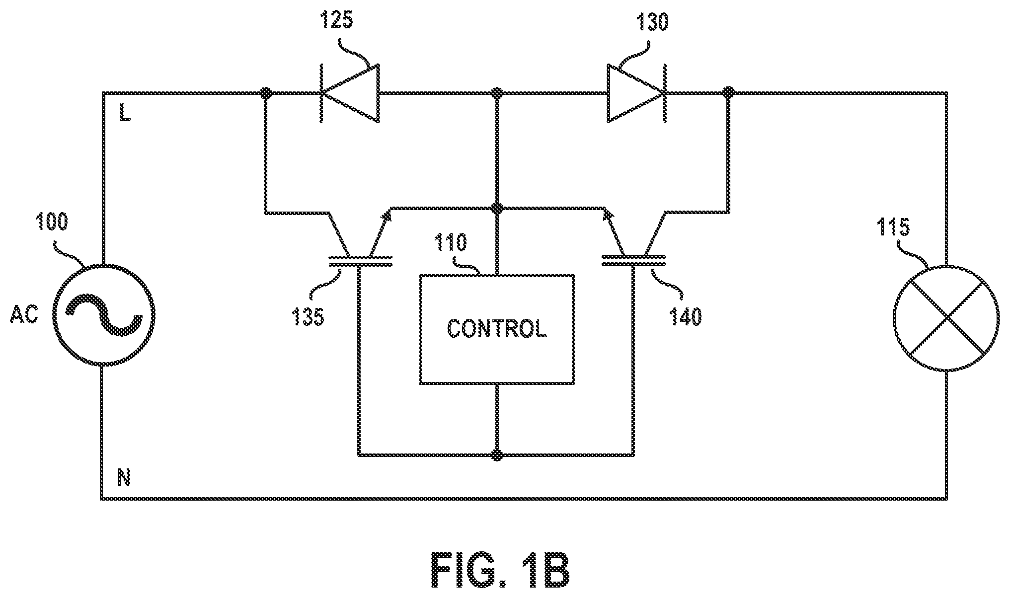
FIGS. 1A, 1B, and 1C schematically illustrate prior art circuit interrupters.
FIG. 2 schematically illustrates a solid-state circuit interrupter according to one or more aspects of the present invention.
FIG. 3 schematically illustrates a solid-state circuit interrupter according to one or more aspects of the present invention.
FIG. 4 schematically illustrates a solid-state circuit interrupter according to one or more aspects of the present invention.
FIG. 5 schematically illustrates a solid-state circuit interrupter according to one or more aspects of the present invention.
DETAILED DESCRIPTION
A circuit interrupter positioned between a supply circuit and a load circuit includes a fault detection circuit that senses wave forms to the load circuit, a fault processing circuit that detects the presence of a fault and generates a fault output signal when a fault detected, and a control circuit switch connected to the fault processing circuit, wherein the control circuit switch is activated in response to the fault output signal, thus isolating the load circuit from the supply circuit.
In some embodiments, a circuit interrupter is optically linked to a control circuit, such that when a fault is detected, an optical control circuit switch of the circuit interrupter is activated by an optical signal, thus isolating load circuit from the supply circuit.
A circuit interrupter can be coupled to another circuit interrupter via a power distribution control unit, wherein the power distribution control unit may be configured, optionally, to be managed remotely via automated control interface.
FIGS. 1A, 1B, and 1C schematically illustrate various embodiments of the prior art, none of which have an optical coupling. FIG. 2 is one example of a double pole, single throw circuit interrupter. FIG. 3 is one example of a double pole, single throw circuit interrupter with a "pseudo air gap switch" (alternatively referred to as an "Amber crowbar"). FIG. 4 is one example of a single pole, single throw circuit interrupter. FIG. 5 is one example of a double pole, double throw circuit interrupter.
As used herein, a fault detection circuit sensing waveforms includes the ability to sense over-current conditions, over-voltage conditions, including ground-fault and arc-fault conditions, and then signal which condition is faulting. In addition, when the control circuit switch is opened by the presence of a fault processing signal output thus isolating the load circuit from the supply circuit in some embodiments the control circuit is not isolated from the supply circuit. In the embodiments where a constant optical signal is required, the control circuit is not isolated from the supply circuit when the optical signal is not present. One knowledgeable in the art understands the need for and why a lock-out/tag-out capability is required.
FIG. 1A schematically illustrates a simple power controller. In this art, power is controlled by the controller 110 which controls a TRIAC 105. When released by the source 100, the controller 110 may allow the power through by activating the TRIAC 105 or not, thus allowing power to flow to load 115 or not.
FIG. 1B schematically illustrates a circuit interrupter in which the controller 110 controls the flow of electricity by controlling two solid state bipolar junction transistors 135 and 140 through a connection to the base terminals of the bipolar junction transistors 135 and 140. These two power BJT's 135 and 140 allow for the power from source 100 to flow through them to power the load circuit 115. Each BJT 135 and 140 has a diode connected in parallel with it, wherein the BJT 135 is connected in parallel with diode 125, and the BJT 140 is connected in parallel with diode 130.
FIG. 1C schematically illustrates a circuit interrupter which utilizes two power MOSFETs 145 and 150. Here, the power flows from the source 100 through the MOSFET 145 when the controller turns the MOSFET 145 on and the wave is in the positive part of its cycle. The wave then moves through the diode 130 and the power is then transferred to the load 115. In the negative part of the power cycle, the controller 110 turns the MOSFET 150 on so that power will flow through the MOSFET 150 and the diode 125. The diodes 125 and 130 in FIG. 1C represent internal parasitic diodes of the MOSFETs 145 and 150, respectively, and are illustrated to show functionality. Diodes may also be physically added, but doing so is unneeded.
FIG. 2 schematically illustrates an exemplary embodiment of a Double Pole Single Throw circuit interrupter. FIG. 2 illustrates an AC source 200, two power MOSFETs 220 and 250 which are connected to respective controllers 230 and 240, a load 270, and two diodes 210 and 260 which represent internal parasitic diodes of the MOSFETs 220 and 250, respectively.
The embodiment features two controllers 230 and 240 which control the configuration of the circuit on either the positive or negative part of the wave emanating from the power source 200. On the positive part of the wave, the controller 230 sends a signal to the gate of the power MOSFET 220 turning the MOSFET 220 on. The wave travels through the MOSFET 220, through the load circuit 270 and returns to the source through the diode 260. On the negative part of the wave, the controller 240 turns the MOSFET 250 on through its gate. The wave then travels through the MOSFET 250, through the load circuit 270, and returns to the source 200 through the diode 210. FIG. 2 illustrates a method to greatly reduce the current flowing to the load but does not reduce the current flowing to load to 0. A true air gap circuit by definition would reduce the current to load to 0, therefore there is a need for improvement to the double pole single throw circuit.
FIG. 3 schematically illustrates a solid-state circuit interrupter which is similar to FIG. 2, but which further includes a pseudo airgap switch circuit (or the "Amber Crowbar") which is placed between the load and the double pole single throw circuit. The basic function of the pseudo airgap switch circuit is to short (or shunt) the load circuit 365 when the double pole single throw circuit is off, thus allowing any signal to bypass the load circuit 365 and protecting the load circuit 365 by reducing the current (e.g., leakage current) to the load to zero when the double pole single throw circuit is off. This improvement makes the solid-state power device have a true airgap without the introduction of electromechanical devices. The pseudo airgap switch circuit comprises a controller 355 which controls two power MOSFETs 340 and 360. When a problematic wave seeks to enter the load circuit, the "Amber Crowbar" circuit activates. On the positive wave cycle, the MOSFET 340 is activated by the controller 355. The wave passes through the MOSFET 340 and diode 350 and returns to the source 300 safely avoiding the load circuit 365. On the negative cycle, the MOSFET 360 is activated by the controller 355. The wave passes through the MOSFET 360 and diode 345 and returns to the source 300 safely avoiding the load circuit 365. As in other embodiments discussed herein, the diodes 345 and 350 represent internal parasitic diodes of the respective MOSFETs 340 and 360, but can include actual diode components, although doing so is redundant.
In some embodiments, a circuit interrupter is positioned between a supply circuit and a load circuit comprises a fault detection circuit sensing wave forms to the load circuit; a fault processing circuit for detecting the presence of a fault and generating a fault output signal when a fault is detected; and a control circuit switch connected to the fault processing signal output wherein the control circuit switch is opened by the presence of the fault output signal thus isolating the load circuit from the supply circuit; optionally a circuit interrupter has a fault processing circuit and the control circuit optically linked such that when a fault is detected the control circuit switch is opened by the optical fault output signal thus isolating the load circuit from the supply circuit; optionally a circuit interrupter is coupled to another circuit interrupter via a power distribution control unit; optionally a circuit interrupter comprises a power distribution control unit manageable remotely via an automated control interface.
In some embodiments a circuit interrupter positioned between a supply circuit and a load circuit comprises a fault detection circuit sensing wave forms to the load circuit; a fault processing circuit for detecting the presence of a fault and generating an optical fault output signal when a fault is detected; and a control circuit switch optically connected to the fault processing signal output wherein the switch is opened by the presence of the fault output signal isolating the load circuit from the supply circuit; optionally, a circuit interrupter is coupled to another circuit interrupter via a power distribution control unit; optionally, a circuit interrupter is coupled to a power distribution control unit manageable remotely via an automated control interface.
In some embodiments a circuit interrupter method comprises the steps of sensing by a fault detection circuit wave forms to a load circuit; of detecting by a fault processing circuit presence of a fault; and of generating by the fault processing circuit an optical fault output signal when a fault is detected; wherein a control circuit switch is optically connected to the fault processing signal output, such that the switch is opened by the presence of the fault output signal isolating the load circuit from a supply circuit; optionally, the step of coupling to another circuit interrupter via a power distribution control unit; optionally, the power distribution control unit is manageable remotely via an automated control interface.
In some embodiments a circuit interrupter positioned between a supply circuit and a load circuit comprises a fault detection circuit sensing wave forms to the load circuit; a fault processing circuit for detecting the presence of a fault and generating a fault output signal when a fault is detected; and wherein the fault processing circuit and the control circuit must be optically linked for continuous operation such that when a fault is detected the control circuit switch is opened by the absence of an optical signal thus isolating the load circuit from the supply circuit; optionally, a circuit interrupter comprises a fault processing circuit and control circuit optically linked but physically separated from each other such that a physical object may be inserted between them blocking the optical link; optionally, a circuit interrupter comprises a physical object is a portion of a lock-out/tag-out mechanism that is configured to render the circuit interrupter in a state wherein current can not flow from the supply circuit to the load circuit.
In some embodiments an apparatus comprises a plurality of circuit interrupters, each positioned between a supply circuit and a load circuit wherein the apparatus comprises a power distribution control unit and is manageable remotely via an automated control interface.
FIG. 4 schematically illustrates a solid-state circuit interrupter according to an exemplary embodiment. For example, FIG. 4 illustrates an exemplary embodiment for implementing a controller as shown in the embodiments of FIGS. 2 and 3. In the exemplary embodiment of FIG. 4, the control block comprises a source connection 400, a load 460, MOSFETS 425 and 455, internal parasitic diodes 475 and 480 of the MOSFETs 425 and 455, respectively, two diodes 405 and 420, a voltage reference that is generated by a Zener diode 470 and a capacitor 430. Additionally, there are 4 resistors 410, 415, 465 and 435. An operational amplifier 440 is connected to a BJT 445 which is mirrored to an optically controlled phototransistor 450 all of which control the operation of the MOSFET 425 and MOSFET 455. FIG. 5 schematically illustrates a solid-state circuit interrupter according to another exemplary embodiment. For example, FIG. 5 illustrates another exemplary embodiment for implementing a controller as shown in the embodiments of FIGS. 2 and 3. The embodiment of FIG. 5 comprises 4 diodes 510, 520, 570 and 597, two MOSFETs 525 and 575, a BJT 540, and a phototransistor 545. The embodiment of FIG. 5 further comprises two Zener diodes 555 and 590 that are connected in parallel with respective capacitors 560 and 585, to provide clamping circuits that generate voltage references to drive the MOSFETs 525 and 575. Finally, there is an operational amplifier 535 which functions as a controller for the BJT 540. Additionally, one embodiment may include a programable chip inside of the controller for further control over the power functions.
The controller's main function is to convert AC power to DC by using of switching. This process starts with the configuration of the controller by applying a photo source to phototransistor 545. The optical signal (denoted by the arrows directed to the phototransistor 545) can enter through a device such as a connected fiber optics cable, but other methods and devices work as well. Optionally, the phototransistor 545 can be replaced by a more typical power BJT, but the preferred embodiment includes the phototransistor 545.
When turned on, the optical transistor 545 stays on until the rest of the controller is set. Essentially, the phototransistor 545 begins an initialization state for a few cycles of applied AC power around a few hundred milliseconds, but this can be tuned for faster or slower startup speeds. With the addition of an optional control block, the optical transistor 545 can be used as a means for control of the controller or other added function with use of control blocks.
This process starts with the AC source 500 emitting power. On the positive part of the cycle, the wave travels to the first node marked 505. Then, the wave enters the diode 510 and passes over resistor 515. Next, the wave begins to charge the capacitor 585 and Zener diode 590 pair after passing over resistor 580. This pair functions as a gate driver which will turn the power MOSFET 575 on for the next cycle. On the negative part of the first cycle, the wave passes over the diode 570 and the resistor 565 to charge the Zener diode 555 and the capacitor 560 pair, which like the other pair functions as a gate source driver to drive the power MOSFET 525. Additionally, this negative part of the wave enters the comparator 535 serving as the V- for proper comparator function.
The next cycle begins with each of the power MOSFETS 525 and 575 turned on. The positive cycle of the wave is first. Here, the wave passes through the MOSFET 525 and then across the resistor 530. The voltage across the resistor 530 is measured by the comparator 535. If the voltage closest to the MOSFET is less than the voltage of that at the rightmost end of the resistor 530, the comparator 535 turns on and effectively clamps the circuit by turning on the BJT 540, resulting in shunting the current away from the load and deactivating the MOSFET 525. If the wave is not shunted, then it begins entering the load 595. The wave then exits the load 595 and enters the anode of the diode 597 and exits the cathode and returns to the source 500.
On the negative part of the wave, the wave passes through the MOSFET 575, enters the load 595, and then exits it. Then, the wave enters the anode of diode 520 exits the cathode and returns to the source.
The overall function of the circuit allows for controlled delivery of power to the load 595 with control along the way by means of the operational amplifier 535 and the phototransistor 545.
Foregoing descriptions of specific embodiments of the invention have been presented for purposes of illustration and description. They are not intended to be exhaustive or to limit the invention to the precise forms disclosed. Modifications and variations are possible in light of the above teaching. The embodiments were chosen and described in order to explain the principles and the application of the invention, thereby enabling others skilled in the art to utilize the invention in its various embodiments and modifications according to the particular purpose contemplated. The scope of the invention is intended to be defined by the claims appended hereto and their equivalents.
* * * * *
References
-
adweek.com/tv-video/the-new-york-times-can-now-predict-your-emotions-and-motivations-after-reading-a-story
-
samy.pl/evercookie
-
wyden.senate.gov/news/press-releases/wyden-releases-discussion-draft-of-legislation-to-provide-real-protections-for-americans-privacy
-
rubio.senate.gov/public/index.cfm/2019/1/rubio-introduces-privacy-bill-to-protect-consumers-while-promoting-innovation#:%7E:text=Washingt%E2%80%A6
D00000
D00001
D00002
D00003
D00004
D00005
D00006
D00007
XML
uspto.report is an independent third-party trademark research tool that is not affiliated, endorsed, or sponsored by the United States Patent and Trademark Office (USPTO) or any other governmental organization. The information provided by uspto.report is based on publicly available data at the time of writing and is intended for informational purposes only.
While we strive to provide accurate and up-to-date information, we do not guarantee the accuracy, completeness, reliability, or suitability of the information displayed on this site. The use of this site is at your own risk. Any reliance you place on such information is therefore strictly at your own risk.
All official trademark data, including owner information, should be verified by visiting the official USPTO website at www.uspto.gov. This site is not intended to replace professional legal advice and should not be used as a substitute for consulting with a legal professional who is knowledgeable about trademark law.