Anode structure for solid-state lithium-based thin-film battery
de Souza , et al. March 9, 2
U.S. patent number 10,944,128 [Application Number 15/474,668] was granted by the patent office on 2021-03-09 for anode structure for solid-state lithium-based thin-film battery. This patent grant is currently assigned to International Business Machines Corporation. The grantee listed for this patent is International Business Machines Corporation. Invention is credited to Joel P. de Souza, Yun Seog Lee, Devendra K. Sadana.


| United States Patent | 10,944,128 |
| de Souza , et al. | March 9, 2021 |
Anode structure for solid-state lithium-based thin-film battery
Abstract
A solid-state lithium-based battery is provided in which the formation of lithium islands (i.e., lumps) during a charging/recharging cycle is reduced, or even eliminated. Reduction or elimination of lithium islands (i.e., lumps) can be provided by forming a lithium nucleation enhancement liner between a lithium-based solid-state electrolyte layer and a top electrode of a solid-state lithium based battery.
| Inventors: | de Souza; Joel P. (Putnam Valley, NY), Lee; Yun Seog (White Plains, NY), Sadana; Devendra K. (Pleasantville, NY) | ||||||||||
|---|---|---|---|---|---|---|---|---|---|---|---|
| Applicant: |
|
||||||||||
| Assignee: | International Business Machines
Corporation (Armonk, NY) |
||||||||||
| Family ID: | 1000005414369 | ||||||||||
| Appl. No.: | 15/474,668 | ||||||||||
| Filed: | March 30, 2017 |
Prior Publication Data
| Document Identifier | Publication Date | |
|---|---|---|
| US 20180287130 A1 | Oct 4, 2018 | |
| Current U.S. Class: | 1/1 |
| Current CPC Class: | H01M 4/0447 (20130101); H01M 10/0436 (20130101); H01M 10/049 (20130101); H01M 10/0525 (20130101); H01M 10/0585 (20130101); H01M 10/052 (20130101); H01M 50/24 (20210101); H01M 10/0562 (20130101); H01M 2300/0068 (20130101); H01M 4/525 (20130101); H01M 2220/30 (20130101) |
| Current International Class: | H01M 10/05 (20100101); H01M 10/0585 (20100101); H01M 10/0562 (20100101); H01M 10/052 (20100101); H01M 10/04 (20060101); H01M 4/04 (20060101); H01M 10/0525 (20100101); H01M 4/525 (20100101) |
References Cited [Referenced By]
U.S. Patent Documents
| 4369237 | January 1983 | Goebel |
| 5939217 | August 1999 | Tamura et al. |
| 5994834 | November 1999 | Alwan et al. |
| 6495283 | December 2002 | Yoon et al. |
| 8236452 | August 2012 | Zhamu et al. |
| 8383265 | February 2013 | Kang et al. |
| 8790804 | July 2014 | Deligianni et al. |
| 8999571 | April 2015 | Chiang et al. |
| 2001/0032666 | October 2001 | Jenson et al. |
| 2002/0071983 | June 2002 | Rowen et al. |
| 2002/0092558 | July 2002 | Kim et al. |
| 2004/0131779 | July 2004 | Haubrich et al. |
| 2004/0131925 | July 2004 | Jenson |
| 2004/0166409 | August 2004 | Takada |
| 2005/0064291 | March 2005 | Sato et al. |
| 2005/0147877 | July 2005 | Tarnowski |
| 2005/0191547 | September 2005 | Konishiike |
| 2008/0057397 | March 2008 | Skotheim |
| 2008/0213671 | September 2008 | Kogetsu et al. |
| 2009/0246636 | October 2009 | Chiang et al. |
| 2009/0258295 | October 2009 | Niessen et al. |
| 2011/0076542 | March 2011 | Farmer |
| 2011/0095720 | April 2011 | Shacklette et al. |
| 2011/0143195 | June 2011 | Ito et al. |
| 2011/0281160 | November 2011 | Doi |
| 2011/0294015 | December 2011 | Pirk et al. |
| 2012/0270114 | October 2012 | Reynolds |
| 2013/0089769 | April 2013 | Proctor et al. |
| 2013/0095381 | April 2013 | Oukassi et al. |
| 2013/0130066 | May 2013 | Pytlik et al. |
| 2013/0149593 | June 2013 | Hayashi et al. |
| 2013/0260183 | October 2013 | Ellis-Monaghan et al. |
| 2014/0212735 | July 2014 | Li et al. |
| 2015/0084157 | March 2015 | Tegen et al. |
| 2015/0280198 | October 2015 | Weis et al. |
| 2016/0329541 | November 2016 | Adams et al. |
| 2017/0162854 | June 2017 | Sugiura |
| 2019/0088991 | March 2019 | Hegde |
| 101507024 | Aug 2009 | CN | |||
| 101771168 | Jul 2010 | CN | |||
| 102301518 | Dec 2011 | CN | |||
| 104205467 | Dec 2014 | CN | |||
| 105489845 | Apr 2016 | CN | |||
| 102011085863 | May 2013 | DE | |||
| 2014143008 | Aug 2014 | JP | |||
| 2015026555 | Feb 2015 | JP | |||
| 1020070077231 | Jul 2007 | KR | |||
| 100855081 | Aug 2008 | KR | |||
| 2017105234 | Jun 2017 | WO | |||
Other References
|
"Fuse", Merriam-Webster.com, Web, Aug. 9, 2018, 1 page. cited by applicant . Office Action dated Aug. 16, 2018 received in a related U.S. Patent Application, namely U.S. Appl. No. 15/481,042. cited by applicant . List of IBM Patents or Patent Applications Treated as Related, dated Nov. 22, 2017, 2 pages. cited by applicant . Zeng, et al., "In situ TEM study of the Li--Au reaction in an electrochemical liquid cell", Faraday Discuss., Jul. 2014, pp. 95-107, 176. cited by applicant . Yan, et al., "Selective deposition and stable encapsulation of lithium through heterogeneous seeded growth", Nature Energy, Feb. 22, 2016, pp. 1-9, Article No. 16010. cited by applicant . Office Action dated Feb. 8, 2019 received in U.S. Appl. No. 15/481,042, Copy Not Enclosed. cited by applicant . Office Action dated Feb. 26, 2019 received in U.S. Appl. No. 15/818,385, Copy Not Enclosed. cited by applicant . Office Action dated Feb. 28, 2019 received in U.S. Appl. No. 15/818,405, Copy Not Enclosed. cited by applicant . Office Action dated Oct. 5, 2018 received in U.S. Appl. No. 15/818,405. cited by applicant . Office Action dated Oct. 5, 2018 received in U.S. Appl. No. 15/818,385. cited by applicant . Office Action dated May 16, 2019 received in U.S. Appl. No. 15/818,350. cited by applicant . Office Action dated May 16, 2019 received in U.S. Appl. No. 15/818,286. cited by applicant . Office Action dated Jun. 5, 2019 received in U.S. Appl. No. 15/818,405. cited by applicant . Office Action dated Jun. 11, 2019 received in U.S. Appl. No. 15/481,042. cited by applicant . Office Action dated Jul. 10, 2019 received in U.S. Appl. No. 15/818,385, Copy Not Enclosed. cited by applicant . Office Action dated Nov. 14, 2019 received in U.S. Appl. No. 15/820,609, copy not enclosed. cited by applicant . International Search Report with the Written Opinion dated Jun. 21, 2018 received in a corresponding foreign application, 9 pages. cited by applicant . Office Action dated Aug. 20, 2020 received in U.S. Appl. No. 15/820,609, Copy Not Enclosed. cited by applicant. |
Primary Examiner: Ruddock; Ula C
Assistant Examiner: Chuo; Tony S
Attorney, Agent or Firm: Scully, Scott, Murphy & Presser, P.C. Kelly, Esq.; L. Jeffrey
Claims
What is claimed is:
1. A solid-state lithium-based battery comprising: a bottom electrode; a battery material stack located only on a portion of the bottom electrode, wherein the battery material stack includes a lithiated cathode material layer, a lithium-based solid-state electrolyte layer located on the lithiated cathode material layer, and an anode structure consisting of a lithium nucleation enhancement liner composed of a titanium-zirconium-molybdenum alloy (TZM), and a lithium accumulation region composed of lithium nucleated by the lithium nucleation enhancement liner during a charging process, wherein the lithium accumulation region is located on a topmost surface of the lithium nucleation enhancement liner that is opposite a bottommost surface of the lithium nucleation enhancement liner that forms an interface directly with the lithium-based solid-state electrolyte; a top electrode located on a topmost surface of the battery material stack; and an air and/or moisture impermeable structure located directly on other portions of the bottom electrode not containing the battery material stack, wherein the air and/or moisture impermeable structure directly contacts an entirety of an outermost sidewall of the battery material stack and directly contacts a portion of a topmost surface of the top electrode.
2. The solid-state lithium-based battery of claim 1, wherein the lithiated cathode material layer, the lithium-based solid-state electrolyte layer, and the lithium nucleation enhancement liner have sidewall surfaces that are vertically aligned with each other.
3. The solid-state lithium-based battery of claim 2, wherein the top electrode has sidewall surfaces that are vertically aligned to the sidewall surfaces of the lithiated cathode material layer, the lithium-based solid-state electrolyte layer, and the lithium nucleation enhancement liner.
4. The solid-state lithium-based battery of claim 1, wherein the lithiated cathode material layer is composed of LiCoO.sub.2, and the lithium-based solid-state electrolyte layer is composed of LiPON.
5. The solid-state lithium-based battery of claim 1, wherein the lithium accumulation region is continuously located on the topmost surface of the lithium nucleation enhancement liner.
6. The solid-state lithium-based battery of claim 1, wherein the lithium accumulation region is discontinuously located on the topmost surface of the lithium nucleation enhancement liner.
7. The solid-state lithium-based battery of claim 1, further comprising a substrate located beneath the bottom electrode.
8. The solid-state lithium-based battery of claim 1, wherein the battery has a charge rate of greater than 3 C, wherein C is the total battery capacity per hour.
9. The solid-state lithium-based battery of claim 1, wherein the battery has a thickness of 100 .mu.m or less.
10. A solid-state lithium-based battery comprising: a bottom electrode; a battery material stack located on a surface of the bottom electrode, wherein the battery material stack includes a lithiated cathode material layer, a lithium-based solid-state electrolyte layer located on the lithiated cathode material layer, and an anode structure consisting of a lithium nucleation enhancement liner composed of a titanium-zirconium-molybdenum alloy (TZM), a first lithium accumulation region composed of lithium nucleated by the lithium nucleation enhancement liner during a charging process located on a bottommost surface of the lithium nucleation enhancement liner, and a second lithium accumulation region composed of lithium nucleated by the lithium nucleation enhancement liner during the charging process located on a topmost surface of the lithium nucleation enhancement liner; a top electrode located on a topmost surface of the battery material stack; and an air and/or moisture impermeable structure located directly on other portions of the bottom electrode not containing the battery material stack, wherein the air and/or moisture impermeable structure directly contacts an entirety of an outermost sidewall of the battery material stack and directly contacts a portion of a topmost surface of the top electrode.
11. A solid-state lithium-based battery comprising: a bottom electrode; a battery material stack located a surface of the bottom electrode, wherein the battery material stack includes a lithiated cathode material layer, a lithium-based solid-state electrolyte layer located on the lithiated cathode material layer, and a lithium nucleation enhancement liner, wherein the lithium nucleation enhancement liner is composed of a titanium-zirconium-molybdenum alloy (TZM); and a top electrode located on the lithium nucleation enhancement liner of the battery material stack.
Description
BACKGROUND
The present application relates to an all solid-state thin-film battery and a method of forming the same. More particularly, the present application relates to a solid-state lithium-based thin-film battery in which lithium lump formation during a charging/recharging cycle is reduced and a method of forming such a thin-film battery.
In recent years, there has been an increased demand for portable electronic devices such as, for example, computers, mobile phones, tracking systems, scanners, medical devices, smart watches, and fitness devices. One drawback with portable electronic devices is the need to include a power supply within the device itself. Typically, a battery is used as the power supply of such portable electronic devices. Batteries must have sufficient capacity to power the portable electronic device for at least the length that the device is being used. Sufficient battery capacity can result in a power supply that is quite heavy and/or large compared to the rest of the portable electronic device. As such, smaller sized and lighter weight power supplies with sufficient energy storage are desired. Such power supplies can be implemented in smaller and lighter weight portable electronic devices.
Another drawback of conventional batteries is that some of the batteries contain potentially flammable and toxic materials that may leak and may be subject to governmental regulations. As such, it is desired to provide an electrical power supply that is safe, solid-state and rechargeable over many charge/discharge life cycles.
One type of an energy-storage device that is small and light weight, contains non-toxic materials and that can be recharged over many charge/discharge cycles is a solid-state, lithium-based battery. Lithium-based batteries are rechargeable batteries that include two electrodes implementing lithium. Some challenges facing conventional solid-state, lithium-based batteries include, for example, volume expansion and/or deformation during cycling, and/or mechanical failure in the thin-film battery due to usable-lithium loss.
Moreover, in conventional solid-state, lithium-based batteries, a high interfacial energy can exist between metallic lithium and the top electrode. Also, localized lithium islands (i.e., lumps) can accumulate instead of a continuous and uniform lithium layer which may facilitate deformation of the electrode and the solid-state electrolyte layer and, can ultimately lead to crack formation within the thin-film battery. As such, there is a need for providing a solid-state, lithium-based battery which has a low interfacial energy between the metallic lithium and top electrode and which can reduce, and in some instances, even eliminate the formation of localized lithium islands (i.e., lumps).
SUMMARY
A solid-state lithium-based battery is provided in which the formation of lithium islands (i.e., lumps) during a charging/recharging cycle is reduced, or even eliminated. The solid-state lithium-based battery of the present application is a thin-film battery that is small and light weight. The term "thin-film battery" is used throughout the present application to denote a battery whose thickness is 100 .mu.m or less. Reduction or elimination of lithium islands (i.e., lumps) can be provided by forming a lithium nucleation enhancement liner between a lithium-based solid-state electrolyte layer and a top electrode of a solid-state lithium based battery.
In one aspect of the present application, a solid-state lithium-based battery is provided. In one embodiment, the solid-state lithium-based battery may include a bottom electrode. A battery material stack is located on a surface of the bottom electrode. The battery material stack includes a lithiated cathode material layer, a lithium-based solid-state electrolyte layer located on the lithiated cathode material layer, and a lithium nucleation enhancement liner located on the lithium-based solid-state electrolyte layer. A top electrode is located on the lithium nucleation enhancement liner of the battery material stack. During charging/recharging, a lithium accumulation region is formed on at least one surface of the lithium nucleation enhancement liner.
In another aspect of the present application, a method of forming a solid-state lithium-based battery is provided. In one embodiment, the method may include forming a patterned sacrificial material on a surface of a bottom electrode, wherein the patterned sacrificial material contains an opening that physically exposes a portion of the surface of the bottom electrode. Next, a lithiated cathode material layer is formed on the patterned sacrificial material and on the physically exposed portion of the surface of the bottom electrode in the opening. A lithium-based solid-state electrolyte layer is then formed on the lithiated cathode material layer, and thereafter a lithium nucleation enhancement liner is formed on the lithium-based solid-state electrolyte layer, and a top electrode is formed on the lithium nucleation enhancement liner. Next, a lift-off process is performed to remove the patterned sacrificial material and materials formed on the patterned sacrificial material from the bottom electrode, while maintaining a material stack on the physically exposed portion of the surface of the bottom electrode. The material stack includes a remaining portion of each of the lithiated cathode material layer, the lithium-based solid-state electrolyte layer, the lithium nucleation enhancement liner and the top electrode. During a charging/recharging process, a lithium accumulation region is formed on at least one surface of the lithium nucleation enhancement liner.
BRIEF DESCRIPTION OF SEVERAL VIEWS OF THE DRAWINGS
FIG. 1 is a cross sectional view of an exemplary structure including a bottom electrode located on a surface of a substrate that can be employed in accordance with an embodiment of the present application.
FIG. 2 is a cross sectional view of the exemplary structure of FIG. 1 after forming a patterned sacrificial material on the surface of the bottom electrode, wherein the patterned sacrificial material includes an opening that physically exposes a portion of the surface of the bottom electrode.
FIG. 3 is a cross sectional view of the exemplary structure of FIG. 2 after forming a lithiated cathode material layer on the patterned sacrificial material and on the physically exposed portion of the bottom electrode in the opening.
FIG. 4 is a cross sectional view of the exemplary structure of FIG. 3 after forming a lithium-based solid-state electrolyte layer on the lithiated cathode material layer.
FIG. 5 is a cross sectional view of the exemplary structure of FIG. 4 after forming a lithium nucleation enhancement liner on the lithium-based solid-state electrolyte layer.
FIG. 6 is a cross sectional view of the exemplary structure of FIG. 5 after forming a top electrode on the lithium nucleation enhancement liner.
FIG. 7 is a cross sectional view of the exemplary structure of FIG. 6 after performing a lift-off process in which the patterned sacrificial material and all materials formed thereon are removed from the bottom electrode, while maintaining a material stack on the bottom electrode.
FIG. 8 is a cross sectional view of the exemplary structure of FIG. 7 after forming an air and/or moisture impermeable structure.
FIG. 9 is a cross sectional view after charging the resultant structure shown in FIG. 8.
DETAILED DESCRIPTION
The present application will now be described in greater detail by referring to the following discussion and drawings that accompany the present application. It is noted that the drawings of the present application are provided for illustrative purposes only and, as such, the drawings are not drawn to scale. It is also noted that like and corresponding elements are referred to by like reference numerals.
In the following description, numerous specific details are set forth, such as particular structures, components, materials, dimensions, processing steps and techniques, in order to provide an understanding of the various embodiments of the present application. However, it will be appreciated by one of ordinary skill in the art that the various embodiments of the present application may be practiced without these specific details. In other instances, well-known structures or processing steps have not been described in detail in order to avoid obscuring the present application.
It will be understood that when an element as a layer, region or substrate is referred to as being "on" or "over" another element, it can be directly on the other element or intervening elements may also be present. In contrast, when an element is referred to as being "directly on" or "directly over" another element, there are no intervening elements present. It will also be understood that when an element is referred to as being "beneath" or "under" another element, it can be directly beneath or under the other element, or intervening elements may be present. In contrast, when an element is referred to as being "directly beneath" or "directly under" another element, there are no intervening elements present.
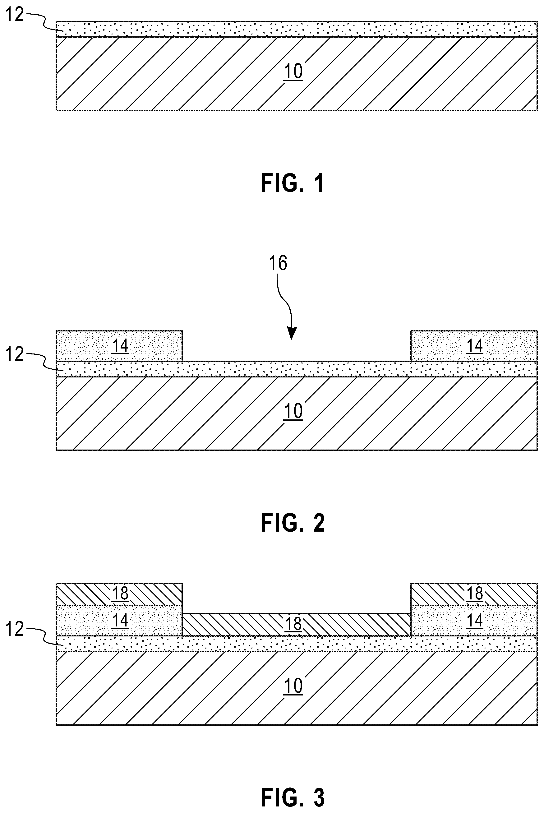
Referring first to FIG. 1, there is illustrated an exemplary structure that can be employed in accordance with an embodiment of the present application. The exemplary structure of FIG. 1 includes a bottom electrode 12 located on a surface of a substrate 10. As is shown, the bottom electrode 12 is typically a continuous layer (without any intentionally formed gaps or breaks) that is present on an entirety of the substrate 10.
The substrate 10 that can be employed in the present application includes any conventional material that is used as a substrate for a solid-state lithium-based battery. In one embodiment, the substrate 10 may include one or more semiconductor materials. The term "semiconductor material" is used throughout the present application to denote a material having semiconducting properties.
Examples of semiconductor materials that may be employed as substrate 10 include silicon (Si), germanium (Ge), silicon germanium alloys (SiGe), silicon carbide (SiC), silicon germanium carbide (SiGeC), III-V compound semiconductors or II-VI compound semiconductors. III-V compound semiconductors are materials that include at least one element from Group III of the Periodic Table of Elements and at least one element from Group V of the Periodic Table of Elements. II-VI compound semiconductors are materials that include at least one element from Group II of the Periodic Table of Elements and at least one element from Group VI of the Periodic Table of Elements.
In one embodiment, the semiconductor material that may provide substrate 10 is a bulk semiconductor substrate. By "bulk" it is meant that the substrate 10 is entirely composed of at least one semiconductor material, as defined above. In one example, the substrate 10 may be entirely composed of silicon. In some embodiments, the bulk semiconductor substrate may include a multilayered semiconductor material stack including at least two different semiconductor materials, as defined above. In one example, the multilayered semiconductor material stack may comprise, in any order, a stack of Si and a silicon germanium alloy.
In another embodiment, substrate 10 is composed of a topmost semiconductor material layer of a semiconductor-on-insulator (SOI) substrate. The SOI substrate would also include a handle substrate (not shown) including one of the above mentioned semiconductor materials, and an insulator layer (not shown) such as a buried oxide below the topmost semiconductor material layer.
In any of the embodiments mentioned above, the semiconductor material that may provide the substrate 10 may be a single crystalline semiconductor material. The semiconductor material that may provide the substrate 10 may have any of the well known crystal orientations. For example, the crystal orientation of the semiconductor material that may provide substrate 10 may be {100}, {110}, or {111}. Other crystallographic orientations besides those specifically mentioned can also be used in the present application.
In another embodiment, the substrate 10 is a metallic material such as, for example, aluminum (Al), aluminum alloy, titanium (Ti), tantalum (Ta), tungsten (W), or molybdenum (Mo).
In yet another embodiment, the substrate 10 is a dielectric material such as, for example, doped or non-doped silicate glass, silicon dioxide, or silicon nitride. In yet a further embodiment, the substrate 10 is composed of a polymer or flexible substrate material such as, for example, a polyimide, a polyether ketone (PEEK) or a transparent conductive polyester. In yet an even further embodiment, the substrate 10 may be composed of a multilayered stack of at least two of the above mentioned substrate materials, e.g., a stack of silicon and silicon dioxide.
The substrate 10 that can be used in the present application can have a thickness from 10 .mu.m to 5 mm. Other thicknesses that are lesser than, or greater than, the aforementioned thickness values may also be used for substrate 10.
In some embodiments, the substrate 10 may have a non-textured (flat or planar) surface. The term "non-textured surface" denotes a surface that is smooth and has a surface roughness on the order of less than 100 nm root mean square as measured by profilometry. In yet another embodiment, the substrate 10 may have a textured surface. In such an embodiment, the surface roughness of the textured substrate can be in a range from 100 nm root mean square to 100 .mu.m root mean square as also measured by profilometry. Texturing can be performed by forming a plurality of etching masks (e.g., metal, insulator, or polymer) on the surface of a non-textured substrate, etching the non-textured substrate utilizing the plurality of masks as an etch mask, and removing the etch masks from the non-textured surface of the substrate. In some embodiments, the textured surface of the substrate is composed of a plurality of pyramids. In yet another embodiment, the textured surface of the substrate is composed of a plurality of cones. In some embodiments, a plurality of metallic masks are used, which may be formed by depositing a layer of a metallic material and then performing an anneal. During the anneal, the layer of metallic material melts and balls-ups such that de-wetting of the surface of the substrate occurs.
The bottom electrode 12 may include any metallic electrode material such as, for example, titanium (Ti), platinum (Pt), nickel (Ni), aluminum (Al) or titanium nitride (TiN). In one example, the bottom electrode 12 includes a stack of, from bottom to top, titanium (Ti), platinum (Pt) and titanium (Ti). The bottom electrode 12 may be formed utilizing a deposition process including, for example, chemical vapor deposition (CVD), plasma enhanced chemical vapor deposition (PECVD), evaporation, sputtering, or plating. The bottom electrode 12 may have a thickness from 10 nm to 500 nm. Other thicknesses that are lesser than, or greater than, the aforementioned thickness values may also be used for the bottom electrode 12.
Referring now to FIG. 2, there is illustrated the exemplary structure of FIG. 1 after forming a patterned sacrificial material 14 on the surface of the bottom electrode 12, wherein the patterned sacrificial material 14 includes an opening 16 that physically exposes a portion of the surface of the bottom electrode 12. The opening 16 defines an area in which a solid-state lithium-based battery will be subsequently formed. Although the present application describes and illustrates a single opening 16, a plurality of openings 16 can be formed in which each opening of the plurality of openings 16 can define an area for subsequent formation of a solid-state lithium-based battery.
The patterned sacrificial material 14 can be formed by first applying a sacrificial material (not shown) to the physically exposed surface of the bottom electrode 12. In one embodiment, the sacrificial material is a photoresist material. In such an embodiment, the photoresist material may be a positive-tone photoresist material, a negative-tone photoresist material or a hybrid-tone photoresist material. The sacrificial material may be formed utilizing a deposition process such as, for example, spin-on coating or blade coating, followed by a bake step to evaporate any residual solvent(s). The sacrificial material may have a thickness from 100 nm to 20 .mu.m. Other thicknesses that are lesser than, or greater than, the aforementioned thickness values may also be used for the sacrificial material.
The deposited sacrificial material is then patterned. In one embodiment and when the sacrificial material is a photoresist material, the photoresist material may be patterned by exposing the photoresist material to a desired pattern of radiation, and thereafter the exposed photoresist material is developed utilizing a conventional resist developer to provide a patterned sacrificial material 14. When non-photoresist sacrificial materials are used, the non-photoresist sacrificial materials can be patterned by lithography and etching.
In another embodiment, the sacrificial material that provides the patterned sacrificial material 14 is a shadow mask. In such an embodiment, the shadow mask may be a pre-patterned metallic material or a pre-patterned polymeric material. The pre-patterned shadow mask material is attached to the structure shown in FIG. 1 by mechanical force or a removable adhesive.
Referring now to FIG. 3, there is illustrated the exemplary structure of FIG. 2 after forming a lithiated cathode material layer 18 on the patterned sacrificial material 14 and on the physically exposed portion of the bottom electrode 12 in the opening 16.
The lithiated cathode material layer 18 that can be employed in the present application includes a lithium-based mixed oxide. Examples of lithium-based mixed oxides that may be employed as the lithiated cathode material layer 18 include, but are not limited to, lithium cobalt oxide (LiCoO.sub.2), lithium nickel oxide (LiNiO.sub.2), lithium manganese oxide (LiMn.sub.2O.sub.4), lithium vanadium pentoxide (LiV.sub.2O.sub.5) or lithium iron phosphate (LiFePO.sub.4).
The lithiated cathode material layer 18 may be formed utilizing a deposition process such as, sputtering or plating. In one embodiment, the lithiated cathode material layer 18 is formed by sputtering utilizing any conventional precursor source material or combination of precursor source materials. In one example, a lithium precursor source material and a cobalt precursor source material are employed in forming a lithium cobalt mixed oxide. Sputtering may be performed in an admixture of an inert gas and oxygen. In such an embodiment, the oxygen content of the inert gas/oxygen admixture can be from 0.1 atomic percent to 70 atomic percent, the remainder of the admixture includes the inert gas. Examples of inert gases that may be used include argon, helium, neon, nitrogen or any combination thereof.
The lithiated cathode material layer 18 may have a thickness from 10 nm to 20 .mu.m. Other thicknesses that are lesser than, or greater than, the aforementioned thickness values may also be used for the lithiated cathode material layer 18.
Referring now to FIG. 4, there is illustrated the exemplary structure of FIG. 3 after forming a lithium-based solid-state electrolyte layer 20 on the lithiated cathode material layer 18. The lithium-based solid-state electrolyte layer 20 is a solid material that enables the conduction of lithium ions. Such materials may be electrically insulating or ionic conducting. Examples of materials that can be employed as the lithium-based solid-state electrolyte layer 20 include, but are not limited to, lithium phosphorus oxynitride (LiPON) or lithium phosphosilicate oxynitride (LiSiPON).
The lithium-based solid-state electrolyte layer 20 may be formed utilizing a deposition process such as, sputtering or plating. In one embodiment, the lithium-based solid-state electrolyte layer 20 is formed by sputtering utilizing any conventional precursor source material. Sputtering may be performed in the presence of at least a nitrogen-containing ambient. Examples of nitrogen-containing ambients that can be employed include, but are not limited to, N.sub.2, NH.sub.3, NH.sub.4, NO, or NH.sub.x wherein x is between 0 and 1. Mixtures of the aforementioned nitrogen-containing ambients can also be employed. In some embodiments, the nitrogen-containing ambient is used neat, i.e., non-diluted. In other embodiments, the nitrogen-containing ambient can be diluted with an inert gas such as, for example, helium (He), neon (Ne), argon (Ar) and mixtures thereof. The content of nitrogen (N.sub.2) within the nitrogen-containing ambient employed is typically from 10% to 100%, with a nitrogen content within the ambient from 50% to 100% being more typical.
The lithium-based solid-state electrolyte layer 20 may have a thickness from 10 nm to 10 .mu.m. Other thicknesses that are lesser than, or greater than, the aforementioned thickness values may also be used for the lithium-based solid-state electrolyte layer 20.
Referring now to FIG. 5, there is illustrated the exemplary structure of FIG. 4 after forming a lithium nucleation enhancement liner 22 on the lithium-based solid-state electrolyte layer 20. The lithium nucleation enhancement liner 22 is a continuous layer that covers the entirety of the lithium-based solid-state electrolyte layer 20. The lithium nucleation enhancement liner 22 includes a material that can facilitate the subsequent nucleation of lithium upon performing a charging/recharging process. In one embodiment, lithium nucleation enhancement liner 22 is composed of gold (Au), silver (Ag), zinc (Zn), magnesium (Mg), tantalum (Ta), tungsten (W), molybdenum (Mo), a titanium-zirconium-molybdenum alloy (TZM), or silicon (Si).
The lithium nucleation enhancement liner 22 can be formed utilizing a deposition process. Examples of deposition processes than can be used in forming the lithium nucleation enhancement liner 22 include chemical vapor deposition (CVD), plasma enhanced chemical vapor deposition (PECVD), evaporation, sputtering or plating. The lithium nucleation enhancement liner 22 has a thickness that is greater than 1 nm. In one embodiment, the lithium nucleation enhancement liner 22 has a thickness from 2 nm to 20 nm.
Referring now to FIG. 6, there is illustrated the exemplary structure of FIG. 5 after forming a top electrode 24 on the lithium nucleation enhancement liner 22. The top electrode 24 may include any metallic electrode material such as, for example, titanium (Ti), platinum (Pt), nickel (Ni), copper (Cu) or titanium nitride (TiN). In one example, the top electrode 24 includes a stack of, from bottom to top, nickel (Ni) and copper (Cu). In one embodiment, the metallic electrode material that provides the top electrode 24 may be the same as the metallic electrode material that provides the bottom electrode 12. In another embodiment, the metallic electrode material that provides the top electrode 24 may be different from the metallic electrode material that provides the bottom electrode 12. The top electrode 24 may be formed utilizing one of the deposition processes mentioned above for forming the bottom electrode 12. The top electrode 24 may have a thickness within the range mentioned above for the bottom electrode 12.
Referring now to FIG. 7, there is illustrated the exemplary structure of FIG. 6 after performing a lift-off process in which the patterned sacrificial material 14 and all materials formed thereon are removed from the bottom electrode 12, while maintaining a material stack on the bottom electrode 12. The material stack includes a remaining portion of each of the lithiated cathode material layer 18, the lithium-based solid-state electrolyte layer 20, the lithium nucleation enhancement liner 22 and the top electrode 24. The material stack is located on the physically exposed portion of the bottom electrode 12.
In one embodiment, the lift-off process includes removing the patterned sacrificial material 14 utilizing a solvent or etchant that is selective for removing the sacrificial material. In another embodiment, the removing does not include the use of a solvent, but instead, the mechanical force is released or release occurs by peeling the patterned sacrificial material 14 from the removable adhesive.
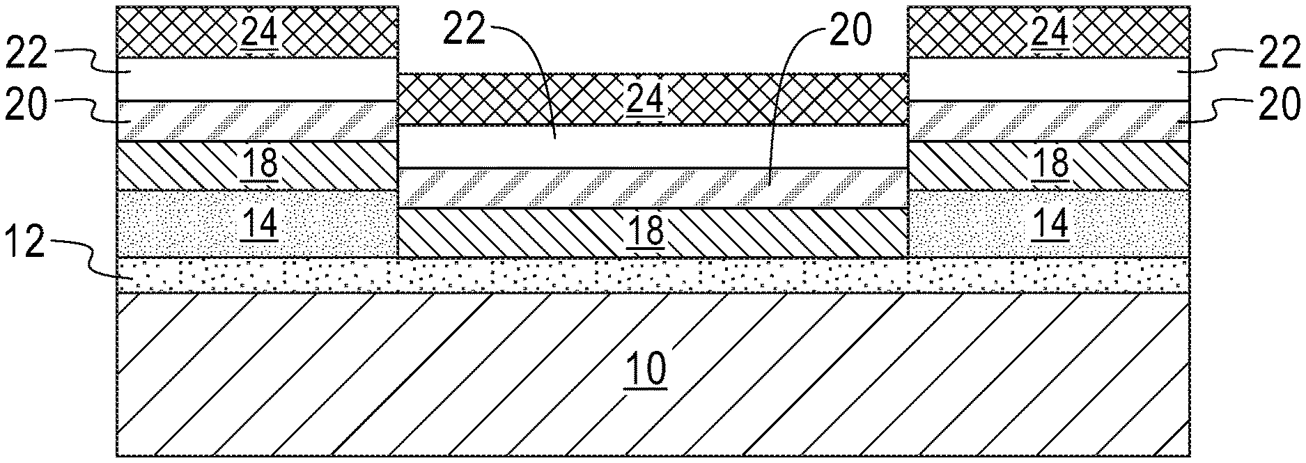
The exemplary structure shown in FIG. 7 illustrates a solid-state lithium-based battery in accordance with the present application. The solid-state lithium-based battery includes a bottom electrode 12, and a battery material stack (18, 20, 22) located on a portion of the surface of the bottom electrode 12. The battery material stack (18, 20, 22) includes lithiated cathode material layer 18, lithium-based solid-state electrolyte layer 20 located on the lithiated cathode material layer 18, and lithium nucleation enhancement liner 22. A top electrode 24 is located on the lithium nucleation enhancement liner 22 of the battery material stack (18, 20, 22). The solid-state lithium-based battery of the present application has a fast charge rate. In some embodiments, the solid-state lithium-based battery has a charge rate of greater than 3 C, wherein C is the total battery capacity per hour.
As shown in FIG. 7, the lithiated cathode material layer 18, the lithium-based solid-state electrolyte layer 22 and the lithium nucleation enhancement liner 22 of the solid-state lithium-based battery have sidewall surfaces that are vertically aligned with each other. As is further shown, the top electrode 24 of the solid-state lithium-based battery has sidewall surfaces that are vertically aligned to the sidewall surfaces of the lithiated cathode material layer 18, the lithium-based solid-state electrolyte layer 20, and the lithium nucleation enhancement liner 22 of the solid-state lithium-based battery.
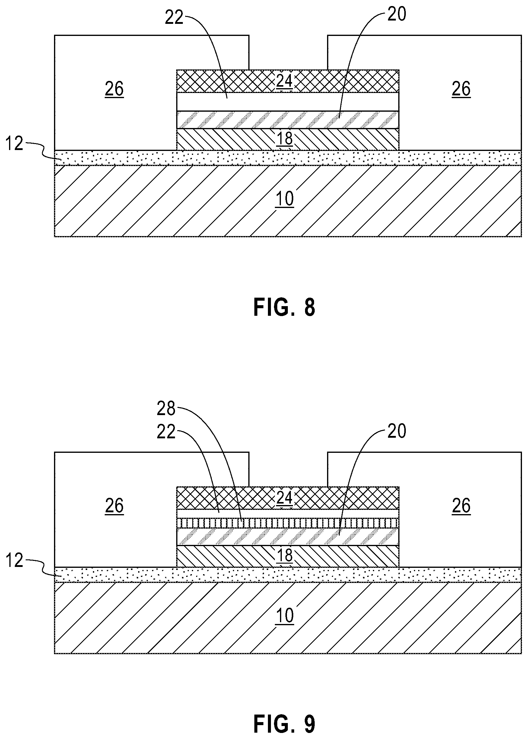
Referring now to FIG. 8, there is illustrated the exemplary structure of FIG. 7 after forming an air and/or moisture impermeable structure 26. The air and/or moisture impermeable structure 26 includes any air and/or moisture impermeable material or multilayered stack of such materials. Examples of air and/or moisture impermeable materials that can be employed in the present application include, but are not limited to, parylene, a fluoropolymer, silicon nitride, and/or silicon dioxide. The air and/or moisture impermeable structure 26 may be formed by first depositing the air and/or moisture impermeable material and thereafter patterning the air and/or moisture impermeable material. In one embodiment, patterning may be performed by lithography and etching.
The battery shown in FIG. 8 may now be subjected to a charging/recharging process. Charging/recharging may be performed utilizing conventional techniques well known to those skilled in the art. For example, the solid-state lithium-based battery of the present application can be charged/recharged by connecting the solid-state lithium-based battery of the present application to an external power supply.
During charging/recharging, a lithium accumulation region is formed on at least one (topmost and/or bottommost) surface of the lithium nucleation enhancement liner. In one example and as shown in FIG. 9, a lithium accumulation region 28 is formed between the lithium-based solid-state electrolyte layer 20 and the lithium nucleation enhancement liner 22 of the battery material stack (18, 20, 22) and the top electrode 24; during the charging/recharging process the thickness of the originally formed lithium-based solid-state electrolyte layer 20 and the lithium nucleation enhancement liner 22 may be reduced. Also and during the charging/recharging process, the lithium nucleation enhancement liner 22 may, or may not, be alloyed with some lithium. Collectively, the lithium accumulation region 28 and the lithium nucleation enhancement liner 22 provide an anode structure of the present application. In another example, not shown, but readily understood by one skilled in the art, a lithium accumulation region is formed between the lithium nucleation enhancement liner and the top electrode. In yet a further example, not shown, but readily understood by one skilled in the art, a first lithium accumulation region is formed between the lithium-based solid-state electrolyte layer and the lithium nucleation enhancement liner and a second lithium accumulation region is formed between the lithium nucleation enhancement liner and the top electrode.
In some embodiments, the lithium accumulation region 28 is continuously present on at least one surface of the lithium nucleation enhancement liner 22. In other embodiments (not shown), the lithium accumulation region 28 may exist as discrete islands, i.e., the lithium accumulation region 28 is discontinuously present on at least one surface of the lithium nucleation enhancement liner. In some embodiments, a first lithium accumulation region is continuously present on a first surface of the lithium nucleation enhancement liner, and a second lithium accumulation region is present as discrete islands on a second surface of the lithium nucleation enhancement liner. The density of these discrete islands is reduced, by as much as 80 percent or more, compared to a conventional solid-state lithium based battery that includes the same components except for the absence of the lithium nucleation enhancement liner 22.
While the present application has been particularly shown and described with respect to preferred embodiments thereof, it will be understood by those skilled in the art that the foregoing and other changes in forms and details may be made without departing from the spirit and scope of the present application. It is therefore intended that the present application not be limited to the exact forms and details described and illustrated, but fall within the scope of the appended claims.
* * * * *
D00000
D00001
D00002
D00003
D00004
XML
uspto.report is an independent third-party trademark research tool that is not affiliated, endorsed, or sponsored by the United States Patent and Trademark Office (USPTO) or any other governmental organization. The information provided by uspto.report is based on publicly available data at the time of writing and is intended for informational purposes only.
While we strive to provide accurate and up-to-date information, we do not guarantee the accuracy, completeness, reliability, or suitability of the information displayed on this site. The use of this site is at your own risk. Any reliance you place on such information is therefore strictly at your own risk.
All official trademark data, including owner information, should be verified by visiting the official USPTO website at www.uspto.gov. This site is not intended to replace professional legal advice and should not be used as a substitute for consulting with a legal professional who is knowledgeable about trademark law.