Apparatuses and methods for selective row refreshes
Bell , et al. February 23, 2
U.S. patent number 10,930,335 [Application Number 16/231,327] was granted by the patent office on 2021-02-23 for apparatuses and methods for selective row refreshes. This patent grant is currently assigned to Micron Technology, Inc.. The grantee listed for this patent is MICRON TECHNOLOGY, INC.. Invention is credited to Debra M. Bell, Brian P. Callaway, Jeff A. McClain.


| United States Patent | 10,930,335 |
| Bell , et al. | February 23, 2021 |
Apparatuses and methods for selective row refreshes
Abstract
Apparatuses and methods for selective row refreshes are disclosed herein. An example apparatus may include a refresh control circuit. The refresh control circuit may be configured to receive a target address associated with a target plurality of memory cells from an address bus. The refresh control circuit may further be configured to provide a proximate address to the address bus responsive, at least in part, to determining that a number of refresh operations have occurred. In some examples, a plurality of memory cells associated with the proximate address may be a plurality of memory cells adjacent the target plurality of memory cells.
| Inventors: | Bell; Debra M. (Dallas, TX), McClain; Jeff A. (Nampa, ID), Callaway; Brian P. (Boise, ID) | ||||||||||
|---|---|---|---|---|---|---|---|---|---|---|---|
| Applicant: |
|
||||||||||
| Assignee: | Micron Technology, Inc. (Boise,
ID) |
||||||||||
| Family ID: | 1000005379082 | ||||||||||
| Appl. No.: | 16/231,327 | ||||||||||
| Filed: | December 21, 2018 |
Prior Publication Data
| Document Identifier | Publication Date | |
|---|---|---|
| US 20190130961 A1 | May 2, 2019 | |
Related U.S. Patent Documents
| Application Number | Filing Date | Patent Number | Issue Date | ||
|---|---|---|---|---|---|
| 16160801 | Oct 15, 2018 | ||||
| 14707893 | Nov 20, 2018 | 10134461 | |||
| 14010120 | Jun 2, 2015 | 9047978 | |||
| Current U.S. Class: | 1/1 |
| Current CPC Class: | G11C 11/406 (20130101); G11C 7/1012 (20130101) |
| Current International Class: | G11C 11/406 (20060101); G11C 7/10 (20060101) |
| Field of Search: | ;365/222,149 |
References Cited [Referenced By]
U.S. Patent Documents
| 5299159 | March 1994 | Balistreri et al. |
| 5422850 | June 1995 | Sukegawa et al. |
| 5699297 | December 1997 | Yamazaki et al. |
| 5768196 | June 1998 | Bloker et al. |
| 5933377 | August 1999 | Hidaka |
| 5943283 | August 1999 | Wong et al. |
| 5970507 | October 1999 | Kato et al. |
| 6011734 | January 2000 | Pappert |
| 6061290 | May 2000 | Shirley |
| 6212118 | April 2001 | Fujita |
| 6310806 | October 2001 | Higashi et al. |
| 6424582 | July 2002 | Ooishi |
| 6434064 | August 2002 | Nagai |
| 6452868 | September 2002 | Fister |
| 6567340 | May 2003 | Nataraj et al. |
| 6950364 | September 2005 | Kim |
| 7027343 | April 2006 | Sinha et al. |
| 7057960 | June 2006 | Fiscus et al. |
| 7187607 | March 2007 | Koshikawa et al. |
| 7203115 | April 2007 | Eto et al. |
| 7209402 | April 2007 | Shinozaki et al. |
| 7215588 | May 2007 | Lee |
| 7444577 | October 2008 | Best et al. |
| 7551502 | June 2009 | Dono et al. |
| 7830742 | November 2010 | Han |
| 8451677 | May 2013 | Okahiro et al. |
| 8625360 | January 2014 | Iwamoto et al. |
| 8681578 | March 2014 | Narui |
| 8811100 | August 2014 | Ku |
| 8862973 | October 2014 | Zimmerman et al. |
| 8936573 | January 2015 | Greenfield et al. |
| 9032141 | May 2015 | Bains et al. |
| 9047978 | June 2015 | Bell et al. |
| 9058900 | June 2015 | Kang |
| 9087602 | July 2015 | Youn et al. |
| 9117544 | August 2015 | Bains et al. |
| 9123447 | September 2015 | Lee et al. |
| 9153294 | October 2015 | Kang |
| 9190139 | November 2015 | Jung et al. |
| 9286964 | March 2016 | Halbert et al. |
| 9299457 | March 2016 | Chun et al. |
| 9311985 | April 2016 | Lee et al. |
| 9324398 | April 2016 | Jones et al. |
| 9384821 | July 2016 | Bains et al. |
| 9412432 | August 2016 | Narui et al. |
| 9424907 | August 2016 | Fujishiro |
| 9484079 | November 2016 | Lee |
| 9514850 | December 2016 | Kim |
| 9570143 | February 2017 | Lim et al. |
| 9646672 | May 2017 | Kim et al. |
| 9672889 | June 2017 | Lee et al. |
| 9685240 | June 2017 | Park |
| 9691466 | June 2017 | Kim |
| 9697913 | July 2017 | Mariani et al. |
| 9741409 | August 2017 | Jones et al. |
| 9741447 | August 2017 | Akamatsu |
| 9747971 | August 2017 | Bains et al. |
| 9786351 | October 2017 | Lee et al. |
| 9799391 | October 2017 | Wei |
| 9805782 | October 2017 | Liou |
| 9805783 | October 2017 | Ito et al. |
| 9818469 | November 2017 | Kim et al. |
| 9865326 | January 2018 | Bains et al. |
| 9922694 | March 2018 | Akamatsu |
| 9934143 | April 2018 | Bains et al. |
| 9953696 | April 2018 | Kim |
| 10032501 | July 2018 | Ito et al. |
| 10083737 | September 2018 | Bains et al. |
| 10134461 | November 2018 | Bell et al. |
| 10147472 | December 2018 | Jones et al. |
| 10153031 | December 2018 | Akamatsu |
| 10170174 | January 2019 | Ito et al. |
| 10176860 | January 2019 | Mylavarapu |
| 10210925 | February 2019 | Bains et al. |
| 10297305 | May 2019 | Moon et al. |
| 10339994 | July 2019 | Ito et al. |
| 10387276 | August 2019 | Ryu et al. |
| 10600462 | March 2020 | Augustine et al. |
| 10600491 | March 2020 | Chou et al. |
| 10607686 | March 2020 | Akamatsu |
| 10629286 | April 2020 | Lee et al. |
| 10679710 | June 2020 | Hirashima et al. |
| 10770127 | September 2020 | Shore et al. |
| 2001/0008498 | July 2001 | Ooishi |
| 2002/0181301 | December 2002 | Takahashi et al. |
| 2003/0063512 | April 2003 | Takahashi et al. |
| 2003/0067825 | April 2003 | Shimano et al. |
| 2003/0090400 | May 2003 | Barker |
| 2003/0123301 | July 2003 | Jang et al. |
| 2003/0193829 | October 2003 | Morgan et al. |
| 2004/0008544 | January 2004 | Shinozaki et al. |
| 2004/0022093 | February 2004 | Lee |
| 2004/0114446 | June 2004 | Takahashi et al. |
| 2004/0130959 | July 2004 | Kawaguchi |
| 2004/0174757 | September 2004 | Garverick et al. |
| 2004/0184323 | September 2004 | Mori et al. |
| 2004/0218431 | November 2004 | Chung et al. |
| 2005/0105315 | May 2005 | Shin et al. |
| 2005/0243629 | November 2005 | Lee |
| 2006/0083099 | April 2006 | Bae et al. |
| 2006/0087903 | April 2006 | Riho et al. |
| 2006/0176744 | August 2006 | Stave |
| 2006/0262616 | November 2006 | Chen |
| 2007/0008799 | January 2007 | Dono et al. |
| 2007/0014174 | January 2007 | Ohsawa |
| 2007/0030746 | February 2007 | Best et al. |
| 2007/0133330 | June 2007 | Ohsawa |
| 2007/0297252 | December 2007 | Singh |
| 2008/0028260 | January 2008 | Oyagi et al. |
| 2008/0031068 | February 2008 | Yoo et al. |
| 2008/0126893 | May 2008 | Harrand et al. |
| 2008/0130394 | June 2008 | Dono et al. |
| 2008/0181048 | July 2008 | Han |
| 2008/0253212 | October 2008 | Iida et al. |
| 2008/0266990 | October 2008 | Loeffler |
| 2008/0316845 | December 2008 | Wang et al. |
| 2009/0077571 | March 2009 | Gara et al. |
| 2009/0161457 | June 2009 | Wakimoto |
| 2009/0185440 | July 2009 | Lee |
| 2009/0201752 | August 2009 | Riho et al. |
| 2009/0296510 | December 2009 | Lee et al. |
| 2010/0054011 | March 2010 | Kim |
| 2010/0074042 | March 2010 | Fukuda et al. |
| 2010/0080074 | April 2010 | Ohmaru et al. |
| 2010/0110809 | May 2010 | Kobayashi et al. |
| 2010/0110810 | May 2010 | Kobayashi |
| 2010/0131812 | May 2010 | Mohammad |
| 2010/0157693 | June 2010 | Iwai et al. |
| 2010/0329069 | December 2010 | Ito et al. |
| 2011/0026290 | February 2011 | Noda et al. |
| 2011/0069572 | March 2011 | Lee et al. |
| 2011/0216614 | September 2011 | Hosoe |
| 2011/0286271 | November 2011 | Chen |
| 2011/0310648 | December 2011 | Iwamoto et al. |
| 2012/0014199 | January 2012 | Narui |
| 2012/0059984 | March 2012 | Kang et al. |
| 2012/0151131 | June 2012 | Kilmer et al. |
| 2012/0213021 | August 2012 | Riho et al. |
| 2013/0003467 | January 2013 | Klein |
| 2013/0003477 | January 2013 | Park et al. |
| 2013/0304982 | November 2013 | Jung et al. |
| 2014/0006703 | January 2014 | Bains et al. |
| 2014/0006704 | January 2014 | Greenfield et al. |
| 2014/0050004 | February 2014 | Mochida |
| 2014/0078841 | March 2014 | Chopra |
| 2014/0078842 | March 2014 | Oh et al. |
| 2014/0089576 | March 2014 | Bains et al. |
| 2014/0095780 | April 2014 | Bains et al. |
| 2014/0095786 | April 2014 | Moon et al. |
| 2014/0177370 | June 2014 | Halbert et al. |
| 2014/0189228 | July 2014 | Greenfield et al. |
| 2014/0219043 | August 2014 | Jones et al. |
| 2014/0237307 | August 2014 | Kobla et al. |
| 2014/0241099 | August 2014 | Seo et al. |
| 2014/0231207 | September 2014 | Mandava et al. |
| 2014/0254298 | September 2014 | Dally |
| 2014/0269021 | September 2014 | Yang et al. |
| 2014/0281206 | September 2014 | Crawford et al. |
| 2014/0292375 | October 2014 | Angelini et al. |
| 2014/0355332 | December 2014 | Youn et al. |
| 2015/0049567 | February 2015 | Chi |
| 2015/0055420 | February 2015 | Bell et al. |
| 2015/0089326 | March 2015 | Joo et al. |
| 2015/0155027 | June 2015 | Abe et al. |
| 2015/0170728 | June 2015 | Jung et al. |
| 2015/0206572 | July 2015 | Lim et al. |
| 2015/0213872 | July 2015 | Mazumder et al. |
| 2015/0213877 | July 2015 | Darel |
| 2015/0228341 | August 2015 | Watanabe et al. |
| 2015/0243339 | August 2015 | Bell et al. |
| 2015/0255140 | September 2015 | Song |
| 2015/0262652 | September 2015 | Igarashi |
| 2015/0279441 | October 2015 | Greenberg et al. |
| 2015/0279442 | October 2015 | Hwang |
| 2015/0294711 | October 2015 | Gaither et al. |
| 2015/0340077 | November 2015 | Akamatsu |
| 2016/0019940 | January 2016 | Jang et al. |
| 2016/0027531 | January 2016 | Jones et al. |
| 2016/0027532 | January 2016 | Kim |
| 2016/0042782 | February 2016 | Narui et al. |
| 2016/0078911 | March 2016 | Fujiwara et al. |
| 2016/0086649 | March 2016 | Hong et al. |
| 2016/0093402 | March 2016 | Kitagawa et al. |
| 2016/0125931 | May 2016 | Doo et al. |
| 2016/0133314 | May 2016 | Hwang et al. |
| 2016/0140243 | May 2016 | Adams et al. |
| 2016/0172056 | June 2016 | Huh |
| 2016/0180917 | June 2016 | Chishti et al. |
| 2016/0196863 | July 2016 | Shin et al. |
| 2016/0202926 | July 2016 | Benedict |
| 2016/0225461 | August 2016 | Tuers et al. |
| 2017/0076779 | March 2017 | Bains et al. |
| 2017/0092350 | March 2017 | Halbert et al. |
| 2017/0117030 | April 2017 | Fisch et al. |
| 2017/0140811 | May 2017 | Joo |
| 2017/0213586 | July 2017 | Kang et al. |
| 2017/0263305 | September 2017 | Cho |
| 2017/0287547 | October 2017 | Ito et al. |
| 2017/0323675 | November 2017 | Jones et al. |
| 2017/0352399 | December 2017 | Yokoyama et al. |
| 2017/0371742 | December 2017 | Shim et al. |
| 2017/0372767 | December 2017 | Kang et al. |
| 2018/0005690 | January 2018 | Morgan et al. |
| 2018/0025770 | January 2018 | Ito et al. |
| 2018/0060194 | March 2018 | Ryu et al. |
| 2018/0090199 | March 2018 | Kim et al. |
| 2018/0158504 | June 2018 | Akamatsu |
| 2018/0182445 | June 2018 | Lee et al. |
| 2018/0203621 | July 2018 | Ahn et al. |
| 2018/0218767 | August 2018 | Wolff |
| 2018/0261268 | September 2018 | Hyun et al. |
| 2018/0294028 | October 2018 | Lee et al. |
| 2018/0308539 | October 2018 | Ito et al. |
| 2019/0013059 | January 2019 | Akamatsu |
| 2019/0051344 | February 2019 | Bell et al. |
| 2019/0066759 | February 2019 | Nale |
| 2019/0103147 | April 2019 | Jones et al. |
| 2019/0139599 | May 2019 | Ito et al. |
| 2019/0198090 | June 2019 | Lee |
| 2019/0198099 | June 2019 | Mirichigni et al. |
| 2019/0207736 | July 2019 | Ben-Tovim et al. |
| 2019/0228810 | July 2019 | Jones et al. |
| 2019/0228813 | July 2019 | Nale et al. |
| 2019/0228815 | July 2019 | Morohashi et al. |
| 2019/0237132 | August 2019 | Morohashi |
| 2019/0243708 | August 2019 | Cha et al. |
| 2019/0267077 | August 2019 | Ito et al. |
| 2019/0333573 | October 2019 | Shin et al. |
| 2019/0348100 | November 2019 | Smith et al. |
| 2019/0348107 | November 2019 | Shin et al. |
| 2019/0349545 | November 2019 | Koh et al. |
| 2019/0362774 | November 2019 | Kuramori et al. |
| 2019/0385667 | December 2019 | Morohashi et al. |
| 2020/0075106 | March 2020 | Tokutomi et al. |
| 2020/0090760 | March 2020 | Purahmad et al. |
| 2020/0194050 | June 2020 | Akamatsu |
| 2020/0201380 | June 2020 | Murali et al. |
| 2020/0202921 | June 2020 | Morohashi et al. |
| 2020/0211633 | July 2020 | Okuma |
| 2020/0251158 | August 2020 | Shore et al. |
| 2020/0302994 | September 2020 | Enomoto et al. |
| 1195173 | Oct 1998 | CN | |||
| 101038785 | Sep 2007 | CN | |||
| 101067972 | Nov 2007 | CN | |||
| 101331554 | Dec 2008 | CN | |||
| 101458658 | Jun 2009 | CN | |||
| 101622607 | Jan 2010 | CN | |||
| 102113058 | Jun 2011 | CN | |||
| 102483952 | May 2012 | CN | |||
| 2005-216429 | Aug 2005 | JP | |||
| 2011-258259 | Dec 2011 | JP | |||
| 2013-004158 | Jan 2013 | JP | |||
| 1020180064940 | Jun 2018 | KR | |||
| 1020180085184 | Jul 2018 | KR | |||
| 2014120477 | Aug 2014 | WO | |||
| 2015030991 | Mar 2015 | WO | |||
| 2017171927 | Oct 2017 | WO | |||
Other References
|
US. Appl. No. 16/546,152 titled "Apparatuses and Methods for Analog Row Access Tracking" filed Aug. 20, 2019, pp. all. cited by applicant . U.S. Appl. No. 16/548,027 titled "Apparatuses, Systems, and Methods for Analog Row Access Rate Determination" filed Aug. 22, 2019, pp. all. cited by applicant . U.S. Appl. No. 16/549,942 titled "Apparatuses and Methods for Lossy Row Access Counting" filed Aug. 23, 2019, pp. all. cited by applicant . U.S. Appl. No. 15/881,256 entitled `Apparatuses and Methods for Detecting a Row Hammer Attack With a Bandpass Filter` filed Jan. 26, 2018, pp. all. cited by applicant . U.S. Appl. No. 16/425,525 titled "Apparatuses and Methods for Tracking All Row Accesses" filed May 29, 2019, pp. all. cited by applicant . U.S. Appl. No. 16/427,105 titled "Apparatuses and Methods for Priority Targeted Refresh Operations" filed May 30, 2019, pp. all. cited by applicant . U.S. Appl. No. 16/427,140 titled "Apparatuses and Methods for Tracking Row Access Counts Between Multiple Register Stacks" filed May 30, 2019, pp. all. cited by applicant . U.S. Appl. No. 16/437,811 titled "Apparatuses, Systems, and Methods for Determining Extremum Numerical Values" filed Jun. 11, 2019, pp. all. cited by applicant . U.S. Appl. No. 15/789,897, entitled "Apparatus and Methods for Refreshing Memory", filed Oct. 20, 2017; pp. all. cited by applicant . U.S. Appl. No. 15/796,340, entitled: "Apparatus and Methods for Refreshing Memory" filed Oct. 27, 2017; pp. all. cited by applicant . U.S. Appl. No. 16/012,679, titled "Apparatuses and Methods for Multiple Row Hammer Refresh Address Sequences", filed Jun. 19, 2018, pp. all. cited by applicant . U.S. Appl. No. 16/020,863, titled "Semiconductor Device", filed Jun. 27, 2018, pp. all. cited by applicant . U.S. Appl. No. 16/176,932, titled "Apparatuses and Methods for Access Based Refresh Timing", filed Oct. 31, 2018, pp. all. cited by applicant . U.S. Appl. No. 16/237,291, titled "Apparatus and Methods for Refreshing Memory", filed Dec. 31, 2018, pp. all. cited by applicant . U.S. Appl. No. 16/268,818, titled "Apparatuses and Methods for Managing Row Access Counts", filed Feb. 6, 2019, pp. all. cited by applicant . U.S. Appl. No. 16/358,587, titled "Semiconductor Device Having Cam That Stores Address Signals", dated Mar. 19, 2019, pp. all. cited by applicant . U.S. Appl. No. 16/411,573 titled "Apparatuses, Systems, and Methods for a Content Addressable Memory Cell" filed May 14, 2019, pp. all. cited by applicant . U.S. Appl. No. 16/411,698 title "Semiconductor Device" filed May 14, 2019, pp. all. cited by applicant . U.S. Appl. No. 16/427,330 titled "Apparatuses and Methods for Storing Victim Row Data" filed May 30, 2019, pp. all. cited by applicant . U.S. Appl. No. 16/428,625 titled "Apparatuses and Methods for Tracking Victim Rows" filed May 31, 2019, pp. all. cited by applicant . U.S. Appl. No. 15/876,566 entitled `Apparatuses and Methods for Calculating Row Hammer Refresh Addresses in a Semiconductor Device` filed on Jan. 22, 2018, pp. all. cited by applicant . PCT Application No. PCT/US18/55821 "Apparatus and Methods for Refreshing Memory" filed Oct. 15, 2018., pp. all. cited by applicant . U.S. Appl. No. 15/715,846, entitled "Semiconductor Device", filed Sep. 26, 2017, pp. all. cited by applicant . U.S. Appl. No. 16/459,520 titled "Apparatuses and Methods for Monitoring Word Line Accesses", filed Jul. 1, 2019, pp. all. cited by applicant . U.S. Appl. No. 15/281,818, entitled: "Semiconductor Device" filed Sep. 30, 2016; pp. all. cited by applicant . Kim, et al., "Flipping Bits in MemoryWithout Accessing Them: An Experimental Study of DRAM Disturbance Errors", IEEE, Jun. 2014, 12 pgs. cited by applicant . International Search Report and Written Opinion for PCT/US2014/049357 dated Nov. 12, 2014, pp. all. cited by applicant . U.S. Appl. No. 16/112,471 titled "Apparatuses and Methods for Controlling Refresh Operations" filed Aug. 24, 2018, pp. all. cited by applicant . U.S. Appl. No. 16/160,801, titled "Apparatuses and Methods for Selective Row Refreshes" filed Oct. 15, 2018, pp. all. cited by applicant . U.S. Appl. No. 15/656,084, titled: Apparatuses and Methods for Targeted Refreshing of Memory, filed Jul. 21, 2017, pp. all. cited by applicant . U.S. Appl. No. 15/888,993, entitled "Apparatuses and Methods for Controlling Refresh Operations", filed Feb. 5, 2018, pp. all. cited by applicant . U.S. Appl. No. 16/190,627 titled "Apparatuses and Methods for Targeted Refreshing of Memory" filed Nov. 14, 2018, pp. all. cited by applicant . TW Office Action dated Nov. 26, 2015 for TW appl No. 103127973; pp. all. cited by applicant . U.S. Appl. No. 16/797,658, titled "Apparatuses and Methods for Controlling Refresh Operations", filed Feb. 21, 2020. cited by applicant . U.S. Appl. No. 16/805,197, titled "Apparatuses and Methods for Calculating Row Hammer Refresh Addresses in a Semiconductor Device", dated Feb. 28, 2020. cited by applicant . U.S. Appl. No. 16/936,297 titled "Apparatuses and Methods for Managing Row Access Counts" filed Jul. 22, 2020. cited by applicant . Thomas, et al., "Voltage Source Based Voltage-to-Time Converter", IEEE, 2020, Pg. All. cited by applicant . U.S. Appl. No. 17/102,266, titled "Apparatuses and Methods for Tracking Word Line Accesses" dated Nov. 23, 2020; P289207.US.01. cited by applicant. |
Primary Examiner: Tran; Anthan
Attorney, Agent or Firm: Dorsey & Whitney LLP
Parent Case Text
CROSS-REFERENCE TO RELATED APPLICATION
This application is a continuation of U.S. patent application Ser. No. 16/160,801 filed Oct. 15, 2018, which is a continuation of U.S. patent application Ser. No. 14/707,893, filed May 8, 2015, and issued as U.S. Pat. No. 10,134,461 on Nov. 20, 2018, which is a continuation of U.S. patent application Ser. No. 14/010,120, filed Aug. 26, 2013, and issued as U.S. Pat. No. 9,047,978 on Jun. 2, 2015. The afore-mentioned applications and patents are incorporated by reference herein, in their entirety, and for all purposes.
Claims
What is claimed is:
1. A DRAM comprising: an array of a plurality of DRAM memory cells including a first plurality of DRAM memory cells, and a second plurality of DRAM memory cells, the second plurality of DRAM memory cells being physically proximate to the first plurality of DRAM memory cells; a word line driver configured to activate the first plurality of DRAM memory cells responsive, at least in part, to receiving a first row-address and activate the second plurality of DRAM memory cells responsive, at least in part, to receiving a second row-address; and a circuit coupled to the word line driver, wherein the circuit is configured to: provide the word line driver with the first row-address; latch the first row-address; generate the second row-address responsive, at least in part, to latching the first row-address; and provide the word line driver with the second row-address responsive, at least in part, to determining that a number of refresh operations have occurred, and wherein each of the refresh operations includes reading data out of a corresponding plurality of DRAM memory cells of the array of a plurality of DRAM memory cells and subsequently writing the data back to the corresponding plurality of DRAM memory cells of the array of a plurality of DRAM memory cells.
2. The DRAM of claim 1, wherein the circuit comprises a refresh counter configured to generate a third row-address, and provide the third row-address to the word line driver responsive, at least in part, to a refresh command.
3. The DRAM of claim 2, wherein the circuit comprises a refresh control circuit configured to determine that a number of refresh operations have occurred by receiving the third row-address.
4. The DRAM of claim 3, wherein the refresh control circuit is configured to determine that a number of refresh operations have occurred by determining that a particular bit of the third row-address has transitioned from a first state to a second state.
5. The DRAM of claim 3, wherein the refresh control circuit is further configured to assert a control signal to the refresh counter, responsive, at least in part, to the refresh command, wherein the refresh counter is configured to increment the third row-address, based, at least in part, on the control signal.
6. The DRAM of claim 5, wherein the refresh counter is further configured to resume providing the third row-address during an operation that the second row-address is provided to the word line driver.
7. The DRAM of claim 2, wherein the refresh counter comprises a binary counter.
8. The DRAM of claim 1, further comprising an address latch circuit configured to latch the first row-address externally generated.
9. The DRAM of claim 8, wherein the circuit is further configured to selectively provide the second row-address to the word line driver when interrupts to provide the first row-address and a third row-address to the word line driver.
10. A DRAM comprising: an array of a plurality of DRAM memory cells including a first plurality of DRAM memory cells, and a second plurality of DRAM memory cells, the second plurality of DRAM memory cells being physically adjacent to the first plurality of DRAM memory cells; a word line driver configured to activate the first plurality of DRAM memory cells responsive, at least in part, to receiving a first row-address and activate the second plurality of DRAM memory cells responsive, at least in part, to receiving a second row-address; and a circuit coupled to the word line driver, wherein the circuit is configured to: provide the word line driver with the first row-address; latch the first row-address; generate the second row-address responsive, at least in part, to latching the first row-address; and provide the word line driver with the second row-address responsive, at least in part, to determining that a number of refresh operations have occurred, and wherein each of the refresh operations includes reading data out of a corresponding plurality of DRAM memory cells of the array of a plurality of DRAM memory cells and subsequently writing the data back to the corresponding plurality of DRAM memory cells of the array of a plurality of DRAM memory cells.
11. The DRAM of claim 10, wherein the circuit comprises a refresh counter configured to generate a third row-address, and provide the third row-address to the word line driver responsive, at least in part, to a refresh command.
12. The DRAM of claim 11, wherein the circuit comprises a refresh control circuit configured to determine that a number of refresh operations have occurred by receiving the third row-address.
13. The DRAM of claim 12, wherein the refresh control circuit is configured to determine that a number of refresh operations have occurred by determining that a particular bit of the third row-address has transitioned from a first state to a second state.
14. The DRAM of claim 12, wherein the refresh control circuit is further configured to assert a control signal to the refresh counter, responsive, at least in part, to the refresh command, wherein the refresh counter is configured to increment the third row-address, based, at least in part, on the control signal.
15. The DRAM of claim 14, wherein the refresh counter is further configured to resume providing the third row-address during an operation that the second row-address is provided to the word line driver.
16. The DRAM of claim 11, wherein the refresh counter comprises a binary counter.
17. The DRAM of claim 10, further comprising an address latch circuit configured to latch the first row-address externally generated.
18. The DRAM of claim 17, wherein the circuit is further configured to selectively provide the second row-address to the word line driver when interrupts to provide the first row-address and a third row-address to the word line driver.
19. A DRAM comprising: an array of a plurality of DRAM memory cells including a first plurality of DRAM memory cells, the array further including a second plurality of DRAM memory cells adjacent to the first plurality of DRAM memory cells; and a word line driver configured to: activate the first plurality of DRAM memory cells responsive, at least in part, to receiving a first row-address, and activate the second plurality of DRAM memory cells responsive, at least in part, to receiving a second row-address when a number of refresh operations have occurred, wherein each of the refresh operations includes reading data out of a corresponding plurality of DRAM memory cells of the array and subsequently writing the data back to the corresponding plurality of DRAM memory cells of the array.
Description
TECHNICAL FIELD
Embodiments of the present invention relate generally to semiconductor memory, and more specifically, in one or more described embodiments, to refreshing a row or rows of memory physically adjacent a target row of memory.
BACKGROUND
In current memory systems, data stored in volatile memories (e.g., DRAM) must be periodically refreshed to compensate for inherent leakage of capacitors in memory cells. In essence, refreshing includes, for example, reading data out of each row of memory and subsequently writing the data back to the same respective row. As a result, the original charge level on each capacitor is restored and data preserved.
While many approaches for using memory refreshes to compensate for leakage are well known in the art, these approaches have struggled when applied to the increasingly demanding operating speeds and applications of memories today. For example, in some instances, a particular row or rows of memory may be repeatedly accessed at a high frequency. Data stored by memory cells of rows physically adjacent the repeatedly accessed row of memory may be degraded before normal refresh operations are performed to preserve the data of those adjacent rows. That is, due to coupling effects, cell to cell leakage may increase, and the repetitive accesses may degrade data of rows physically adjacent the repetitively accessed row or rows.
BRIEF DESCRIPTION OF THE DRAWINGS
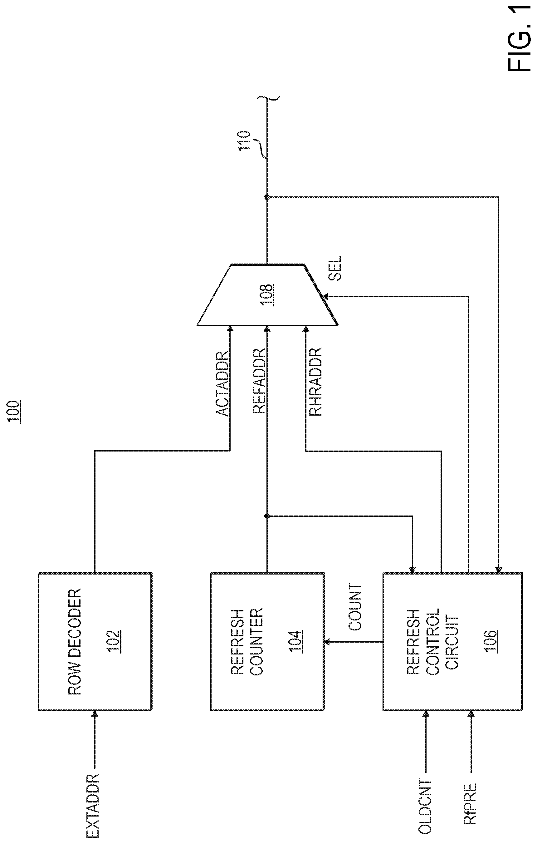
FIG. 1 is a block diagram of an apparatus according to an embodiment of the present invention.
FIG. 2 is a schematic block diagram of a refresh control circuit according to an embodiment of the present invention.
FIG. 3 is a schematic block diagram of an alternate refresh control circuit according to an embodiment of the present invention.
FIG. 4 is a block diagram of a memory including an apparatus according to an embodiment of the invention.
DETAILED DESCRIPTION
Apparatuses and methods for selective row refreshes are disclosed herein. In accordance with one or more embodiments of the described invention, one or more rows physically adjacent a target row may be refreshed. Certain details are set forth below to provide a sufficient understanding of embodiments of the invention. However, it will be clear to one having skill in the art that embodiments of the invention may be practiced without these particular details. Moreover, the particular embodiments of the present invention described herein are provided by way of example and should not be used to limit the scope of the invention to these particular embodiments. In other instances, well-known circuits, control signals, timing protocols, and software operations have not been shown in detail in order to avoid unnecessarily obscuring the invention.
Examples of the present invention relate generally to memory operations. Typically, memories, such as DRAM, operate in accordance with at least three types of operations, read operations, write operations, and refresh operations. For each operation, an active command is provided to activate (e.g., open) a particular row, a respective operation is performed on the row, and a precharge command is provided to deactivate (e.g., close) the row.
Read and write operations may be performed using an externally generated address (e.g., external address), which may be decoded into a target address. For example, the external address and an active command may be provided to a memory, and in response a target row associated with the target address may be activated. When a subsequent read or write command is provided to the memory, the memory may read data from or write data to the target row accordingly. The target row may remain activated until a precharge command is received, whereupon the target row may be deactivated.
Refresh operations may be performed using an internally generated address (e.g., refresh address). For example, a refresh command may be provided to a memory and cause a row associated with a refresh address to be refreshed. When a subsequent refresh command is provided to the memory, a row associated with a new refresh address is refreshed. In many instances, a refresh address may be provided (e.g., generated) using a counter, and the counter may increment after each refresh operation such that rows may be refreshed sequentially. Moreover, rows of memory may be refreshed in several ways. Refresh operations may, for instance, be interleaved with other operations (e.g., read operations, write operations), allowing a memory to refresh rows as necessary, while prioritizing other operations. Typically, refresh operations are performed in bursts. For example, a plurality of refresh operations may be performed in succession between operations. Accordingly, in between various read and write operations, a memory may receive a plurality of successive refresh commands, with each refresh command causing a respective row to be refreshed.
FIG. 1 is a block diagram of an apparatus 100 according to an embodiment of the invention. The apparatus 100 may include a row decoder 102, a refresh counter 104, a refresh control circuit 106, a multiplexer 108, and an address bus 110.
The row decoder 102 may be coupled to the multiplexer 108 and configured to provide a target address ACTADDR to an input of the multiplexer 108, for instance, in response to decoding an external address EXTADDR. The external address EXTADDR may comprise an externally generated address and may be provided from an external device such as controller (e.g., memory controller). The row associated with the target address ACTADDR may comprise a target row.
The refresh counter 104 may be coupled to the multiplexer 108 and configured to provide a refresh address REFADDR to an input of the multiplexer 108. In at least one embodiment, the refresh address REFADDR may be used to refresh a row associated with the refresh row address REFADDR in association with (e.g., before, prior to, during, after, in response to) a refresh operation. The refresh counter 104 may comprise a counter, such as a binary counter, and the refresh address REFADDR may comprise a count of the refresh counter 104. The refresh counter 104 may be configured to increment based, at least in part, on the control signal COUNT. In some examples, the refresh counter 104 may be configured to increment responsive, at least in part, to an edge (e.g., rising edge) of the control signal COUNT.
The refresh control circuit 106 may be coupled to the address bus 110 and configured to provide a proximate address RHRADDR to an input of the multiplexer 108. The proximate address RHRADDR may be based, at least in part, on an address, such as a target address ACTADDR provided by the multiplexer 108 via the address bus 110. In some examples, the refresh control circuit 106 may be configured to latch (e.g., store) the target address ACTADDR, for instance, in response to an active command associated with a read or write operation.
The refresh control circuit 106 may further be configured to provide the control signal SEL to the multiplexer 108. Based, at least in part, on the control signal SEL, the multiplexer 108 may selectively provide the target address ACTADDR received from the row decoder 102, the refresh address REFADDR received from the refresh counter 104, or the proximate address RHRADDR received from the refresh control circuit 106, to the address bus 110. By way of example, the refresh control circuit 106 may be configured to cause the multiplexer 108 to selectively provide the target address ACTADDR in association with read and write operations and to selectively provide the refresh address REFADDR in association with refresh operations. Accordingly, for a read operation or a write operation, data may be read from or written to a target row associated with the target address ACTADDR. For a refresh operation, a row associated with the refresh address REFADDR may be refreshed.
As will be described in more detail below, the refresh control circuit 106 may further be configured to cause the multiplexer 108 to selectively provide proximate addresses RHRADDR to the address bus 110 in association with respective interrupt operations. In some examples, providing proximate addresses RHRADDR in this manner may cause rows associated with the proximate addresses RHRADDR to be refreshed. In at least one embodiment, a proximate address RHRADDR may comprise an address associated with a row physically adjacent a target row, e.g., a row associated with a target address ACTADDR. In some examples, the refresh control circuit 106 may perform one or more interrupt operations after a particular number of refresh operations have been performed.
The refresh control circuit 106 may further be configured to receive a control signal OLDCNT. The control signal OLDCNT may be asserted, for instance by control logic (not shown in FIG. 1), each time a row is refreshed. For example, the control signal OLDCNT may be asserted when a refresh command is provided. Based, at least in part, on the control signal OLDCNT, the refresh control circuit 106 may selectively assert the control signal COUNT. As described, asserting the control signal COUNT may cause the refresh address REFADDR to be incremented. The refresh control circuit 106 may further be configured to receive a control signal RfPRE. The control signal RfPRE may be asserted, for instance by control logic (not shown in FIG. 1), each time a row is refreshed. For example, the control signal RfPRE may be asserted each time a row is precharged in association with a refresh operation.
In an example read operation or write operation of the apparatus 100, an active command and an external address EXTADDR may be provided. The row decoder 102 may decode the external address EXTADDR to provide a target address ACTADDR to the multiplexer 108, and the multiplexer 108 may selectively provide the target address ACTADDR to the address bus 110 based, at least in part, on the control signal SEL. A read or write operation may be performed, and data may be read from or written to the target row associated with the target address ACTADDR, respectively. The target row may subsequently be deactivated. The refresh control circuit 106 may receive and latch the target address ACTADDR for instance, responsive to the active command associated with the read operation or write operation.
Responsive, at least in part, to latching the output address ACTADDR, the refresh control circuit 106 may provide (e.g., generate) proximate addresses RHRADDR. As described, a proximate address RHRADDR may comprise an address associated with a row physically adjacent a target row. Thus providing proximate addresses RHRADDR may include providing addresses of rows physically adjacent the target row. By way of example, the refresh control circuit 106 may increment the target address ACTADDR to provide a first proximate address RHRADDR, and may decrement the target address ACTADDR to provide a second proximate address RHRADDR. In another example, the refresh control circuit 106 may increment or decrement the target address ACTADDR to provide a first proximate address RHRADDR. An exclusive OR (XOR) operation may be performed on the first proximate address RHRADDR and the target address ACTADDR to provide a second proximate address RHRADDR. The proximate row addresses RHRADDR may be provided after the target address ACTADDR has been latched, such as prior to and/or in association with an interrupt operation.
In an example refresh operation, a refresh command may be provided and the refresh control circuit 106 may cause the multiplexer 108 to selectively provide the refresh address REFADDR to the address bus HO. The row associated with the refresh address REFADDR may be refreshed, and the refresh address REFADDR may be incremented. As described, refresh operations may be performed in succession between other operations, such as read and write operations. Accordingly, subsequent refresh operations may be performed in response to respective refresh commands such that rows are refreshed sequentially.
After a particular number of rows have been refreshed, that is, after a particular number of refresh operations have been performed, the refresh control circuit 106 may perform an interrupt operation to refresh memory associated with a proximate address RHRADDR. Briefly, in association with an interrupt operation, a row associated with the proximate address RHRADDR may be refreshed. The refresh control circuit 106 may determine the number of rows refreshed based, at least in part, on the refresh address REFADDR, for instance, by determining that a particular bit of the refresh address REFADDR has transitioned from a first state to a second state (e.g., logic low to logic high). For example, a transition of a ninth least significant bit of a refresh address REFADDR that was incremented by one starting from zero may indicate that 256 rows have been refreshed.
Performing an interrupt operation may include the multiplexer 108 selectively providing a proximate address RHRADDR to the address bus 110. This may in turn cause the row associated with the proximate address RHRADDR to be refreshed. In one embodiment, interrupt operations may be performed consecutively until rows associated with a plurality of proximate addresses RHRADDR have been refreshed. In other embodiments, interrupt operations are not performed consecutively.
In at least one embodiment, the refresh control circuit 106 may be configured to perform an interrupt operation responsive, at least in part, to a refresh command. For example, once the refresh control circuit 106 has determined that a particular number of rows have been refreshed, the refresh control circuit 106 may perform an interrupt operation in response to a subsequent refresh command, or in response to each of a plurality of subsequent refresh commands for a plurality of proximate addresses RHRADDR. In response to each refresh command, the refresh control circuit 106 may provide a proximate address RHRADDR such that the row associated with the respective proximate address RHRADDR is refreshed.
In association with interrupt operations, the refresh control circuit 106 may not assert the control signal COUNT. In this manner, the refresh control circuit 106 may hold the refresh address REFADDR at a same value while a row associated with the proximate address RHRADDR is refreshed in association with the interrupt operation. Thus, after interrupt operations have completed, the refresh control circuit 106 may assert the control signal COUNT responsive to a subsequent refresh command so that the refresh counter 104 may resume providing addresses without "skipping" a refresh of a row as a result of an interrupt operation during which a row associated with a proximate address RHRADDR is refreshed.
As described, the refresh control circuit 106 may be configured to latch a target address ACTADDR. In at least one embodiment, the refresh control circuit 106 may be configured to latch the most recent target address ACTADDR such that the most recent address provided by the row decoder 102 is used to provide a proximate address RHRADDR, and therefore the row or rows refreshed in association with interrupt operations. In other embodiments, the refresh control circuit 106 may be configured to latch multiple target addresses ACTADDR. For example, the refresh control circuit 106 may be configured to latch (e.g., store) the previous four target addresses ACTADDR provided by the row decoder 102. Accordingly, interrupt operations may include refreshing rows physically adjacent one or more of the latched target addresses ACTADDR.
In some embodiments, the refresh control circuit 106 may further be configured to selectively perform refresh operations. For example, the refresh control circuit 106 may be configured to perform an interrupt operation to refresh a row if the row is functional. In this manner, accessing malfunctioning and/or damaged rows may be avoided. Moreover, if the target row is a boundary row (e.g., a row of primary memory physically adjacent a redundant portion or a row of redundant memory physically adjacent a primary portion), the refresh control circuit 106 may be configured to selectively perform an interrupt operation to refresh an adjacent row in a neighboring portion if the adjacent row is functional.
As described, if a target row is repeatedly accessed (e.g., in association with a read operation or a write operation), coupling effects may result in increased cell to cell leakage, and degradation of data stored in rows physically adjacent a repetitively accessed row. Accordingly, by refreshing rows associated with proximate addresses RHRADDR in association with refresh operations, the physically adjacent rows may be refreshed more frequently, thereby reducing degradation of the data stored by the adjacent rows. By latching the most recent target address, and subsequently refreshing the rows physically adjacent the target row associated with the target address, the physically adjacent rows may be refreshed without a need to determine a number of times a row is accessed within a particular period of time.
FIG. 2 is a schematic block diagram of a refresh control circuit 200 according to an embodiment of the present invention. The refresh control circuit 200 may be used to implement the refresh control circuit 106 of FIG. 1. The refresh control circuit 200 may include an address control circuit 202, an alternate refresh control circuit 204, and an AND logic gate 206.
The address control circuit 202 may be configured to receive the target address ACTADDR and provide the proximate address RHRADDR. As described, the address control circuit 202 may provide one or more proximate addresses RHRADDR based, at least in part, on the target address ACTADDR. A proximate row addresses RHRADDR may be associated with a row physically adjacent a target row.
The alternate refresh control circuit 204 may be configured to receive the refresh row address REFADDR, for instance, from the refresh counter 104 of FIG. 1, and further may receive the control signal RfPRE. Based, at least in part, on the refresh row address REFADDR and the control signal RfPRE, the alternate refresh control circuit 204 may provide a control signal RHRfshF. The alternate refresh control circuit 204 may, for instance, assert the control signal RHRfshF in association with read and write operations and refresh operations.
The AND logic gate 206 may receive the control signal RHRfshF and the control signal OLDCNT. The control signal OLDCNT may be asserted in response to a row being refreshed, for instance in association with a refresh operation and/or an interrupt operation. Because the control signal RHRfshF may not be asserted during interrupt operations, however, the AND logic gate may assert the COUNT signal responsive to a row being refreshed in association with a refresh operation. In this manner, the refresh address REFADDR may be incremented responsive to refreshes associated with refresh operations, in contrast to refreshes associated with interrupt operations.
The alternate refresh control circuit 204 may further be configured to provide the control signal SEL and cause the multiplexer 108 of FIG. 1 to selectively provide the target address ACTADDR, the refresh address REFADDR, or the proximate address RHRADDR to the address bus 110 in association with read and write operations, refresh operations, and interrupt operations, respectively.
FIG. 3 is a schematic block diagram of an alternate refresh control circuit 300 according to an embodiment of the present invention. The alternate refresh control circuit 300 may be used to implement the alternate refresh control circuit 204 of FIG. 2. The alternate refresh control circuit 300 may include a pulse generator 302, flip-flops 304, 306, a set-reset (SR) latch 308, an inverter 310, and selection logic 312.
The pulse generator 302 may be configured to receive the refresh address REFADDR, for instance, from the refresh counter 104 of FIG. 1. Based, at least in part, on the refresh address REFADDR, the pulse generator 302 may provide a pulse to the SR latch 308. In some examples, the pulse generator 302 may be configured to provide a pulse responsive to determining that a particular number of refresh operations have been performed. This may, for instance, include determining that a particular hit of the refresh address REFADDR has transitioned from a first state to a second state. The flip-flops 304, 306 may be configured to receive the control signals RHRfshF and RfPRE at reset R and clock CLK inputs, respectively. The flip-flop 304 may be configured to receive a logic high supply voltage at its data S input.
The SR latch 308 may be configured to receive pulses from the pulse generator at a first S input and to receive the output of the flip-flop 306 at a second R input. The SR latch 308 may be configured to provide a control signal RHRfsh. The control signal RHRfsh may be received by the inverter 310 and inverted to provide the control signal RHRfshF.
The selection logic 312 may be configured to receive the control signal RHRfsh and provide the control signal SEL. As previously described, the control signal SEL may be provided to the multiplexer 108 of FIG. 1 to cause the multiplexer 108 to selectively provide the target address ACTADDR, the refresh address REFADDR, or the proximate address RHRADDR to an address bus, such as the address bus 110 of FIG. 1. The selection logic 312 may be configured to cause the multiplexer 108 to provide proximate addresses RHRADDR responsive the control signal RHRfsh being asserted.
In an example operation, the pulse generator 302 may determine that a particular number of refresh operations have been performed, for example, that a particular bit of the refresh address REFADDR has transitioned between states. As a result, the pulse generator 302 may provide a pulse to the SR latch 308.
In response, the SR latch 308 may provide an asserted control signal RHRfsh and the selection logic 312 may in turn cause the multiplexer 108 to provide a first proximate address RHRADDR to the address bus 110 in association with a first interrupt operation. As a result, a row associated with the proximate row address RHRADDR may be refreshed. Concurrently, the inverter 310 may invert the asserted control signal RHRfsh to provide the control signal RHRfshF. The control signal RHRfshF may not be asserted and thereby not cause the flip-flops 304, 306 to reset.
After the row associated with the first proximate row address RHRADDR is refreshed, the control signal RfPRE may be asserted and cause the flip-flops 304, 306 to clock such that the output of the flip-flop 304 transitions to a logic high level. A second proximate row address RHRADDR may be provided in association with a second interrupt operation and a row associated with the second proximate row address RHRADDR may be refreshed. After the row is refreshed, the control signal RfPRE may once again be asserted and cause the flip-flops 304, 306 to clock such that the output of the flip-flop 306 transitions to a logic high level. This may in turn cause the SR latch 308 to reset and cease asserting the control signal RHRfsh. The flip-flops 304, 306 may return to the reset state responsive to the control signal RHRfshF, and the selection logic 312 may cause the multiplexer 108 to selectively provide the refresh row address REFADDR to the address bus 110 such that refresh operations may resume. The first and second proximate row addresses RHRADDR may be associated with two rows adjacent a latched target row address. Refreshing the two adjacent rows in association with the first and second interrupt operations may prevent data stored by memory cells of the two adjacent rows from being degraded by repeated accesses of the row associated with the latched target row address.
In some examples, refreshing a row may include refreshing a plurality of memory cells. Moreover, a plurality of memory cells may comprise either a row of memory cells and/or a column of memory cells. Accordingly, although examples described herein are directed to selective row refreshes, it will be appreciated that described examples may be applied to memory cells such that selective column refreshes may be performed as well. In this manner, embodiments described herein may be applied to refresh a plurality of memory cells configured in any arrangement, such as in a row, column, fat row (e.g., multiple rows), fat column (multiple columns), or combination thereof.
FIG. 4 is a block diagram of a memory 400 including an apparatus according to an embodiment of the invention. The memory 400 includes an array 402 of memory cells, which may be, for example, volatile memory cells, non-volatile memory cells, DRAM memory cells, SRAM memory cells, flash memory cells, or other types of memory cells. The memory 400 includes a command decoder 406 that receives memory commands and addresses through an ADDR/CMD bus. The command decoder 404 provides control signals, based on the commands received through the command bus 405. The command decoder 404 also provides row and column addresses to the memory 400 through an address bus 425 and an address latch 406. The address latch then outputs separate column addresses and separate row addresses.
The row and column addresses are provided by the address latch 406 to a row decoder 410 and a column decoder 408, respectively. The row decoder may comprise a row decoder described herein, such as the row decoder 102 of FIG. 1. The column decoder 408 selects bit lines extending through the array 402 corresponding to respective column addresses. The row decoder 410 is coupled to a multiplexer 444, which may comprise any multiplexer described herein, such as the multiplexer 108 of FIG. 1. A refresh counter 440 and a refresh control circuit 442 according to an embodiment of the invention may further be coupled to the multiplexer 444. For example, the refresh counter 440 and the refresh control circuit 442 may comprise a refresh counter and refresh control circuit described herein. The multiplexer 444 may be coupled to word line driver 424 that activates respective rows of memory cells in the array 402 corresponding to received row addresses. The selected data line (e.g., a bit line or bit lines) corresponding to a received column address is coupled to a read/write circuitry 414 to provide read data to a data output circuit 416 via an input-output data bus 415. Write data are provided to the array 402 through a data input circuit 418 and the memory array read/write circuitry 414. The command decoder 404 responds to memory commands and addresses provided to the command bus to perform various operations on the array 402. In particular, the command decoder 404 is used to provide control signals to read data from and write data to the array 402.
From the foregoing it will be appreciated that, although specific embodiments of the invention have been described herein for purposes of illustration, various modifications may be made without deviating from the spirit and scope of the invention. Accordingly, the invention is not limited except as by the appended claims.
* * * * *
D00000
D00001
D00002
D00003
D00004
XML
uspto.report is an independent third-party trademark research tool that is not affiliated, endorsed, or sponsored by the United States Patent and Trademark Office (USPTO) or any other governmental organization. The information provided by uspto.report is based on publicly available data at the time of writing and is intended for informational purposes only.
While we strive to provide accurate and up-to-date information, we do not guarantee the accuracy, completeness, reliability, or suitability of the information displayed on this site. The use of this site is at your own risk. Any reliance you place on such information is therefore strictly at your own risk.
All official trademark data, including owner information, should be verified by visiting the official USPTO website at www.uspto.gov. This site is not intended to replace professional legal advice and should not be used as a substitute for consulting with a legal professional who is knowledgeable about trademark law.