Flow-regulated growth of nanotubes
Wan , et al. February 2, 2
U.S. patent number 10,907,265 [Application Number 15/669,034] was granted by the patent office on 2021-02-02 for flow-regulated growth of nanotubes. This patent grant is currently assigned to Rochester Institute of Technology. The grantee listed for this patent is Rong Fan, Jiandi Wan, Zihao Wang. Invention is credited to Rong Fan, Jiandi Wan, Zihao Wang.


View All Diagrams
| United States Patent | 10,907,265 |
| Wan , et al. | February 2, 2021 |
Flow-regulated growth of nanotubes
Abstract
A method for growing nanotubes via flow-regulated microfluidic electrochemical anodization, includes providing a microfluidic device having a fluid inlet; a fluid outlet; and a fluidic microchannel connecting the fluid inlet and outlet, wherein the microchannel includes a Pt cathode and a Ti anode separated by an electrical insulator; providing an electrolyte fluid flow through the microchannel; and providing an electrical current across the anode and cathode sufficient to cause electrochemical anodization growth of TiO.sub.2 nanotubes in the microchannel on a surface of the anode.
| Inventors: | Wan; Jiandi (Pittsford, NY), Fan; Rong (Rochester, NY), Wang; Zihao (Rochester, NY) | ||||||||||
|---|---|---|---|---|---|---|---|---|---|---|---|
| Applicant: |
|
||||||||||
| Assignee: | Rochester Institute of
Technology (Rochester, NY) |
||||||||||
| Family ID: | 1000005335129 | ||||||||||
| Appl. No.: | 15/669,034 | ||||||||||
| Filed: | August 4, 2017 |
Prior Publication Data
| Document Identifier | Publication Date | |
|---|---|---|
| US 20180038006 A1 | Feb 8, 2018 | |
Related U.S. Patent Documents
| Application Number | Filing Date | Patent Number | Issue Date | ||
|---|---|---|---|---|---|
| 62435929 | Dec 19, 2016 | ||||
| 62371033 | Aug 4, 2016 | ||||
| Current U.S. Class: | 1/1 |
| Current CPC Class: | C25D 11/26 (20130101); C25D 11/04 (20130101); C25D 1/006 (20130101) |
| Current International Class: | C25D 11/26 (20060101); C25D 1/00 (20060101); C25D 11/04 (20060101) |
References Cited [Referenced By]
U.S. Patent Documents
| 5700366 | December 1997 | Steblianko |
| 2003/0059992 | March 2003 | Cotte |
Other References
|
Bhattacharya J., et al., "Microfluidic anodization of aluminum films for the fabrication of nanoporous lipid bilayer support structures", Beilstein Journal of Nanotechnology, 2011, 2, 104-109. (Year: 2011). cited by examiner . Aerts, T., et al., "Experimental study and modeling of heat transfer during anodizing in a wall-jet set-up", Simulation of Electrochemical Processes II, vol. 54, 193-202, 2007. (Year: 2007). cited by examiner . Krivec, M., et al., "Highly Efficient TiO2-based microreactor for photocatalytic applications", ACS Applied Materials & Interfaces, 2013, 5, 9088-9094. (Year: 2013). cited by examiner . Raoufi, M., et al., "Improved synthesis of anodized aluminum oxide with modulated pore diameters for the fabrication of polymeric nanotubes", RSC Advances, 2013, 3, 13429-13436. (Year: 2013). cited by examiner . Lamberti et al. "Microfluidic electrochemical growth of vertically aligned TiO2 nanotubes for SERS optofluidic devices", RSC Advances, 2015, 5, 105484-105488 (Year: 2015). cited by examiner. |
Primary Examiner: Wittenberg; Stefanie S
Attorney, Agent or Firm: Bond, Schoeneck & King, PLLC Noto; Joseph
Government Interests
STATEMENT REGARDING FEDERALLY SPONSORED RESEARCH FOR DEVELOPMENT
This invention was made with Government support under Agency Grant No. 56679 awarded by NYSERDA. The government has certain rights in the invention.
Parent Case Text
RELATED APPLICATION DATA
This application claims the benefit of priority of U.S. Provisional Patent Application No. 62/435,929 filed on Dec. 19, 2016 and U.S. Provisional Patent Application No. 62/371,033 filed on Aug. 4, 2016, the subject matter of all being incorporated herein by reference in their entireties.
Claims
What is claimed:
1. A method for growing nanotubes via flow-regulated electrochemical anodization, comprising: flowing in a laminar flow an electrolyte between a metal anode and metal cathode within a channel up to 500 microns wide, wherein the distance between the anode and cathode is from 150 microns to 2050 microns; providing an electrical current across the anode and cathode sufficient to cause electrochemical anodization growth of nanotubes on a surface of the anode; and controlling a rate of the laminar flow to effect a desired growth of the nanotubes in a laminar flow region, wherein the laminar flow comprises a flow rate having a Peclet number of above 100 sufficient to inhibit growth of an oxide layer on the nanotubes.
2. The method of claim 1, wherein the flow is a microfluidic flow.
3. The method of claim 1, wherein the metal cathode comprises Pt.
4. The method of claim 1, wherein the metal anode comprises titanium, aluminum, vanadium, zirconium, hafnium, niobium, tantalum, or tungsten.
5. The method of claim 1, wherein the nanotubes comprise TiO.sub.2.
6. The method of claim 1, wherein the flow rate is controlled to determine the length of the nanotubes.
7. The method of claim 1, wherein the flow rate is controlled to determine the inner and outer diameter of the nanotubes.
8. The method of claim 1, wherein the laminar flow comprises a flow profile which is controlled to determine the distribution of the nanotubes within the channel.
9. The method of claim 1, wherein the laminar flow comprises a Reynolds number of below about 2000.
10. The method of claim 1, wherein the flow rate comprises a Peclet number of above about 1000.
Description
FIELD
This disclosure relates to flow-regulated growth of nanotubes, and in particular, to methods and devices for flow-regulated growth of nanotubes via electrochemical anodization.
BACKGROUND
Due to the inherent material properties of TiO.sub.2 and unique features of nanotubes, TiO.sub.2 nanotubes find a wide range of applications including but not limited to photo-catalysis, solar cells, electrochromic devices, sensors, bio-coating, and drug delivery. Although many approaches such as sol-gel, electrochemical lithography, and hydrothermal synthesis have been developed to produce TiO.sub.2 nanotubes, anodic growth of TiO.sub.2 nanotubes is one of the most common methods to produce highly ordered nanotube arrays. TiO.sub.2 nanotubes are commonly grown using electrochemical anodization, in which a complex field-aided oxidation and dissolution process is responsible for the formation of TiO.sub.2 nanotubes. During anodization, titanium metal is oxidized to a TiO.sub.2 layer on the top of the metal surface, which is subsequently dissolved via a field-assisted electrochemical process to produce the TiO.sub.2 nanotubes. The continuous competition of the field-assisted oxidation and dissolution is believed to control the growth of TiO.sub.2 nanotube arrays.
To date, all the approaches used to grow TiO.sub.2 nanotubes are conducted in bulk conditions, e.g., with a relatively large distance (>5 cm) between the anode and cathode. In these cases, it takes long time (tens of hours) to grow long (in the ranges of micrometers) nanotubes and there is always an oxide layer on top of the synthesized nanotubes, compromising the applications of such TiO.sub.2 nanotubes. To date, most approaches to electrochemically produce TiO.sub.2 nanotubes are conducted under static, bulk conditions during anodization. In this case, an initially formed, compact oxide layer with random pores often remains on the top of the TiO.sub.2 nanotube arrays after anodization. The existence of the compact oxide layer significantly limits the growth and application of TiO.sub.2 nanotubes. In addition, extended anodization time, which is required to produce long TiO.sub.2 nanotubes (e.g., high aspect ratios), frequently leads to inhomogeneous tube diameter and structure due to the F-based chemical etching process. Introducing hydrodynamic factors such as stirring to the electrolyte solution during anodization increases the length of TiO.sub.2 nanotubes up to 60%, the flow, however, is not well-controlled and the morphological homogeneity of nanotubes is negatively affected.
In addition, although stirring the electrolyte solution during anodization has shown to be able to increase the length of TiO.sub.2 nanotubes, the solution flow is not well controlled and the morphological homogeneity of the TiO.sub.2 nanotubes is negatively affected. As a result, stagnant solutions are preferred for the growth of uniform layers.
Thus, the art lacks a method in which the rate of anodic growth of TiO.sub.2 nanotubes is significantly enhanced. A method which controls the diameter, length, and crystal orientations of TiO.sub.2 nanotubes and determines the spatial distribution of nanotubes is also desired. Further lacking is a method in which both vertically and horizontally aligned TiO.sub.2 nanotubes can be produced. The present invention provides regulation of the growth of TiO.sub.2 nanotubes and effective strategies to enhance the production of TiO.sub.2 nanotubes with controlled orientation and structural properties in a manner not suggested or contemplated by the art.
SUMMARY
In accordance with an aspect of the present invention, there is provided a method for growing nanotubes via flow-regulated electrochemical anodization, including flowing in a laminar flow an electrolyte between a metal anode and metal cathode; and providing an electrical current across the anode and cathode sufficient to cause electrochemical anodization growth of nanotubes on a surface of the anode, wherein the laminar flow has a flow rate sufficient to inhibit growth of an oxide layer on the nanotubes.
In accordance with another aspect of the present invention, there is provided a device for growing nanotubes via flow-regulated electrochemical anodization, including: a fluid inlet; a fluid outlet; and a channel connecting the fluid inlet and fluid outlet, wherein the channel includes a metal cathode and a metal anode separated by an electrical insulator, wherein the channel is capable of receiving a laminar flow of electrolytic fluid at a flow rate sufficient to cause electrochemical anodization growth of nanotubes on a surface of the anode and inhibit growth of an oxide layer on the nanotubes when an electrical current is placed across the anode and cathode.
BRIEF DESCRIPTION OF THE DRAWINGS
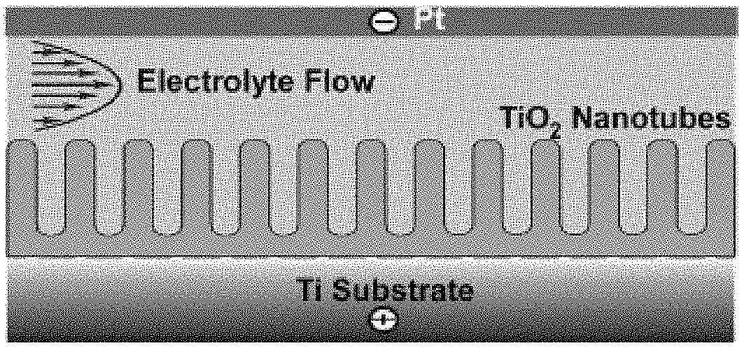
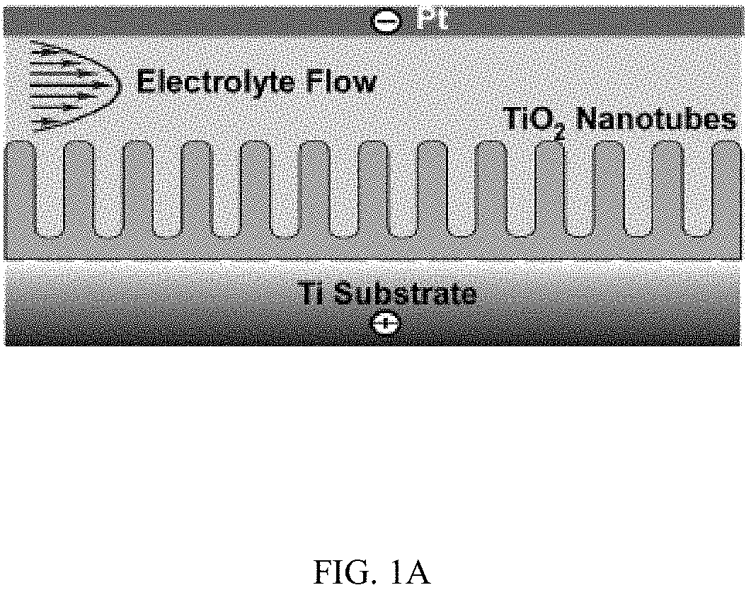
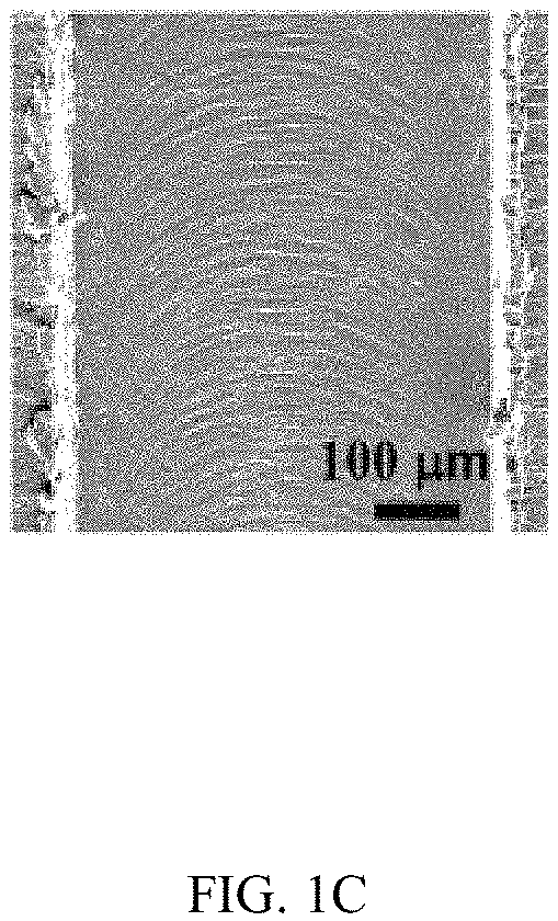
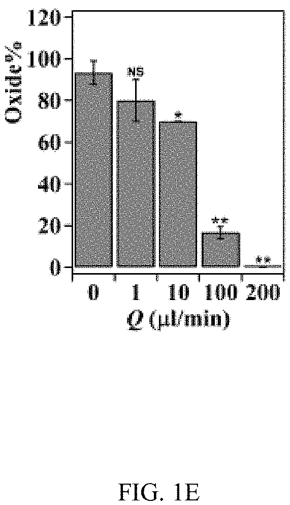
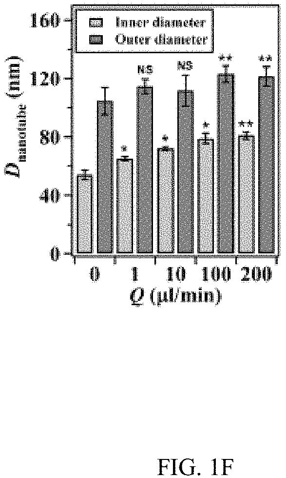
FIGS. 1A-1M illustrates the effect of flow on the growth of TiO.sub.2 nanotubes in microfluidics, FIG. 1A is a schematic, FIG. 1B is an image of an embodiment of an assembled microfluidic device, FIG. 1C is an SEM image, FIG. 1D is a graph, FIG. 1E is a graph, FIG. 1F is a graph, FIG. 1G is a graph, FIGS. 1H & 1I are SEM images, FIGS. 1J & 1K are SEM images, FIG. 1L shows XRD patterns, and FIG. 1M is a graph;
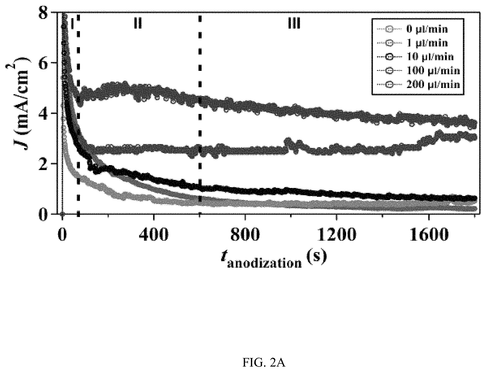
FIGS. 2A-2D illustrates the effect of flow on the current density during anodization, FIG. 2A shows current-time curves, FIG. 2B is a graph, FIG. 2C is a graph, and FIG. 2D illustrates a schematic;
FIGS. 3A-3J illustrates the effect of flow on the spatial growth of TiO.sub.2 nanotubes in microfluidics, FIG. 3A is a schematic, FIG. 3B is a graph, FIG. 3C is a graph, FIG. 3D is a series of SEM images, FIG. 3E is a series of SEM images, FIG. 3F is a schematic, FIG. 3G is a graph, FIG. 3H is a graph, FIG. 3I is a series of SEM images, and FIG. 3J is a series of SEM images;
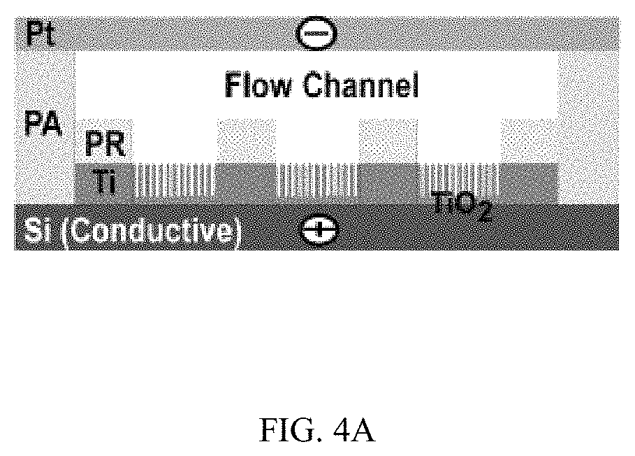
FIGS. 4A-4H illustrates control of the growth of TiO.sub.2 nanotubes on silicon substrates, FIG. 4A is a schematic, FIG. 4B is a series of SEM images, FIG. 4C are high resolution SEM images, FIG. 4D is a schematic, FIG. 4E is an SEM image, FIGS. 4F & 4G are graphs, and FIG. 4H is a schematic;
FIGS. 5A-5C show the characterization of TiO.sub.2 nanotubes using energy dispersive X-ray spectroscopy (EDS), FIG. 5A is an SEM image, FIG. 5B is an SEM image, and FIG. 5C is a graph;
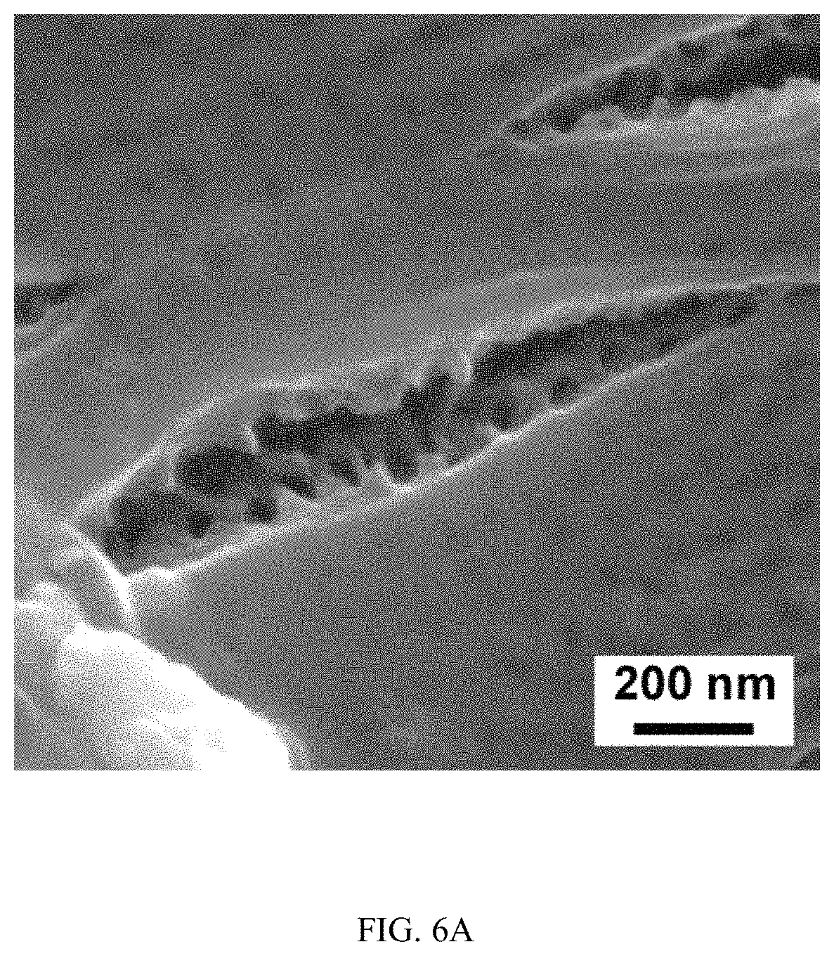
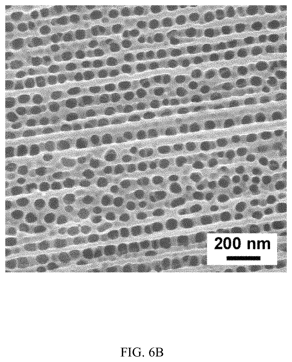
FIGS. 6A-6B show the effect of flow on the growth of the oxide layer formed at the oxide-electrolyte interface, FIGS. 6A & 6B are SEM images;
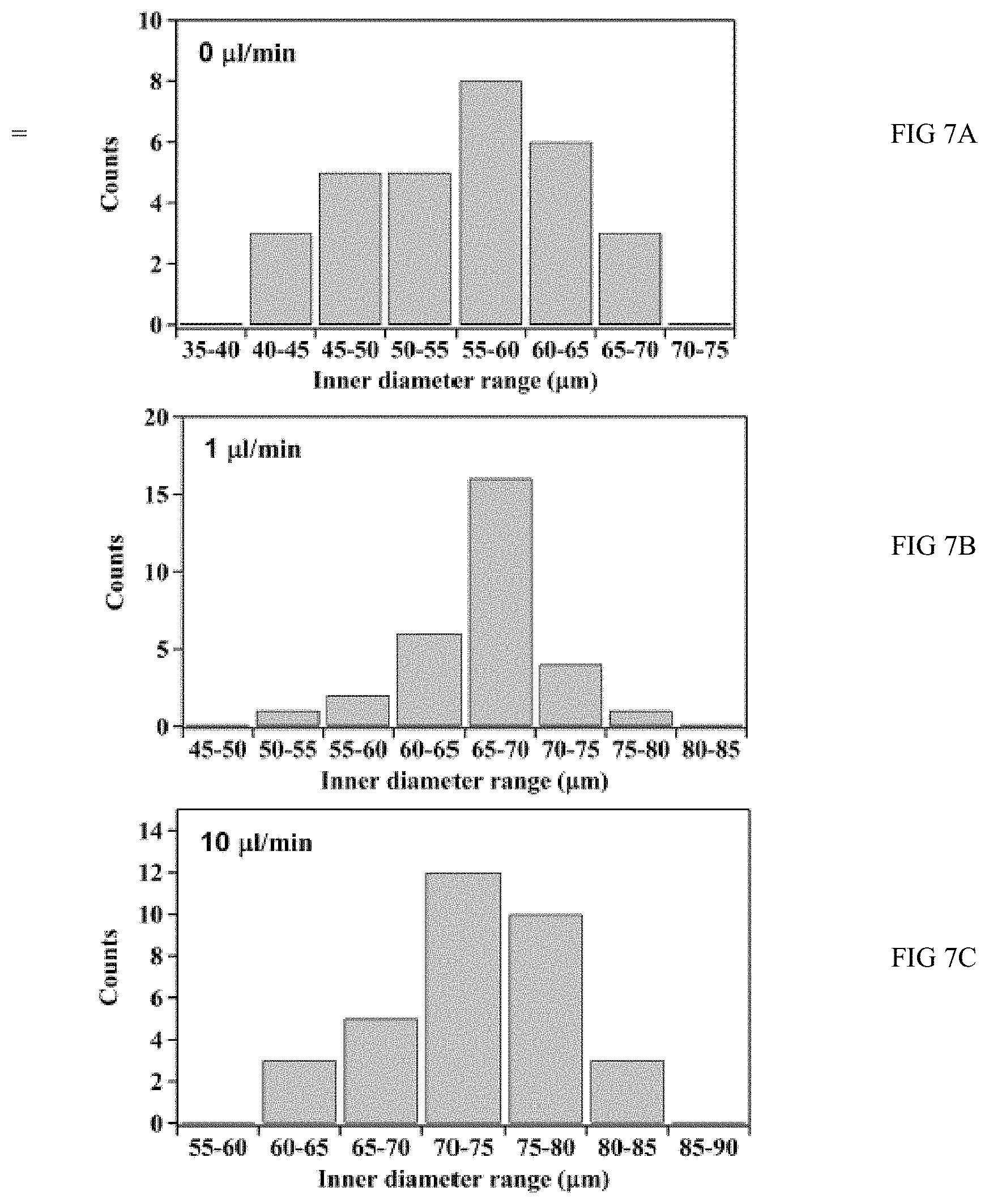
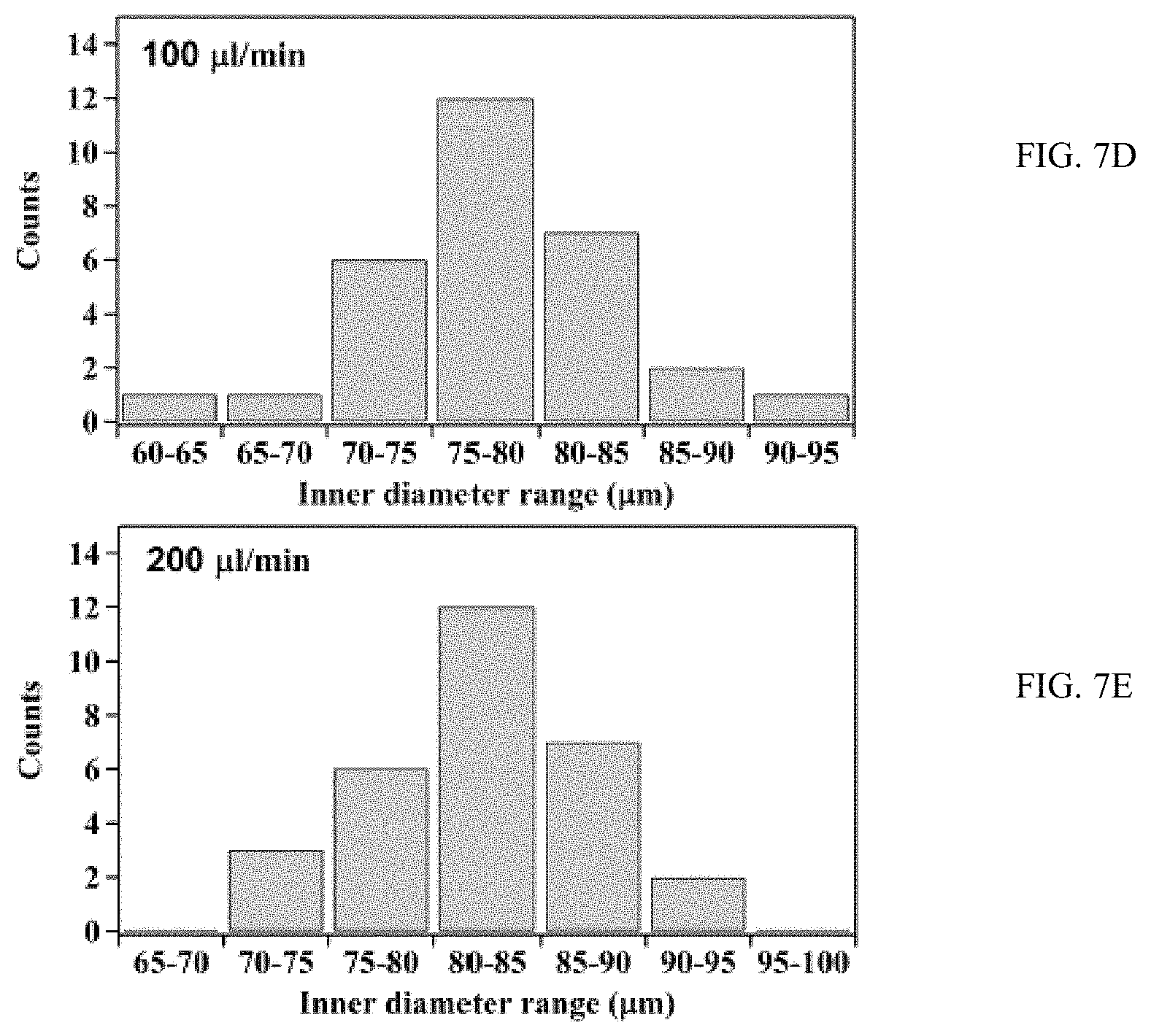
FIGS. 7A, 7B, 7C, 7D, and 7E are graphs of flow rate verses inner diameter;
FIGS. 8A-8C shows the effect of flow on the spatial growth of TiO.sub.2 nanotubes in microfluidics at different locations along the microfluidic channel, FIG. 8A is a schematic, FIG. 8B and FIG. 8C are plots;
FIGS. 9A-9C shows the effect of flow on the spatial growth of TiO.sub.2 nanotubes in microfluidics at different locations along the microfluidic channel, FIG. 9A is a schematic, FIG. 9B and FIG. 9C are plots;
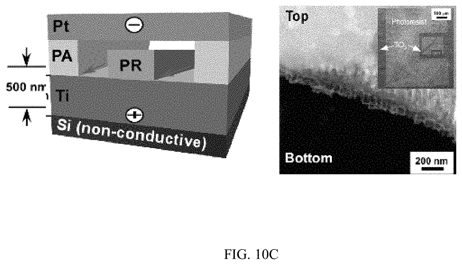
FIGS. 10A-10C shows the horizontal growth of TiO.sub.2 nanotubes on non-conductive silicon substrates, FIG. 10A shows a schematic and SEM image, FIG. 10B shows a schematic and SEM image, and FIG. 10C shows a schematic and SEM image;
FIG. 11 is an SEM image of TiO.sub.2 nanotubes;
FIGS. 12A-12B show TiO.sub.2 nanotubes growing on a non-conductive silicon substrate, FIG. 12A is a set of SEM images and FIG. 12B is a set of SEM images;
FIG. 13 shows an SEM image;
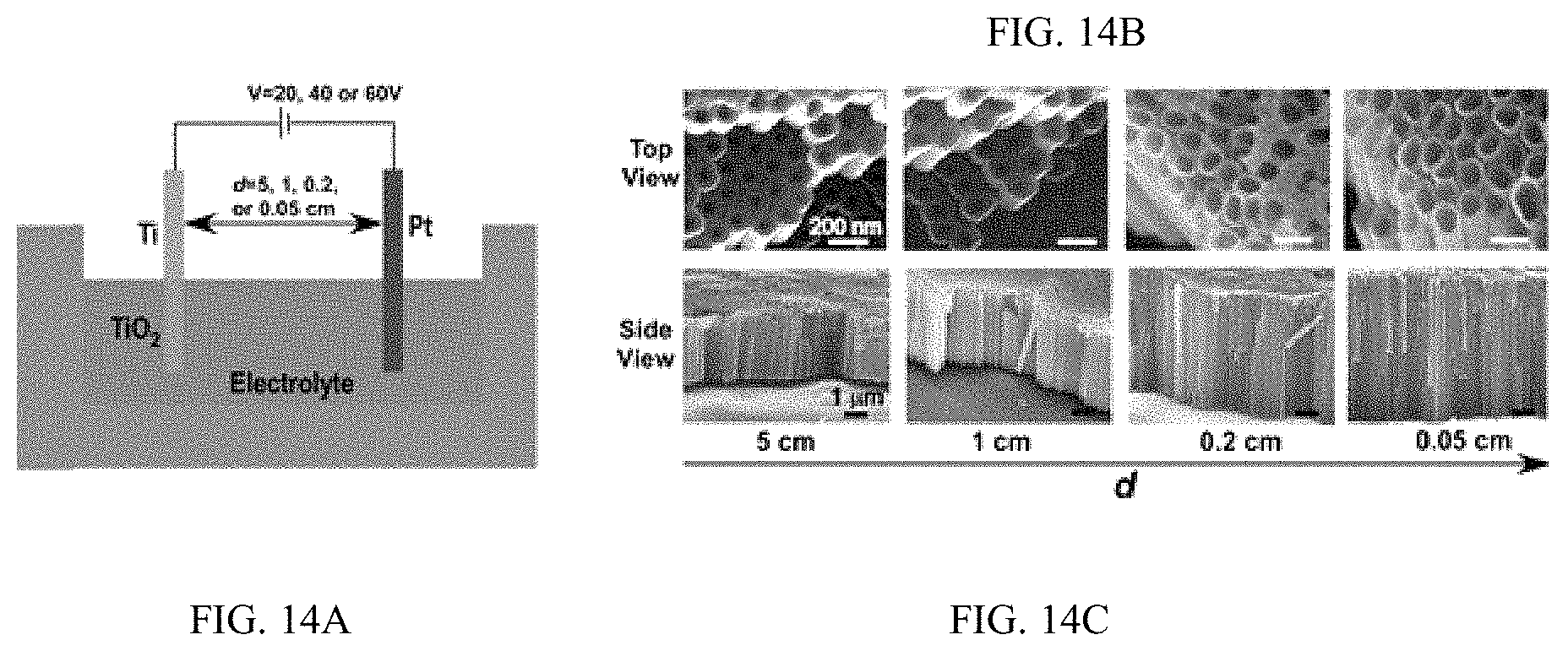
FIGS. 14A-14C illustrate electrode distance regulates the anodic growth of TiO.sub.2 nanotube, FIG. 14A shows a schematic, FIG. 14B is a series of SEM images, and FIG. 14C is a series of SEM images;
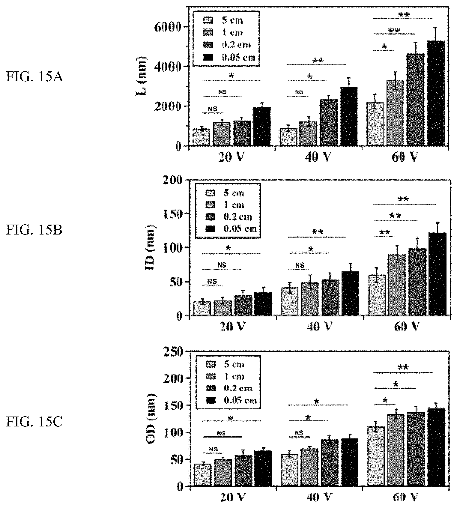
FIGS. 15A-C show the effect of electrode distance (d) on the growth of TiO.sub.2 nanotubes at different anodizing voltages, FIG. 15A is a plot, FIG. 15B is a plot, and FIG. 15C is a plot;
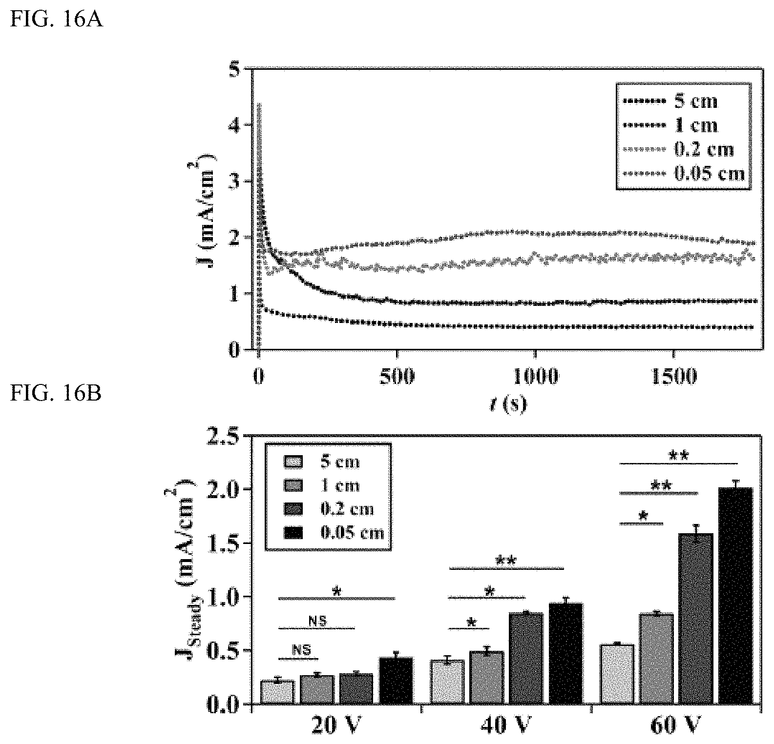
FIGS. 16A-16B show electrode distance (d) regulates current density (J) during the anodic growth of TiO.sub.2 nanotubes, FIG. 16A shows a graph and FIG. 16B shows a plot; and
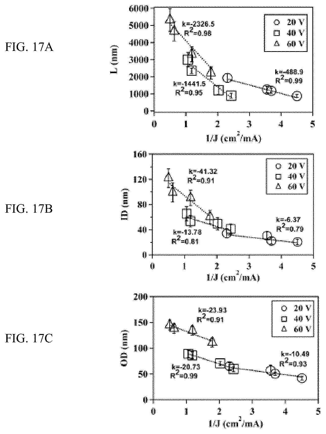
FIGS. 17A-17C shows inverse of the current density (J) correlates linearly with the structure of TiO.sub.2 nanotubes, FIG. 17A shows a plot, FIG. 17B shows a plot, and FIG. 17C shows a plot.
DETAILED DESCRIPTION
The present invention provides a method and device wherein the flow associated with the growth of nanotubes is well controlled and flow rate can be changed systematically to affect a desired outcome. Suitable control is provided by a system using laminar flow, and in particular, 2-D laminar flow of the electrolyte solution. In addition, this method and system significantly decreases production time and improves product (e.g., without forming the oxide layer). Most importantly, this invention allows for growing TiO.sub.2 nanotubes in a horizontal direction, which will open doors for the manipulation of spatial growth of nanotubes in hierarchical structures and fabrication of nano/micro devices involving horizontal TiO.sub.2 nanotubes.
A method for growing nanotubes via flow-regulated electrochemical anodization, includes flowing in a laminar flow an electrolyte between a metal anode and metal cathode; and providing an electrical current across the anode and cathode sufficient to cause electrochemical anodization growth of nanotubes on a surface of the anode, wherein the laminar flow has a flow rate sufficient to inhibit growth of an oxide layer on the nanotubes.
A device for growing nanotubes via flow-regulated electrochemical anodization, includes: a fluid inlet; a fluid outlet; and a channel connecting the fluid inlet and fluid outlet, wherein the channel includes a metal cathode and a metal anode separated by an electrical insulator, and wherein the channel is capable of receiving a laminar flow of electrolytic fluid at a flow rate sufficient to cause electrochemical anodization growth of nanotubes on a surface of the anode and inhibit growth of an oxide layer on the nanotubes when an electrical current is placed across the anode and cathode.
This invention significantly accelerates the process of TiO.sub.2 nanotubes growth and improves the quality of nanotubes by simultaneously removing the oxide layer while growing the nanotubes. Suitable electrolyte compositions include known electrolytes used for anodization.
An embodiment includes a microfluidic approach to grow, for example, TiO.sub.2 nanotubes, via electrochemical anodization. The method is not limited to the growth of TiO.sub.2 nanotubes and applies to any metals in which nanotubes can be grown via electrochemical anodization. Suitable metals include valve metals or any metals that build self-protecting oxide layers against corrosion. Suitable metals include aluminum, titanium, vanadium, zirconium, hafnium, niobium, tantalum, tungsten and others.
In an embodiment, TiO.sub.2 nanotubes with length of 4 .mu.m, outer diameter of 110-120 nm and wall thickness of 40 nm can be fabricated directly in a microfluidic channel. Comparing to the distance between anode and cathode in conventional electrochemical anodization in bulk solutions (>5 cm), the current invention has a much smaller anode-to-cathode distance (e.g., 150-2050 .mu.m), and thus provides a miniature device model to fabricate TiO.sub.2 nanotubes.
Flow in the microfluidic channel significantly reduces the thickness of the oxide layer grown at the oxide-electrolyte interface during anodization. The growth of TiO.sub.2 nanotubes was much faster in flow conditions in microfluidics than that of conventional methods. The length of TiO.sub.2 nanotubes grown can be as high as .about.4 .mu.m during 30 min anodization at 40 V. In comparison, the length of TiO.sub.2 nanotubes is 400 nm when there is no flow during the growth process in microfluidics and the length of TiO.sub.2 nanotubes obtained from conventional electrochemical anodization in bulk is 6 .mu.m for 19 hours anodization at 40 V.
The spatial distribution of the length of TiO.sub.2 nanotubes fabricated in microfluidics can be controlled by adjusting the flow profile inside the channel. A parabolic flow profile parallel to the surface of the channel produces TiO.sub.2 nanotubes with the largest length in the middle of the channel and short tubes at the edge of the channel.
TiO.sub.2 nanotubes can grow on silicon surface with patterned arbitrary shapes including but not limited to a circle, triangle, and square shapes and letters.
The utility of the present disclosure includes but is not limited to the following uses: integrate TiO.sub.2 nanotubes with silicon-based devices; integrate TiO.sub.2 nanotubes with dye-sensitized solar cells; integrate TiO.sub.2 nanotubes in flow for solar fuel production; and integrate TiO.sub.2 nanotubes in flow for water purification.
This process can be implementing to any existing process for the generation of TiO.sub.2 nanotubes. As a result, existing applications of TiO.sub.2 nanotubes will apply to this invention. In particular, this process can be used to fabricate TiO.sub.2 nanotubes on 1) silicon chips or CMOS; 2) portable or miniature devices for TiO.sub.2-based energy production; and 3) TiO.sub.2-based water purification devices.
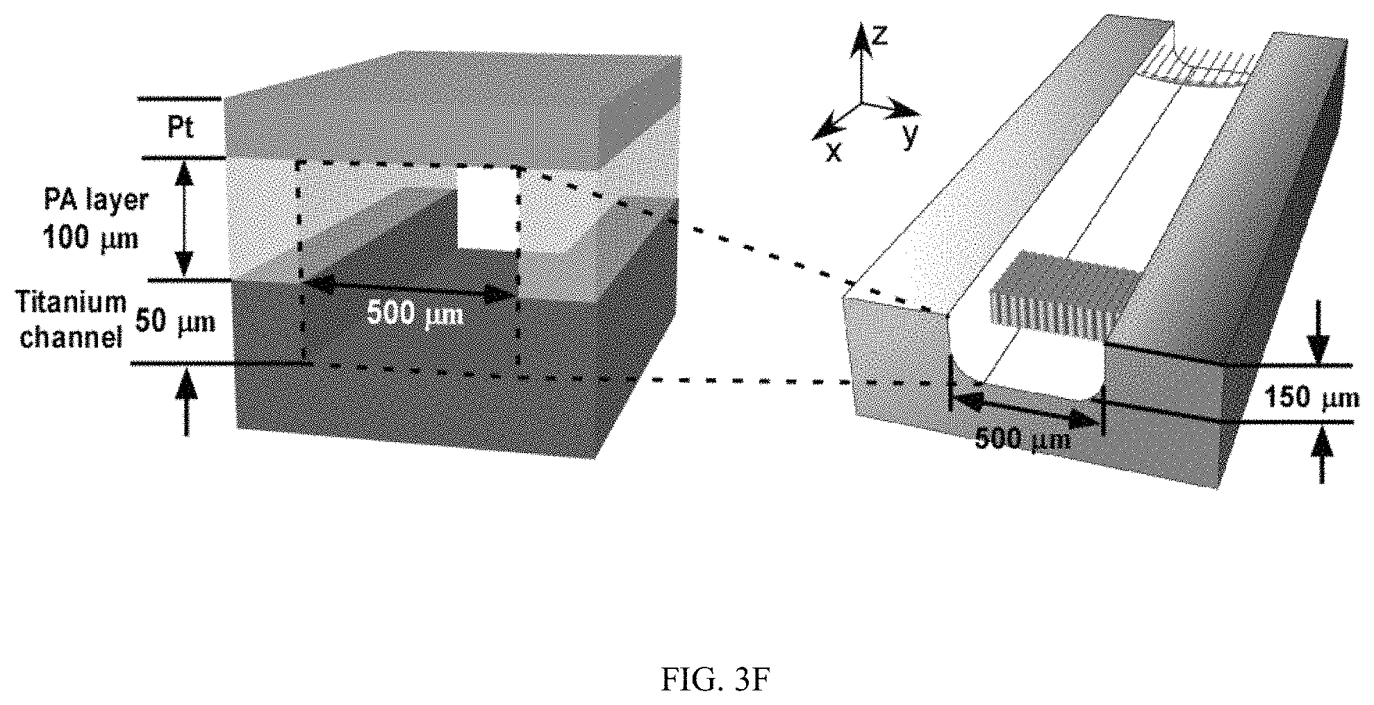
The invention has been tested experimentally by fabrication of a microfluidic device using Ti-based channels. In an embodiment, the microfluidic device used to grow TiO.sub.2 nanotubes through electrochemical anodization was composed of four parts: Ti substrate, polyacrylate film, Pt film, and polycarbonate from bottom to top. Ti served as the substrate for growing nanotubes; Pt as the cathode; polyacrylate as the isolating layer between cathode and anode; and polycarbonate served as the cover of microfluidic device.
The pattern of microchannel on Ti substrate was designed by using Solid Work software, and was then machined on the Ti substrate by a numeric controlled Bridgeport Vertical Milling machine equipped with Proto-TRAK system. Before milling, the Ti substrate were first polished and then cut into 9 pieces (1.18''.times.1.18''). Due to the high hardness of the Ti, the milling speed was set at 0.5 mm/min with a 0.2 inch endmill (TS-2-0200-S, PMT) at 3600 rpm for machining. The dimensions of the patterns of the microchannels were milled at 500 .mu.m of the width and 2 mm of the depth.
For the purpose of separating the anode and cathode but enabling the contact between electrodes and electrolyte, either polyacrylate plastic or polyester film was used as an isolating layer depending on the purpose. Laser cutting technique was applied to cut the microchannel pattern and holes for screws on the polyacrylate plastic and polyester film.
The Pt film was cut into 0.5''.times.0.5'' and embedded at the middle between the polycarbonate layer and isolating layer. A screw inserted through the polycarbonate from the top locating at the center was used to connect the Pt film with cathode electrode for electric conductivity.
The polycarbonate was cut into the size of 1.18''.times.1.18'' and used as the top layer of microfluidic device. Four corner holes for assembling screws and one center hole for cathode connecting screw were drilled through the whole part and taped. Four smaller holes (0.06'') served as inlets and outlets of fluids were drilled with good alignment with the Ti substrate pattern.
For microfluidic device fabrication, these four parts were assembled into an integrated microfluidic device by using four corner screws (#4-40, 0.089''). One additional screw (M3.times.0.5) was used to insert into the center polycarbonate part for connecting the cathode electrode with the Pt cathode embedded between polycarbonate and polyacrylate isolating layer. The anode electrode was connected with the screw located at the corner of device.
The present invention provides a process for the electrochemical anodization of titanium in an embodiment which enhances the anodic growth of TiO.sub.2 nanotubes by decreasing the electrode distance at a constant anodizing voltage. According to an embodiment, the change of nanotube structures becomes more sensitive to the electrode distance at high anodizing voltages. The process provides a correlation between electrode distance and current density during the anodic growth of TiO.sub.2 nanotubes to affect the growth of TiO.sub.2 nanotubes. The process enables in situ growth of TiO.sub.2 nanotubes in microdevices and offers a promising approach to produce TiO.sub.2 nanotube arrays in a more energy-effective manner by just decreasing the electrode distance. By decreasing the electrode distance, both the diameter and length of TiO.sub.2 nanotubes can be improved due to the enhanced steady-state current density.
A complex field-aided oxidation and dissolution process during electrochemical anodization of Ti is believed to be responsible for the formation of TiO.sub.2 nanotube arrays. The oxidation of Ti in the anode produces Ti.sup.4+ ions that migrate under the field and react with O.sup.2- ions to form the anodic TiO.sub.2 layer. Fluorides (F.sup.-) in the electrolyte, on the other hand, attack the TiO.sub.2 layer and generate water soluble TiF.sub.6.sup.2- ions, resulting in the dissolution of the TiO.sub.2 layer and initiate the formation of TiO.sub.2 nanotube arrays. Although the formation of tubular instead of porous TiO.sub.2 layer is mechanistically debatable, TiO.sub.2 nanotubes keep growing until the formation and dissolution of TiO.sub.2 reaches equilibrium. At this stage, the thickness of the TiO.sub.2 nanotube arrays, i.e., the length of TiO.sub.2 nanotubes, keeps constant although TiO.sub.2 nanotubes are penetrating deeper into the metal. Because the growth of TiO.sub.2 nanotubes is controlled by the field-aided oxidation and F.sup.--based chemical dissolution, the diameter and length of TiO.sub.2 nanotubes can be regulated by controlling the magnitude of applied electrical field, composition of the electrolyte (i.e., concentration of F.sup.-, pH, and water content) and anodization time. The outer diameter of TiO.sub.2 nanotubes, for example, increases linearly with applied voltage and long nanotubes are obtained with extended anodization.
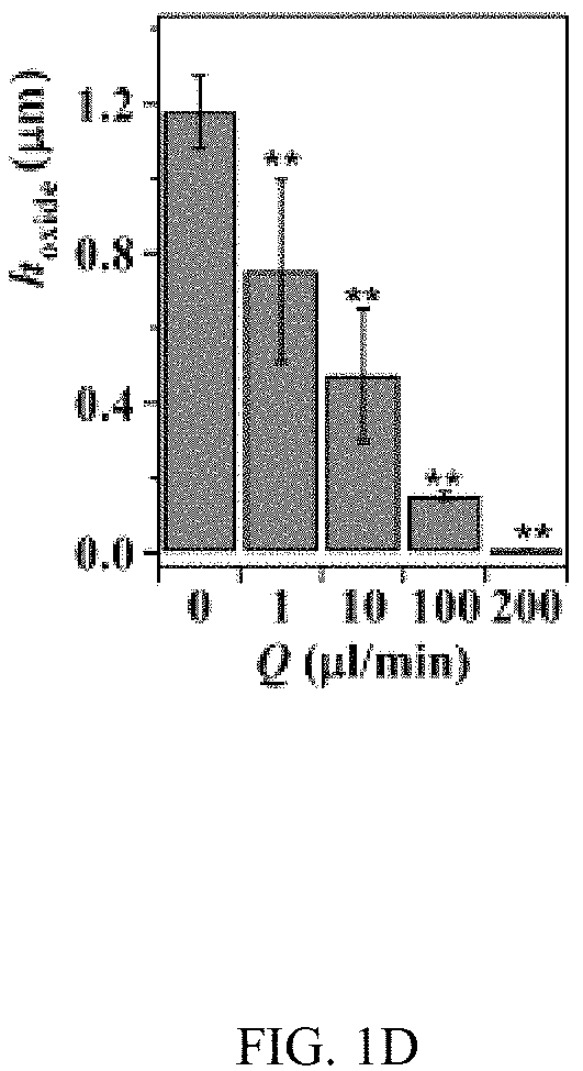
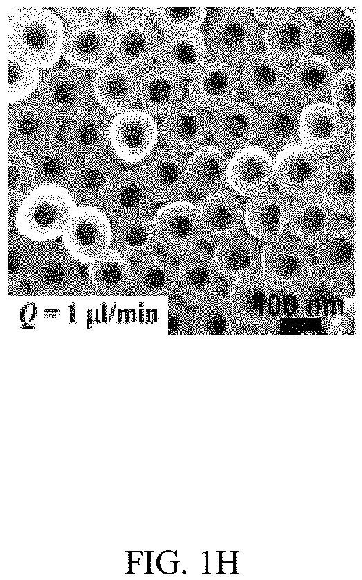
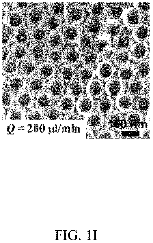
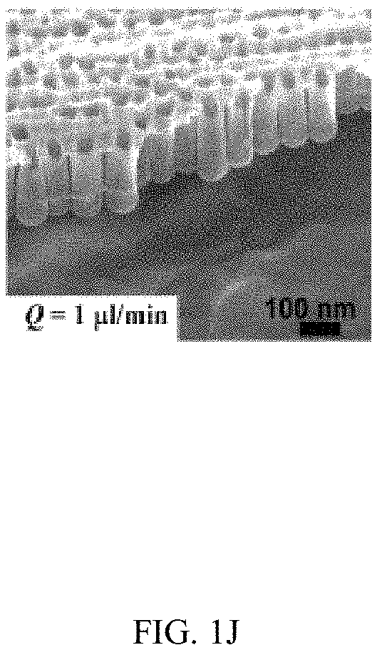
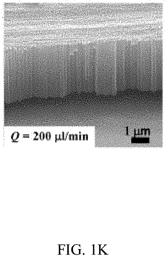
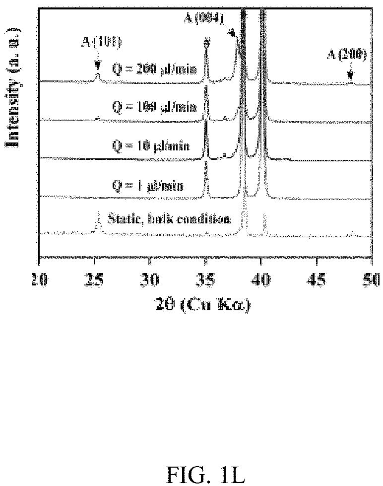
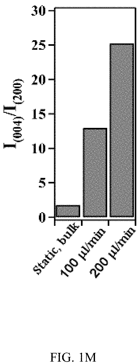
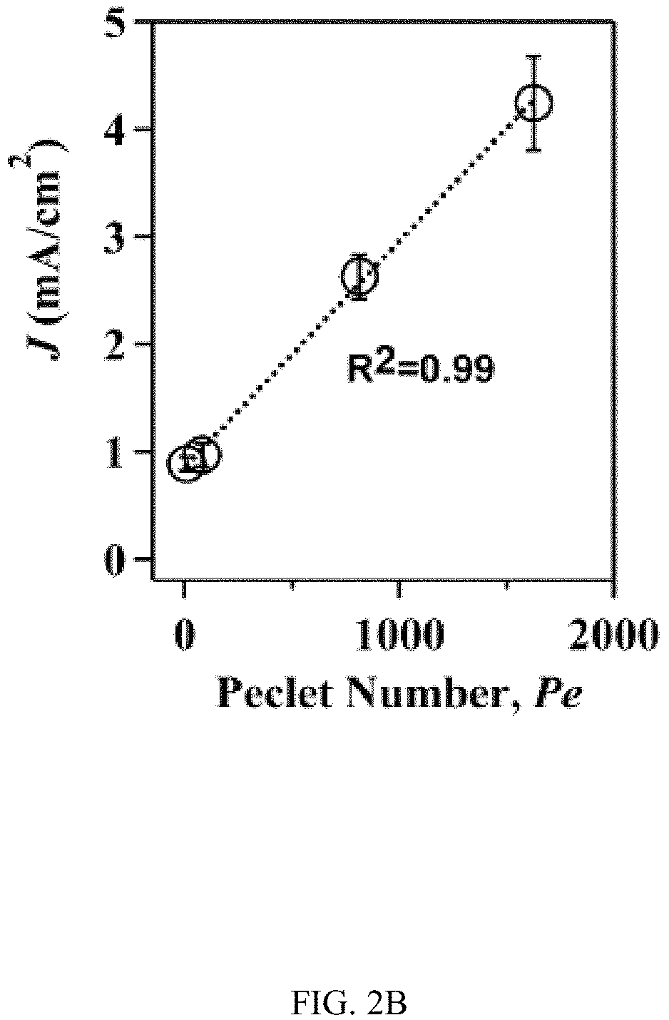
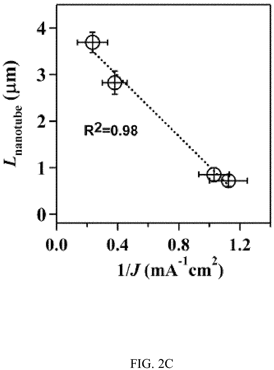
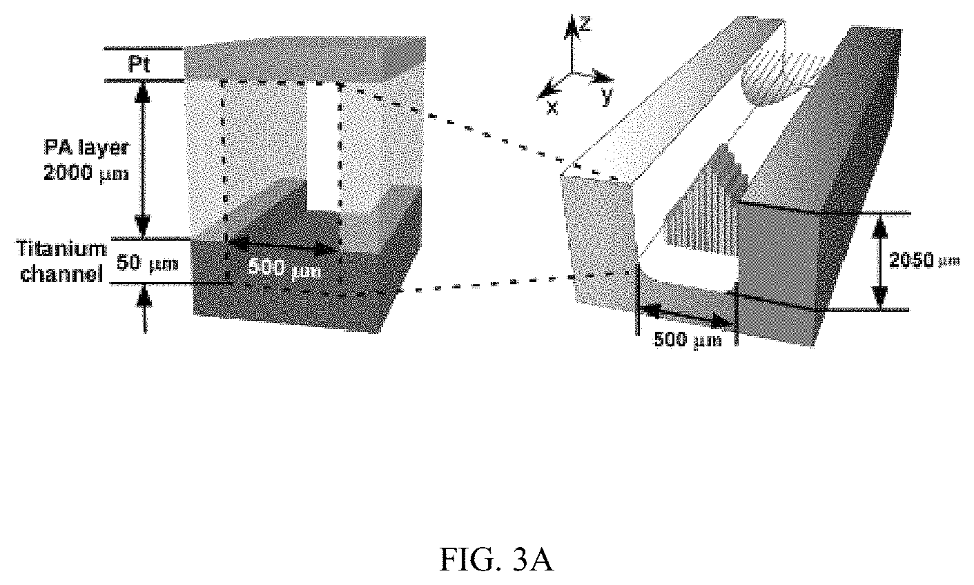
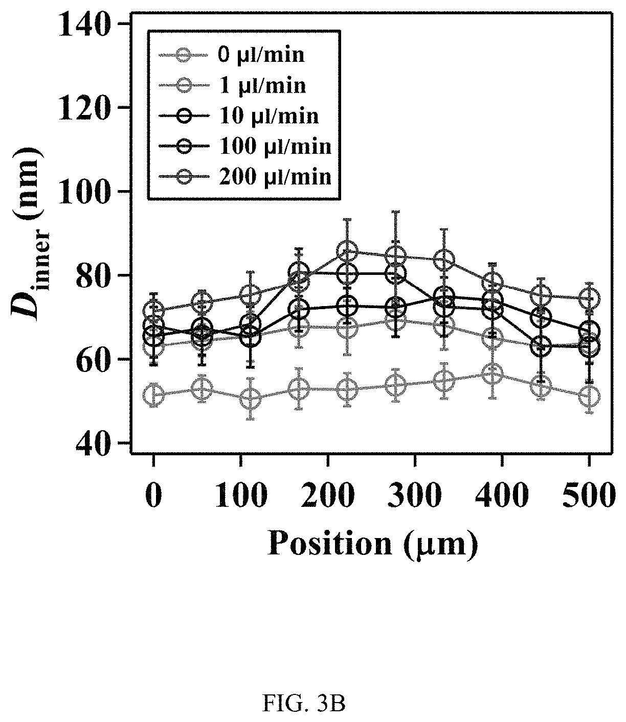
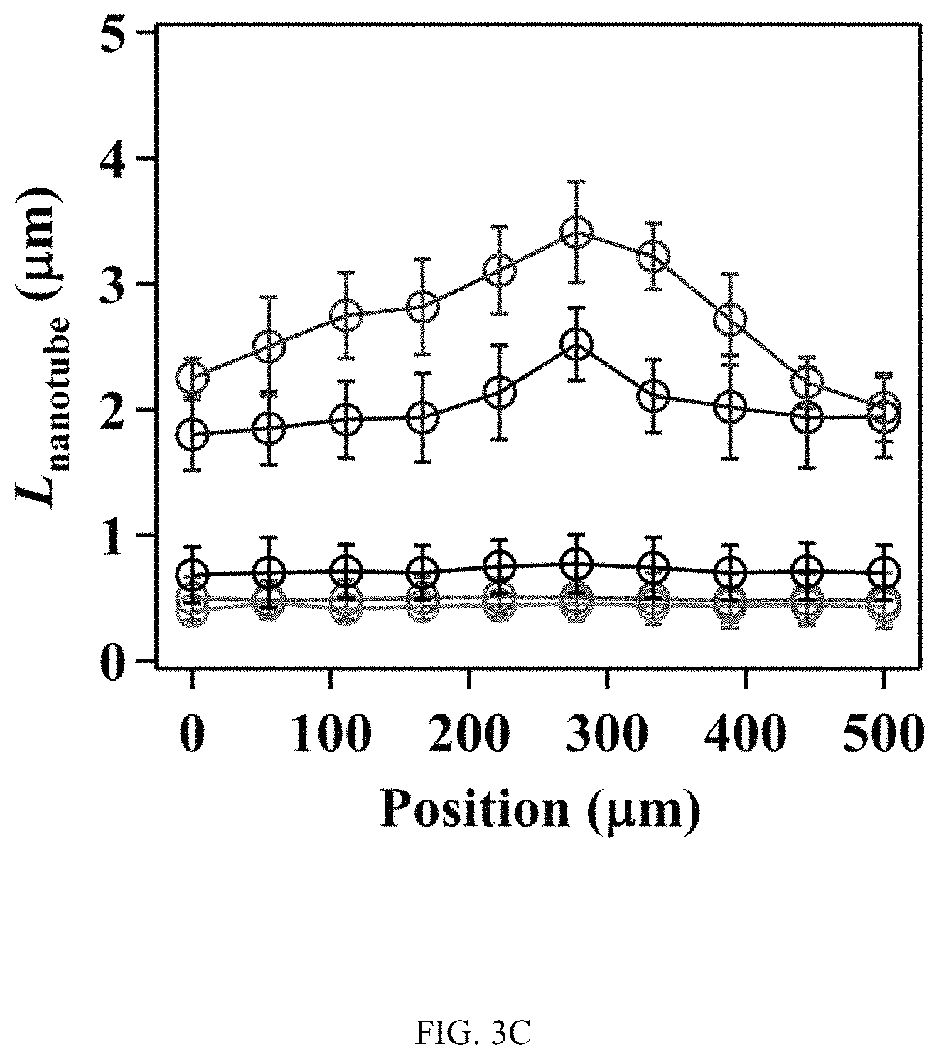
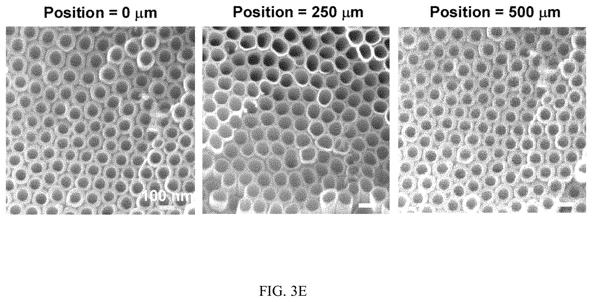
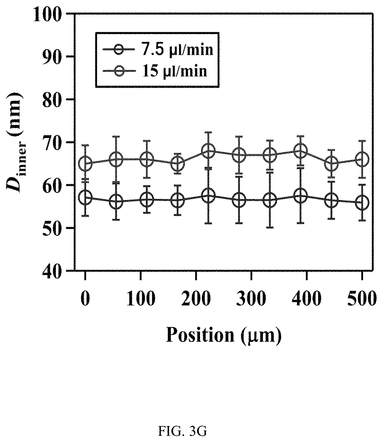
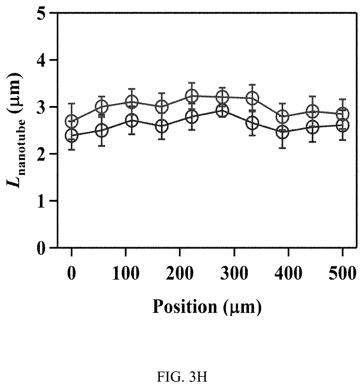
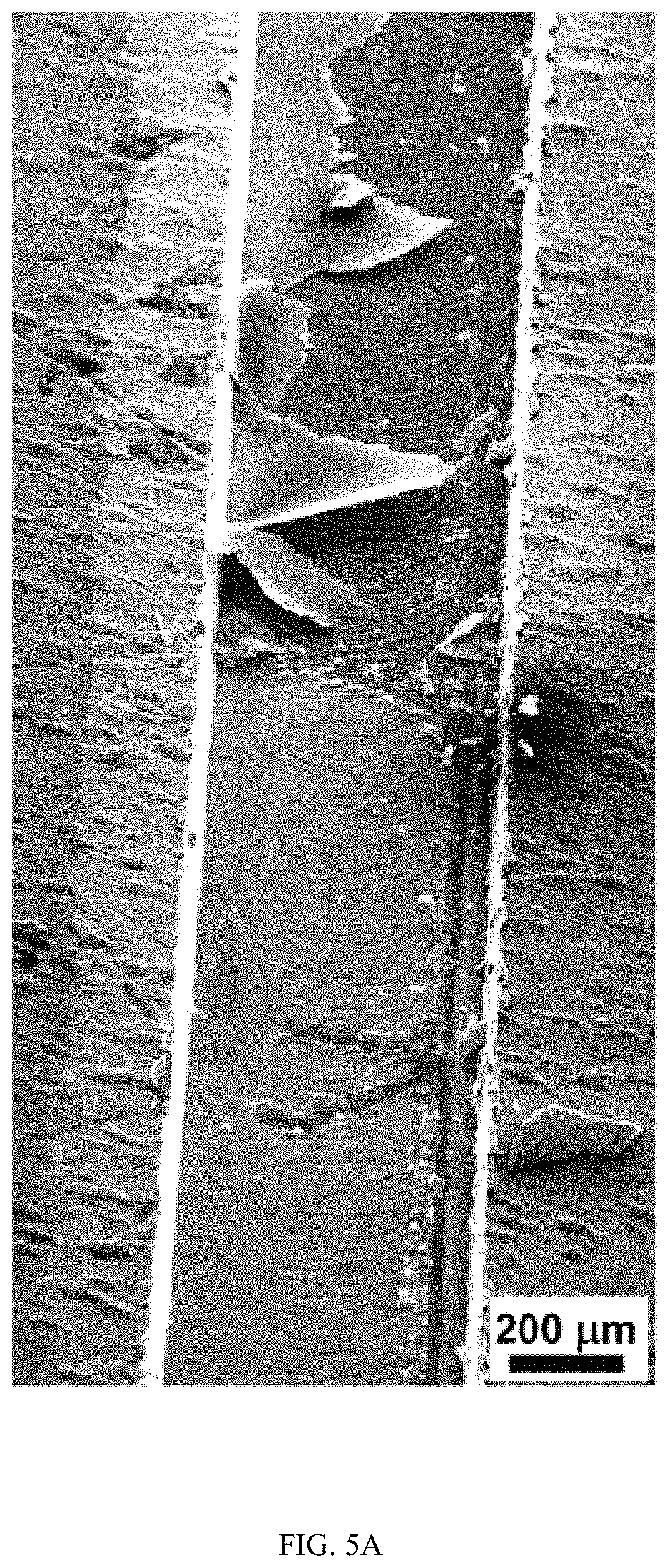
In an embodiment microfluidic channels were fabricated directly inside a metallic Ti substrate and conducted electrochemical anodization of Ti to produce TiO.sub.2 nanotube arrays under controlled flow conditions (FIGS. 1A, 1B, and 5A-5C and Table S1). The applied voltage (40V), composition of the electrolyte, and anodization time (30 min) were kept constant for all microfluidic experiments and only changed the hydrodynamic conditions in the microfluidic channel during anodization. FIG. 1C showed a typical scanning electron microscope (SEM) image of the Ti microfluidic channel covered with TiO.sub.2 nanotube arrays after anodization. Consistent with previous studies, there was a compact oxide layer on the top of the nanotube arrays (FIG. 6A). With the increase of flow rates, however, the thickness and the coverage of the compact oxide layer initially formed at the electrolyte-oxide interface decreased significantly (FIGS. 1D, 1E and 6), implying that high flow rate inhibits the formation of the compact oxide layer during anodization. In addition, although the outer diameter of the nanotube did not change significantly with flow rates, the inner diameter of the nanotube increased with flow rates (FIGS. 1F, 1H, & 1I), resulting in a decrease of wall thickness of nanotubes. Remarkably, the length of nanotubes increased up to about 400% as the flow rate was increased from 0 .mu.l/min to 200 .mu.l/min (FIGS. 1G, 1J and 1K). It is important to note that the anodization time in the current microfluidic setup is 30 min whereas it takes approximately 8-10 hours to grow similar length of nanotubes in conventional static, bulk conditions. In addition, TiO.sub.2 nanotubes produced under flow conditions have regular diameters with a narrow size distribution, suggesting that flow does not lead to inhomogeneous top structures as observed in most long-duration anodization experiments. Furthermore, when TiO.sub.2 nanotubes were annealed at 425.degree. C. and analyzed by X-ray diffraction (XRD), typical anatase TiO.sub.2 reflection peaks A(101), A(004) and A(200) were observed and the magnitude of reflection peaks increased with flow rates (FIG. 1L). In particular, comparing to nanotubes with similar length but produced under conventional static, bulk conditions, TiO.sub.2 nanotubes generated at high flow rates (e.g., 200 .mu.l/min) showed significantly increased peak intensity of A(004) and I.sub.004/I.sub.200 (FIGS. 1L and 1M), implying that the crystal growth of TiO.sub.2 nanotubes produced at flow conditions is preferentially oriented along the [001] direction. The current-time characteristics of anodization under flow conditions were examined (FIG. 2A). Current-time curves particularly at high flow rates, i.e., 200 .mu.l/min, showed typical patterns of growing TiO.sub.2 nanotubes, which included an exponential decrease of the current due to the formation of the oxide layer (stage I), followed by a slight increase of current due to the formation of initial porous structures (stage II), and then a relatively steady current due to the formation of self-organized nanotube arrays (stage III). The magnitude of the steady state current at stage III correlates to the thickness of nanotube arrays and will not increase significantly with extended anodization time unless the anodic potential is changed. Without the change of applied voltage, however, the steady state current changed with flow rates and increased linearly with Peclet number (Pe) (FIG. 2B and Table S2). Pe is defined as the ratio of the rate of convection by the flow to the rate of diffusion driven by a concentration gradient (Pe=Lu/D, where L is the characteristic length, u is the flow velocity, and D is the diffusion coefficient) and high Pe indicates a convection-dominated mass transport process. Because the length of nanotubes correlated inversely with the steady state current (FIG. 2C), the increased steady state current with Pe suggests that convection perpendicular to nanotubes plays a role in the regulation of key transport processes that are important to the growth of TiO.sub.2 nanotubes. Previous studies of anodization of Ti in static conditions showed that there were concentration gradients of F.sup.- and TiF.sub.6.sup.2- ions inside and outside the nanotubes and a diffusion layer was presenting adjacent to the top of the nanotubes. When flow is applied tangentially to the surface of nanotube arrays, the thickness of the diffusion layer, Ldiff, which can be estimated as 2 Dt or 2 D L/.mu. decreases with the increase of flow velocity u and becomes negligible at high flow velocity or Pe. In this case, convection dominates the mass transport on the top of nanotubes and local concentration of TiF.sub.6.sup.2- will approach to zero and F.sup.- concentration will be close to the bulk F.sup.- concentration in the electrolyte (FIG. 2D). The change of local concentrations of TiF.sub.6.sup.2- and F.sup.- on the top of nanotubes modifies the boundary conditions of ions transport inside the nanotubes where concentration gradients of F.sup.- and TiF.sub.6.sup.2- ions still exist. As a result, the ion-flux rates in the nanotubes are enhanced (Table S3), resulting in an increased anodization current density with flow rates (FIG. 2A). TiF.sub.6.sup.2- is the diffusion rate controlling species in the formation of nanotubes, effective removal of TiF.sub.6.sup.2- accelerates the dissolution kinetics at the bottom of the nanotube arrays, and thus produces long nanotubes at high Pe (FIGS. 1G and 1K). The increased concentration of F.sup.- on the top of nanotubes, on the other hand, facilitates the chemical etching of the top nanotubes, leading to large inner diameters as shown in FIG. 11. In addition, the flow-induced change of ion transport modifies the local electrical field during anodization and consequently the degree of preferred crystal orientation after annealing. To further demonstrate the effect of flow on the growth of TiO.sub.2 nanotubes, the diameter and length of nanotubes was measured across the microfluidic channel perpendicular to the flow direction (FIG. 3A). Because the flow was pressure-driven and the height of the channel in the z direction was larger than the width of the channel in the x direction, the flow velocity profile became parabolic in the x-y plane with the highest flow velocity in the middle of the channel. As a result, nanotubes in the middle of the channel were expected to have the largest inner diameter and length. Experimental results particularly obtained at high flow rates were consistent with the prediction (FIGS. 3B and 3C). When the height of the channel was reduced while keeping the width of channel unchanged, the parabolic flow profile switched from the x-y plane to the y-z plane and left a relatively uniform velocity distribution in the x-y plane (FIG. 3F). In this case, nanotubes with relatively uniform inner diameter and length across the channel were obtained (FIGS. 3G and 3H). Pe or flow velocity was kept approximately the same in both devices at high flow rates (Tables S4 and S2). Similar results were obtained at upstream and downstream in both devices (FIGS. 8 and 9). Results show that both the nanotube structure (length and diameter) and the spatial distribution of nanotube structure can be controlled by manipulating the magnitude and distribution of flow velocity during anodization. Suitable flow rates include flow rates sufficient to inhibit growth of an oxide layer on the nanotubes while maintain laminar flow of the electrolyte solution. Suitable flow rates include Pe numbers within a laminar flow regime above about 100 and above about 1000.
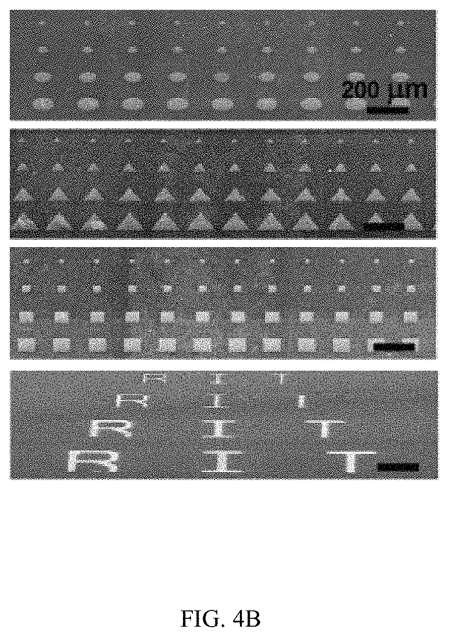
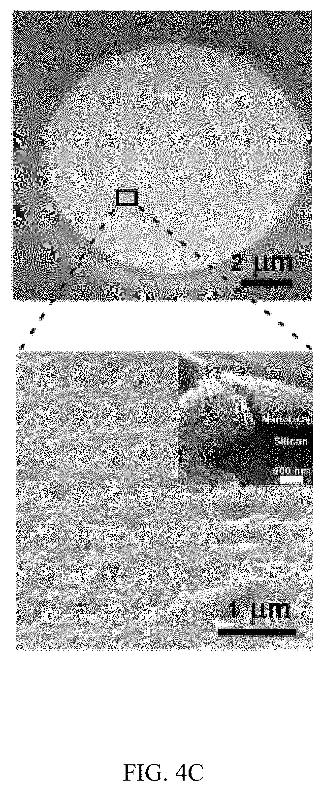
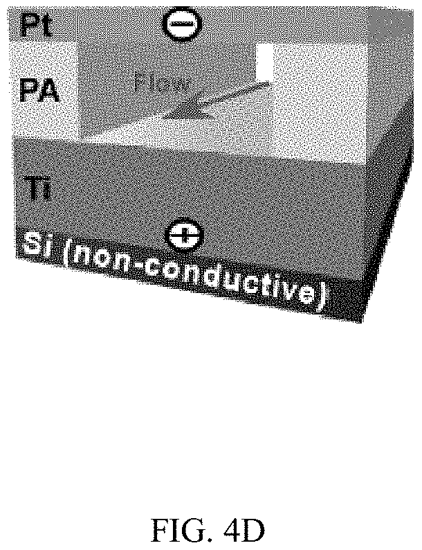
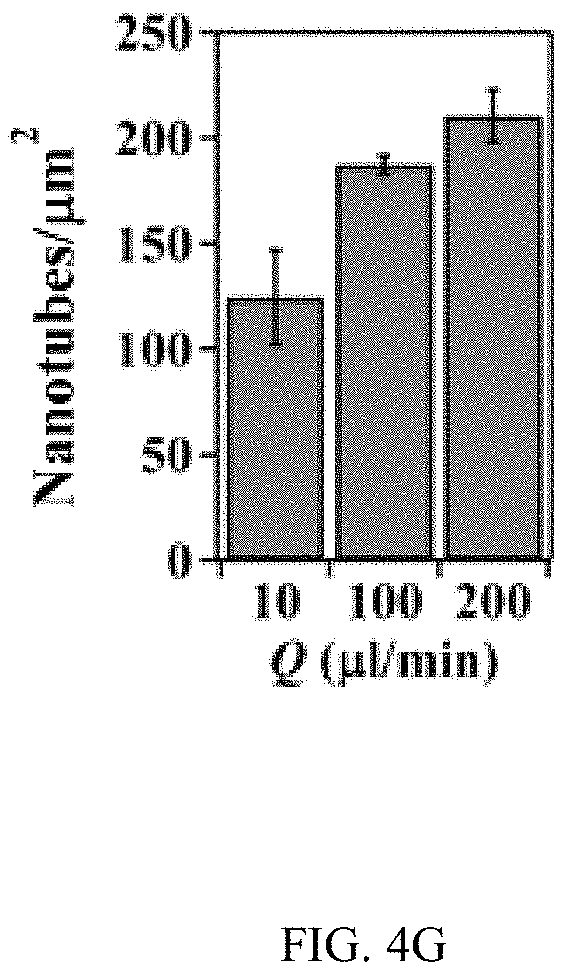
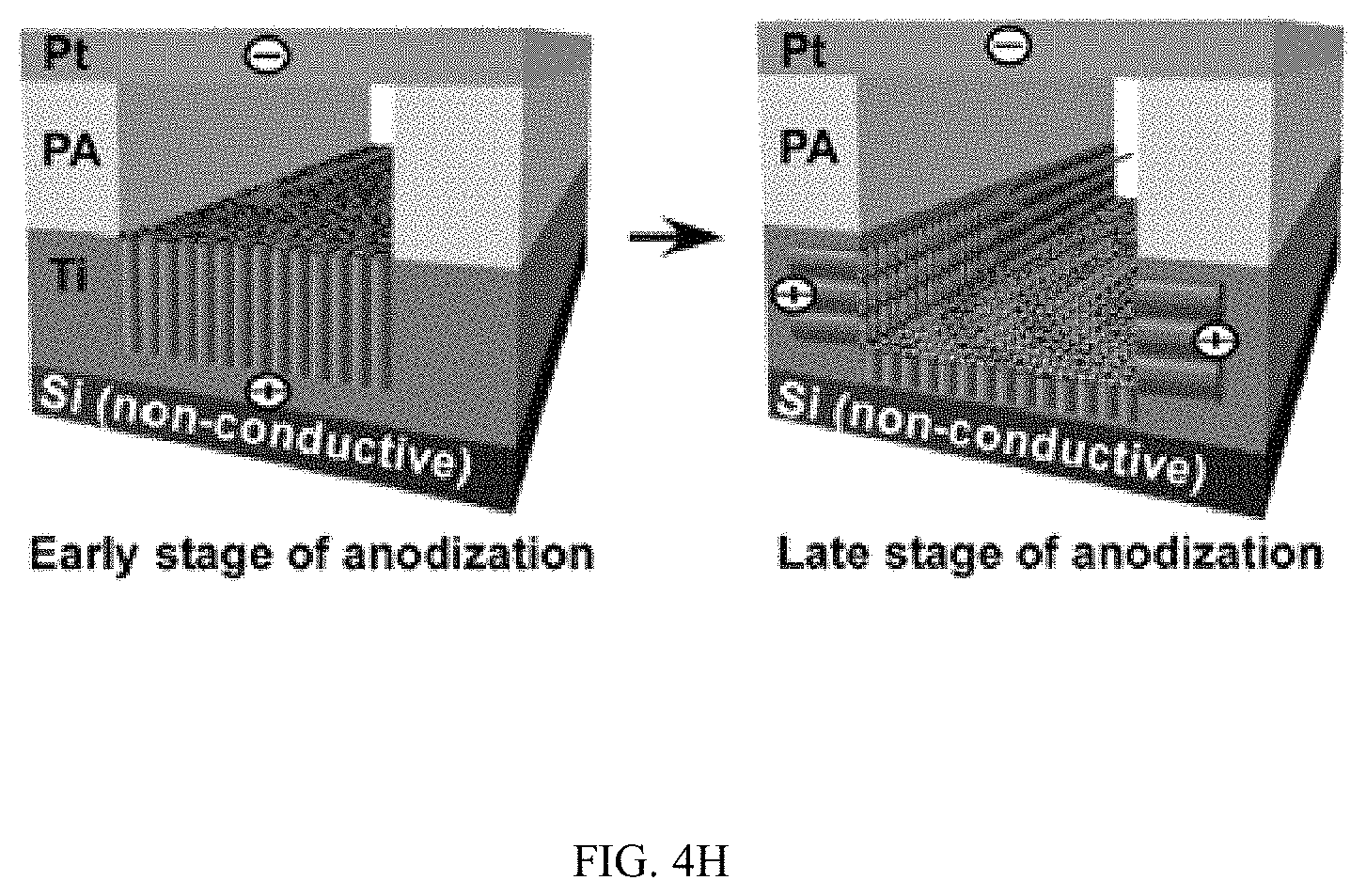
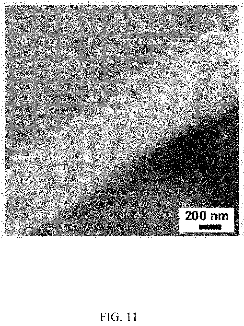
Moreover, when metallic Ti thin-film with a thickness of 500 nm was deposited on a conductive silicon substrate (.OMEGA.=1-5.times.10.sup.-3 Ohm-cm) and patterned photolithographically inside a microfluidic channel (FIG. 4A), TiO.sub.2 nanotubes could grow uniformly inside the patterned areas (FIGS. 4B and 4C). High resolution SEM images showed that nanotubes grew vertically in the patterned areas and had average diameter and length of 78.+-.5.4 nm and 304.+-.12.3 nm respectively (FIG. 4C). TiO.sub.2 nanotubes were grown microfluidically using Ti thin-film (1 .mu.m thick) deposited on a non-conductive silicon substrate (.OMEGA.=1-2.times.10.sup.4 Ohm-cm) (FIGS. 4D and 4E), horizontally aligned nanotubes were produced inside the walls of the channel after anodization (FIG. 4E top inset) while vertically aligned nanotubes were presented in the channel (FIG. 4E bottom inset). Similar phenomena were observed when a photolithographically patterned Ti layer and Ti layers with reduced thickness were used (FIG. 10). The inner diameter and density of horizontally aligned nanotubes increased with flow rates (FIGS. 4F and 4G). Horizontally aligned nanotubes were not observed on a Ti layer that was deposited on conductive silicon substrates (FIG. 11).
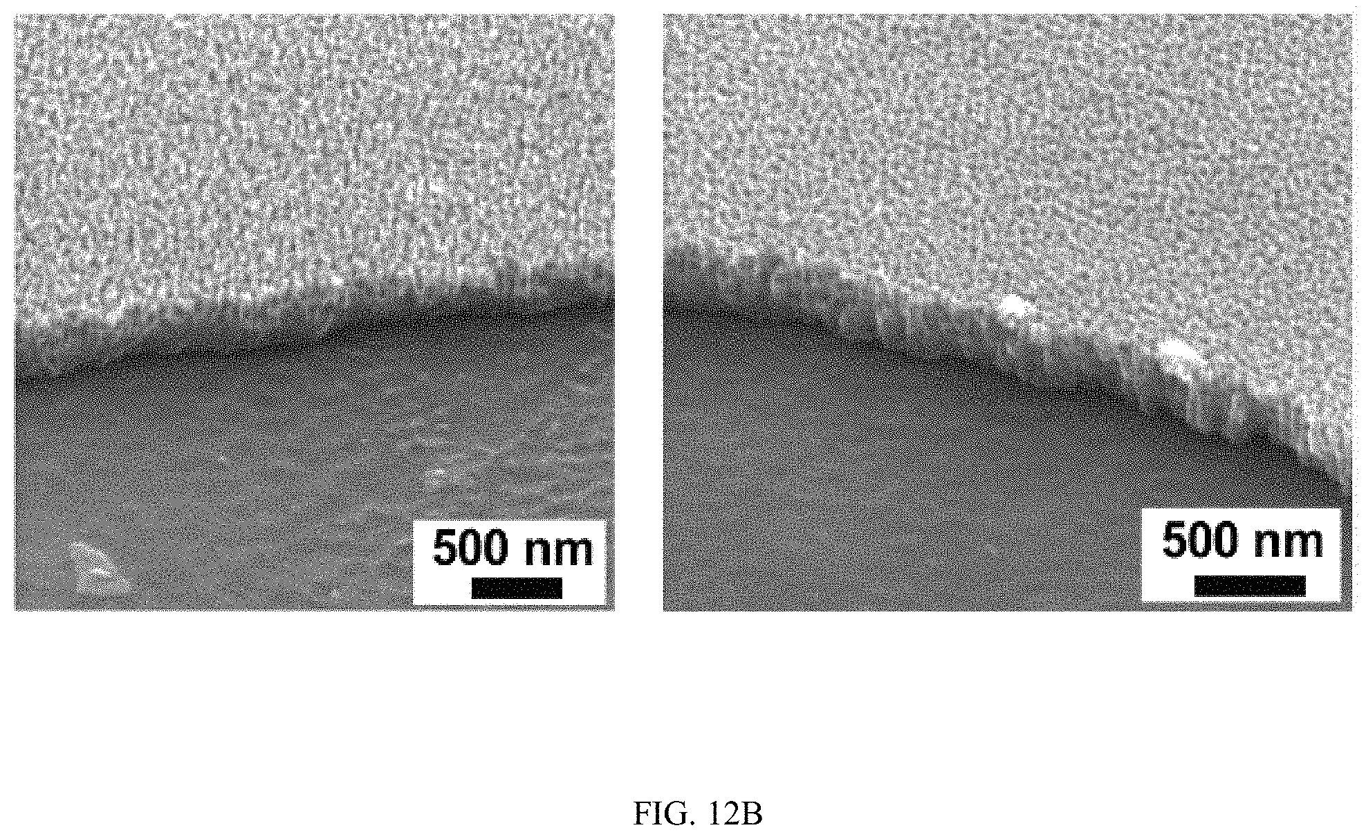
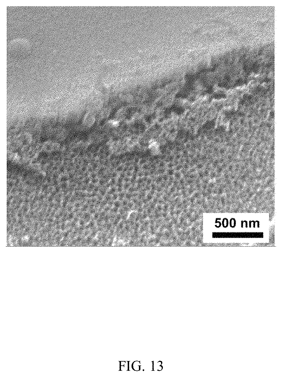
Because the growth of TiO.sub.2 nanotubes follows the direction of the electrical field during anodization, the appearance of horizontally aligned nanotubes suggests that the direction of electrical field switched to the horizontal direction during anodization. Such change is possible when a Ti layer is deposited on a non-conductive silicon substrate. In this case, when nanotubes grow throughout the entire Ti layer and reach the non-conductive silicon substrate, the electrical field in the vertical direction will change to the horizontal direction due to the presence of non-conductive silicon substrate at the bottom and the conductive Ti in the side walls (FIG. 4H). Meanwhile, the growth of TiO.sub.2 nanotubes uses the contact of Ti walls with the electrolyte solution so that field-aided reaction can penetrate into the Ti side walls to form nanotubes. This Ti-electrolyte interaction is also likely at late stages of anodization considering the continuous chemical etching on the top nanotubes and the finite thickness of the Ti layer. Indeed, at the end of anodization, the length of nanotubes inside the channel (376.+-.16.4 nm) was much smaller than the thickness of the original Ti layer (1 .mu.m) deposited on the silicon substrate (FIG. 12) and horizontally aligned nanotubes were not presenting at the early stage of anodization (5 min) (FIG. 13). The results demonstrate that by controlling the direction of the applied electrical field and the contact of Ti-electrolyte solution during anodization, TiO.sub.2 nanotube arrays can be produced with desired orientations.
The regulatory roles of flow in the anodic growth of TiO.sub.2 nanotube arrays in microfluidics showed that both the structural and material features of TiO.sub.2 nanotubes and the spatial distribution of such features could be controlled by manipulating the magnitude and distribution of flow velocity during anodization. The growth of TiO.sub.2 nanotubes was much faster in flow conditions and took approximately 56% of the time required to grow similar length of TiO.sub.2 nanotubes in conventional static conditions. Furthermore, by depositing Ti on silicon substrates, both vertically and horizontally aligned TiO.sub.2 nanotubes could be produced through microfluidics, and thus provided a powerful approach to construct hierarchical nanotube arrays on silicon-based materials. The microfluidic approaches offer a useful platform to effectively grow TiO.sub.2 nanotubes in controlled flow conditions and suggest strategies to integrate silicon with TiO.sub.2 nanotubes that may find applications in nanoelectronics, solar cells, sensors and photocatalytic devices.
An embodiment of the fabrication and assembly of a microfluidic device are shown in FIG. 1. The microchannel on a Ti substrate (2 mm thick, 99.2% pure, Alfa Aesar, Ward Mill, Mass.) was fabricated using a Bridgeport Vertical Milling machine equipped with Proto-TRAK system. The width and height of the Ti channel were 500 .mu.m and 50 .mu.m, respectively. When the Ti channel was assembled for anodization, the overall height of the microfluidic channel, which was also the approximate anode-to-cathode distance, was 150 .mu.m or 2050 .mu.m, depending on the thickness of the electrical isolation layer, i.e., the PA film. During anodization, an electrolyte solution containing 15 wt % NH.sub.4F (Sigma Aldrich), 3 ml DI water, and 145 ml ethylene glycol (VWR) was injected into the microfluidic device at different flow rates, 0, 1, 10, 100, or 200 .mu.l/min, using a syringe pump (Harvard Apparatus PhD2000). The electrochemical anodization was conducted at 40 V using an electric power supply (TKD-Lambda) for 0.5 hour at room temperature (25.degree. C.) for all microfluidic experiments. To produce TiO.sub.2 nanotubes in conventional static, bulk conditions, Ti film (0.5 mm thick, 99.2% pure, Alfa Aesar, Ward Mill, Mass.) and Pt film (0.025 mm thick, 99.9% pure, Alfa Aesar, Ward Mill, Mass.) were submerged under the electrolyte solution with a distance of 1 cm. The anodization was conducted at 60V for 30 min at room temperature (25.degree. C.). The length of TiO.sub.2 nanotubes produced under conventional static, bulk conditions have a length of 3.7.+-.0.16 .mu.m, which is similar to the length of nanotubes produced at the flow rate of 200 .mu.l/min in microfluidics. The synthesized TiO.sub.2 nanotubes were annealed at 425.degree. C. for 1 h in air using a Dual Zone Split Tube Furnace (OTF-1200X).
To grow TiO.sub.2 nanotubes on silicon substrates, a Ti thin-film was deposited on a 3'' silicon wafer (University Wafer) by using a SC4500 a-beam evaporator. For patterned geometries, the thickness of Ti thin-film was 500 nm and SU2001 photoresist (MicroChem) was spanned on the Ti thin-film via a Brewer CEE6000 automated spin coater at 3000 rpm to obtain a photoresist thickness of 1 .mu.m. The silicon wafer was doped with Boron and exhibited low electrical resistivity (.OMEGA.=1-5.times.10.sup.-3 Ohm-cm). The wafer was baked at 95.degree. C. before lithography. A quartz mask with different dimensions of circular, triangle and square shapes and logo of RIT was fabricated by using Heidelberg mask writer DWL2000. The wafer was then exposed to LTV light under the mask in an ABM contact mask aligner and developed to obtain the desired pattern on Ti. The silicon wafer with Ti coating was served as the bottom part of the assembled microfluidic device and used to grow TiO.sub.2 nanotubes. The width and height of the microfluidic channel used to grow TiO.sub.2 nanotubes in patterned areas were 1 mm and 2 mm, respectively. The flow rate was 20 .mu.l/min. To grow horizontally aligned TiO.sub.2 nanotubes, pure silicon with high electrical resistivity (.OMEGA.=1-2.times.10.sup.4 Ohm-cm) was used and Ti thin-film with a thickness of 500 nm or 1 .mu.m was deposited on the silicon wafer as described above. The width and height of the microfluidic channel were 1 mm and 2 mm, respectively. The flow rate was 0, 1, 10, 100, or 200 .mu.l/min. The Reynolds number for all the experiments varied from 9.times.10.sup.-3 to 1.9. Suitable laminar flow includes a Reynolds number of less than about 2000.
A scanning electron microscope (FIB-SEM, Zeiss Cross Beam) was used to image the TiO.sub.2 nanotubes. Nanotubes were etched with HCl (37%, Sigma Aldrich) for 2-5 min and cleaned with acetone before imaging. Energy Dispersive X-ray Spectroscopy (EDS) was conducted to analyze the presence of Ti and oxygen elements in the nanotubes. X-ray diffraction (XRD) was conducted with a Philips X'Pert MRD diffractometer (Spectris plc) using a long-fine-focus Cu Ka radiation source at 40 kV and 30 mA. The scanning range of 2.theta. was set from 20.degree. to 50.degree. with a 0.03.degree. step size. The crystalline structures of TiO.sub.2 nanotubes were identified by comparison and analysis with FIZ/NIST Inorganic Crystal Structure Database.
FIGS. 1A-1K illustrates the effect of flow on the growth of TiO.sub.2 nanotubes in microfluidics. FIG. 1A is a schematic of the generation of TiO.sub.2 nanotubes via electrochemical anodization under flow conditions. FIG. 1B shows a bright-field image of an embodiment of an assembled microfluidic device. The schematic image (right insert) shows the microfluidic device that is assembled by a titanium (Ti) substrate, a polyacrylate (PA) film, a Pt foil, and a block of polycarbonate (PC). The PA film acts as an isolating layer between the cathode (Pt) and the anode (Ti). The PC block serves as the cover of the microfluidic device. Four screws inserted through the corners of the PC block to the Ti substrate act as the anode electrodes. An additional screw that is inserted at the center of the device and connects the Pt foil serves as the cathode electrode. The enlarged image (below insert) shows the microfluidic channel fabricated on Ti by micromachining. The width and height of the channel are 500 .mu.m and 50 .mu.m, respectively. FIG. 1C is a representative SEM image of a TiO.sub.2 nanotube-covered microfluidic channel prepared with a flow rate of 200 .mu.l/min. FIG. 1D is a graph of the change of thickness of the oxide layer with flow rates. FIG. 1E is a graph of the percentage of the oxide coverage at different flow rates in the microfluidic channel. FIG. 1F is a graph of the effect of flow rates on the inner and outer diameters of TiO.sub.2 nanotubes. FIG. 1G is a graph of the effect of flow rates on the length of TiO.sub.2 nanotubes. FIGS. 1H & 1I are SEM images of a top view of TiO.sub.2 nanotubes fabricated at the flow rate of 1 .mu.l/min and 200 .mu.l/min, respectively. FIGS. 1J & 1K are SEM images of a side view of TiO.sub.2 nanotubes fabricated at the flow rate of 1 .mu.l/min and 200 .mu.l/min, respectively. FIG. 1L shows XRD patterns of annealed TiO.sub.2 nanotubes generated at different flow rates and in static, bulk condition. Note that nanotubes generated at static conditions have a similar length as that produced at Q=200 .mu.l/min. Reflection peaks from Ti are labelled by #. FIG. 1M is a graph of the intensity ratio I.sub.004/I.sub.200 of TiO.sub.2 nanotubes generated at different conditions. TiO.sub.2 nanotubes produced at high flow rates showed preference crystal orientation (004) after annealing at 425.degree. C.
FIGS. 2A-2D illustrates the effect of flow on the current density during anodization. FIG. 2A shows current-time curves during the growth of TiO.sub.2 nanotubes at different flow rates. I, II, and III indicate different growth stages. The steady state current at stage III correlates to the length of nanotubes. FIG. 2B indicates steady current density at stage III increases linearly with Peclet number (Pe=Lu/l), where L is the width of the channel, u is the velocity of the fluid, and D is the diffusion coefficient). The dotted line is a linear regression fitting curve with a correlation coefficient of 0.99. FIG. 2C indicates the length of TiO.sub.2 nanotubes correlates reciprocally with the average steady current density. The dotted line is a linear regression fitting curve with a correlation coefficient of 0.98. FIG. 2D illustrates the schematics of the regulatory roles of flow in the growth of TiO.sub.2 nanotubes. Flow at high Pe reduces the thickness of the diffusion layer on the top of the nanotubes and thus modifies boundary conditions, i.e., [F.sup.-].sub.Local.apprxeq.[F.sup.-].sub.Bulk and [TiF.sub.6.sup.2-].sub.Local.apprxeq.0, resulting in an enhanced ion flux inside the nanotube.
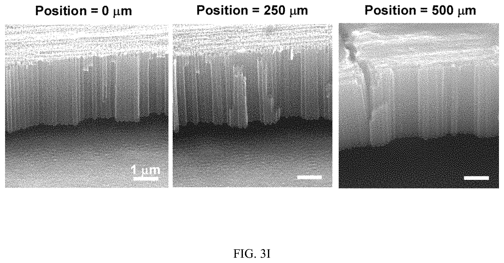
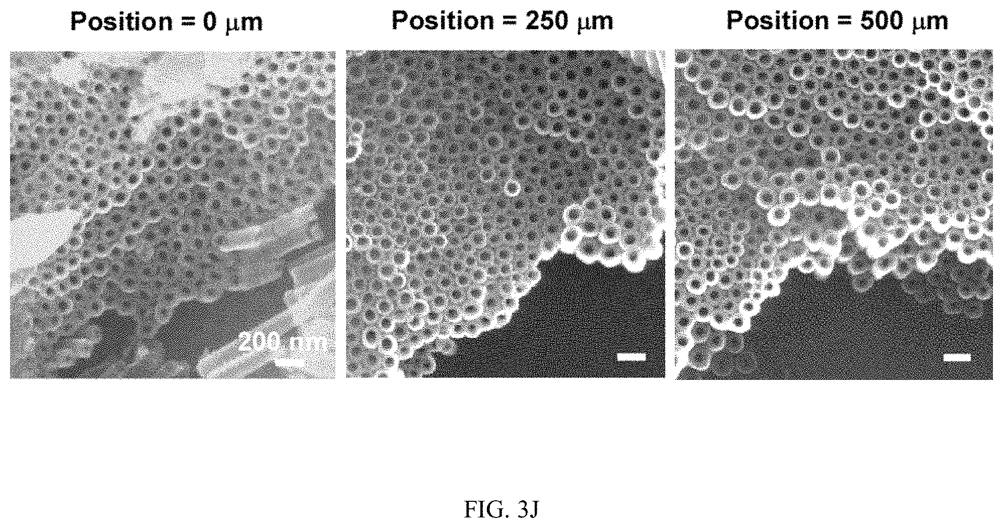
FIGS. 3A-3J illustrates the effect of flow on the spatial growth of TiO.sub.2 nanotubes in microfluidics. FIG. 3A shows the schematics of the cross-sectional view of a microfluidic channel with a width of 500 um and a height of 2050 um. The height of channel is much larger than the width of channel, the velocity profile of the flow is thus parabolic in the x-y plane. As a result, nanotubes with large inner diameter (FIG. 3E) and length (FIG. 3D) in the center of channel are expected. The change of inner diameter, shown in FIG. 3B, and length, shown in FIG. 3C, of TiO.sub.2 nanotubes, respectively, across the width of the channel at different flow rates in the microfluidic device shown in FIG. 3A. FIG. 3F shows the schematics of the cross-sectional view of a microfluidic channel with a width of 500 um and a height of 150 um. In this case, the height of channel is smaller than the width of channel, the velocity profile of the flow is parabolic in the y-z plane but flat in the x-y plane, and thus nanotubes with relatively uniform diameter (FIG. 3J) and length (FIG. 3I) across the channel width are expected. The change of inner diameter, shown in FIG. 3G, and length, shown in FIG. 3H, of TiO.sub.2 nanotubes, respectively, across the width of a channel at flow rates of 7.5 .mu.l/min and 15 .mu.l/min in the microfluidic device shown in FIG. 3F. Flow rates of 7.5 .mu.l/min and 15 .mu.l/min in the device shown in FIG. 3F provide similar flow velocity and Pe as the flow rates of 100 .mu.l/min and 200 .mu.l/min in the device shown in FIG. 3A, respectively. See Tables S2 and S4.
TABLE-US-00001 TABLE S1 EDS analysis of element composition of the Ti area and Ti0.sub.2 nanotubes in microfluidics At. Line s. Mass Mass Norm. Atom Element No. (KeV) [%] [%] [%] Ti area Oxygen 8 K-Serie: 0.5249 16.90 14.13 32.99 Titanium 22 L-Serie: 0.4522 102.70 85.87 67.01 TiO.sub.2 area Oxygen 8 K-Serie: 0.5249 46.50 34.99 61.69 Titanium 1.1 L-Serie: 0.4522 86.40 65.01 38.31
TABLE-US-00002 TABLE S2 Calculation of Pe in the microfluidic device with a height of 2050 .mu.m Flow rate Q (.mu.l/min) 1 10 100 200 Width of channel 500 L (.mu.m) Height of channel 2050 H (.mu.m) Cross-section area 1.03 .times. 10.sup.-6 A (m.sup.2) Average velocity 1.62 .times. 10.sup.-5 1.62 .times. 10.sup.-4 1.62 .times. 10.sup.-3 3.24 .times. 10.sup.-3 U = Q/A (m/s) Diffusivity 1 .times. 10.sup.-9 D (m.sup.2/s) Pe = UL/D 8.1 81 810 1620
TABLE-US-00003 TABLE S3 Calculation of diffusion flux inside the TiO.sub.2 nanotuhes Static Flow [TiF.sub.6.sup.2-] at the bottom of 1.4 .times. 10.sup.-4 1.4 .times. 10.sup.-4 nanotubes C.sub.b(M) [TiF.sub.6.sup.2-] at the top of 5 .times. 10.sup.-5 0 nanotubes C.sub.o(M) Length of nanotubes 4 4 dx (.mu.m) Diffusivity 1 .times. 10.sup.-9 D (m.sup.2/s) Diffusion flux 2.25 .times. 10.sup.-5 3.5 .times. 10.sup.-5 J (mole/m.sup.2 s) % increase of J in flow 56% (J.sub.flow-J.sub.static/J.sub.static)
TABLE-US-00004 TABLE S4 Calculation of Pe in the microfluidic device with a height of 150 um Flow rate Q (.mu.l/min) 7.5 15 Width of channel 500 L (.mu.m) Height of channel 150 H (.mu.m) Cross-section area A 7.5 .times. 10.sup.-8 (m.sup.2) Average velocity 1.62 .times. 10.sup.-3 3.34 .times. 10.sup.-3 U = Q/A (m/s) Diffusivity 1 .times. 10.sup.-9 D (m.sup.2/s) Pe = UL/D 835 1670
FIGS. 4A-4H illustrates control of the growth of TiO.sub.2 nanotubes on silicon substrates. FIG. 4A a schematic of the growth of TiO.sub.2 nanotubes on a conductive silicon substrate (.OMEGA.=1-5.times.10.sup.-3 Ohm-cm) with photoligraphically patterned goemetries. FIG. 4B is a series of SEM images of TiO.sub.2 nanotubes grown in patterned circle, triangle, square and logo of "RIT", respectively, with a flow rate of 20 .mu.l/min. FIG. 4C are high resolution SEM images of TiO.sub.2 nanotubes grown in patterned circular shape. Images below show the top view and side view (inset) of TiO.sub.2 nanotubes inside the circular pattern. FIG. 4D is a schematic of growth of TiO.sub.2 nanotubes on a non-conductive silicon substrate (.OMEGA.=1-2.times.10.sup.4 Ohm-cm) in a microfluidic channel. FIG. 4E is a representative SEM image of growing TiO.sub.2 nanotubes on a nonconductive silicon substrate. The dark area indicates the channel where anodization occurs. The gray areas show Ti coated on silicon where no anodization occurs. Flow rate: 200 .mu.l/min. The upper inset is an SEM image of the edge of the channel where Ti in the wall was anodized to produce horizontally oriented TiO.sub.2 nanotubes. The lower inset is an SEM image of TiO.sub.2 nanotubes growing in the center of the microfluidic channel. FIGS. 4F & 4G show the change of inner diameter of horizontally oriented TiO.sub.2 nanotubes and the number of nanotubes per area inside the side wall of the channel, respectively. FIG. 4H is a schematic of the growing mechanism of horizontally aligned TiO.sub.2 nanotubes on a non-conductive silicon substrate. The change of the direction of the electrical field and exposure of Ti side walls to the electrolyte flow at late stages of anodization are likely responsible for the observed horizontally-aligned TiO.sub.2 nanotubes.
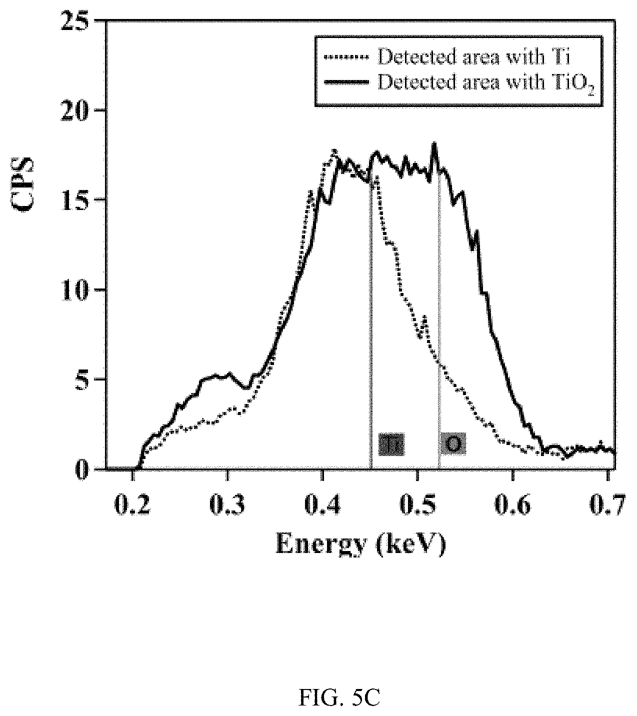
FIGS. 5A-5C show the characterization of TiO.sub.2 nanotubes using energy dispersive X-ray spectroscopy (EDS). FIG. 5A is an SEM image of TiO.sub.2 nanotube-covered microfluidic channel. The layer of TiO.sub.2 nanotubes was mechanically scratched to expose the underneath Ti substrate. FIG. 5B is an SEM image of the EDS analysis in selected areas of the TiO.sub.2 nanotube-covered microfluidic channel. Green color represents oxygen element in the sample. FIG. 5C is a graph of intensity of Ti and O element at different energy levels. The Ti/O ratio is estimated to be 1:2 from the ratio of the peak height of O (0.452 keV) and Ti (0.523 keV).
FIGS. 6A and 6B show the effect of flow on the growth of the oxide layer formed at the oxide-electrolyte interface. FIGS. 6A & 6B show the typical SEM images of the oxide layer formed under a flow rate of 1 .mu.l/min and 200 .mu.l/min, respectively.
FIGS. 7A (0 .mu.l/min), 7B (1 .mu.l/min), 7C (10 .mu.l/min), 7D (100 .mu.l/min) and 7E (200 .mu.l/min) are graphs of flow rate verses inner diameter of TiO.sub.2 nanotubes produced through anodization in a microfluidic device.
FIGS. 8A-8C shows the effect of flow on the spatial growth of TiO.sub.2 nanotubes in microfluidics at different locations along the microfluidic channel. FIG. 8A is a schematic of the microchannel. Arrows indicate the flow direction. The change of length FIG. 8B upstream and FIG. 8C downstream across the width of microchannel fabricated at different flow rates, as indicated. The width and height of the channel are 500 .mu.m and 2050 .mu.m, respectively.
FIGS. 9A-9C shows the effect of flow on the spatial growth of TiO.sub.2 nanotubes in microfluidics at different locations along the microfluidic channel. FIG. 9A is a schematic of the microchannel. Arrows indicate the flow direction. The change of length at FIG. 9B upstream and FIG. 9C downstream across the width of microchannel fabricated at flow rates of 7.5 .mu.l/min and 15 .mu.l/min. The width and height of the channel are 500 .mu.m and 150 .mu.m, respectively.
FIGS. 10A-10C shows the horizontal growth of TiO.sub.2 nanotubes on non-conductive silicon substrates. FIG. 10A shows the growth of TiO.sub.2 nanotubes using a single microfluidic channel. The thickness of Ti coating is 500 nm. The width and the height of channel are 1 mm and 2 mm, respectively. Flow rate: 200 .mu.l/min. FIG. 10B shows the growth of TiO.sub.2 nanotubes using a double microfluidic channel. The thickness of Ti coating is 500 nm. The width and the height of the channel are 1 mm and 2 mm, respectively. The distance between channels is 1 mm. Flow rate: 200 .mu.l/min. FIG. 10C shows the growth of TiO.sub.2 nanotubes on SPR 220 3.0 photoresist patterned surfaces using a single microfluidic channel. The width and the height of the channel are 1 mm and 2 mm, respectively. The thickness of the SU-8 pattern is 3 .mu.m. Inset: dark area was Ti layer that was exposed to flow to produce TiO.sub.2 nanotubes.
FIG. 11 is an SEM image of TiO.sub.2 nanotubes grown on a conductive silicon substrate. The SEM image shows the microfluidic channel wall when anodization of Ti was conducted on a conductive silicon substrate for 30 min.
FIGS. 12A-12B show TiO.sub.2 nanotubes growing on a non-conductive silicon substrate. SEM images in FIG. 12A show the exposure of sidewalls of microfluidic channel at the end of anodization. FIG. 12B show SEM images of TiO.sub.2 nanotubes in the center of the microchannel with a much shorter length (376+16.4 nm) comparing to the original thickness (1 .mu.m) of the Ti film.
FIG. 13 shows early stage of the growth of TiO.sub.2 nanotubes on a non-conductive silicon substrate. The SEM image shows the nanotubes only grow vertically at the center of the microfluidic channel and no horizontal growth of nanotubes in the side walls are observed at the anodization time of 5 min.
FIGS. 14A-14C illustrate electrode distance regulates the anodic growth of TiO.sub.2 nanotube. FIG. 14A shows a schematics of the anodic growth of TiO.sub.2 nanotubes. The anodizing voltage (V) is kept at 20, 40 or 60V. The distance between the cathode (Pt) and anode (Ti) (d) varies at 5, 1, 0.2, or 0.05 cm for each anodizing voltage. SEM images of FIG. 14B top view and FIG. 14C side view of TiO.sub.2 nanotubes fabricated at 60V when the electrode distance is controlled at 5, 1, 0.2, or 0.05 cm.
FIGS. 15A-C show the effect of electrode distance (d) on the growth of TiO.sub.2 nanotubes at different anodizing voltages. The dependence of FIG. 15A length (L), FIG. 15B inner diameter (ID) and FIG. 15C outer diameter (OD) of TiO.sub.2 nanotubes on d at an anodizing voltage of 20, 40 or 60V. **P<0.01, *P<0.05, and non-significant (NS) were calculated based on paired t-test analysis.
FIGS. 16A-16B show electrode distance (d) regulates current density (J) during the anodic growth of TiO.sub.2 nanotubes. FIG. 16A shows change of current density with electrode distance when anodizing voltage is 60V. FIG. 16B shows the dependence of steady-state current density on d at different anodizing voltages. **P<0.01 was calculated based on paired t-test analysis.
FIGS. 17A-17C shows inverse of the current density (J) correlates linearly with the structure of TiO.sub.2 nanotubes. The dependence of FIG. 17A length (L), FIG. 17B inner diameter (ID) and FIG. 17C outer diameter (OD) of TiO.sub.2 nanotubes on 1/J at an anodizing voltage of 20, 40, or 60V.
The invention will be further illustrated with reference to the following specific examples. It is understood that these examples are given by way of illustration and are not meant to limit the disclosure or the claims to follow.
Example 1
An assembled microfluidic device was fabricated for growing and regulating titanium dioxide (TiO.sub.2) nanotubes in flow condition, as shown in FIGS. 1A-1M. The device is composed of six parts: Ti substrate (Anode) with microchannel pattern, polyacrylate (PA) insulating layer with microchannel pattern, Platinum (Pt) as cathode, polycarbonate top cover, metal screws and polyethylene tubing. The microchannel on Ti substrate was fabricated using Bridgeport Vertical Milling machine with 500 .mu.m and 50 .mu.m for width and height respectively. The other parts were engineered through either machining or laser cutting. Different parts were assembled into an integrated device by using screws.
Electrolyte solution was injected at flow rate of 1, 10, 100, or 200 .mu.l/min through the microchannel via tubing and syringe pump. As a result, the thickness of oxide layer on top of the nanotubes and the percentage of oxide coverage were found to decrease with the increasing flow rates. In addition, the dimensions including the inner diameter and length of nanotubes were improved by applying flow condition at increasing flow rate, for example, the length was increased up to about 4000% as the flow rate increased from 0 to 200 .mu.l/min. Moreover, flow condition was able to regulate the crystal orientation during the X-ray diffraction measurements and the crystal growth of nanotubes produced at flow condition is preferentially oriented along the [001] direction. Collectively, the structural (e.g., length and diameter) and material (e.g., crystal orientation) properties of TiO.sub.2 nanotubes can be controlled by changing the magnitude of flow rate in microfluidics during anodization.
Example 2
During the anodization in microfluidic device, current-time curves particularly at high flow rate showed the typical patterns of the anodic growth of TiO.sub.2 nanotubes, as shown in FIGS. 2A-2D. Without the change of the applied voltage, we showed that the steady-state current changed with flow rate and increased linearly with Peclet number (Pe). High Pe indicates a convection-dominated mass transport process. Because the length of the nanotubes correlates with the steady-state current, the increased steady-state current with Pe suggests that convective flow on the top of nanotube arrays plays a role in the regulation of key transport processes that are important to the growth of TiO.sub.2 nanotubes.
Example 3
During the anodization of TiO2 nanotubes in microfluidic device, flow velocity profile was found to be able to regulate the dimension of nanotubes, as shown in FIGS. 3A-3J. When the height of the channel in the z direction is larger than the width of the channel in they direction, the velocity profile of the flow (in the x direction) is parabolic in the x-y plane with the highest flow velocity in the middle of the channel. As a result, nanotubes in the middle of channel were produced with larger inner diameter and length. When the height of channel is reduced while keeping the width of the channel unchanged, the parabolic flow profile switched from the x-y plane to the x-z plane and left a relatively uniform velocity distribution in the x-y plane. Thus the nanotubes could be produced with relatively uniform inner diameter and length across the channel. Collectively, the spatial distribution of nanotube structure in microfluidics can be controlled by manipulating the flow velocity profile during anodiazation.
Example 4
A conductive silicon substrate (.OMEGA.=1-5.times.10.sup.-3 Ohm-cm) with the deposition of a 500 nm thickness metallic Ti thin-film was used as substrate instead of Ti substrate for the anodization in microfluidics as shown in FIGS. 4A-4H. Nanotubes could be controllably patterned into different geometries through using photolighrgraphy and the nanotubes were fabricated with an average diameter and length of 78 nm and 304 nm, respectively. Remarkably, when TiO.sub.2 nanotubes were anodized microfluidically on a Ti thin-film (1 .mu.m thick) that was deposited on a non-conductive silicon substrate (.OMEGA.=1-2.times.10.sup.4 Ohm-cm), horizontally-aligned nanotubes relative to the silicon substrate were produced inside the walls of the channel while vertically-aligned nanotubes were present in the center of the channel. In addition, the inner diameter and density of horizontally-aligned nanotubes increased with flow rate. Therefore, the alignment of nanotube growth in microfluidics can be regulated when a Ti-coating non-conductive silicon substrate is applied.
Example 5
Characterization of TiO.sub.2 nanotubes using energy dispersive X-ray spectroscopy (EDS) was conducted to determine the elemental property of nanotubes, as shown in FIGS. 5A-5C. Green color represents oxygen (O) element in the sample and the intensity of Ti and O element at different energy levels was evaluated. The Ti/O ratio is estimated to be 1:2 from the ratio of the peak height of O (0.452 keV) and Ti (0.523 keV).
Example 6
The thickness of oxide layer on the top of TiO.sub.2 nanotubes was found to be able to minimize by increasing flow rate in microfluidics device. The SEM images of FIGS. 6A-6B show the different of oxide layer when flow rates are 1 .mu.l/min and 200 .mu.l/min, respectively.
Example 7
TiO.sub.2 nanotubes produced through anodization in microfluidic device perform homogenous inner diameter, as shown in FIGS. 7A-7E.
Example 8
The spatial growth of TiO.sub.2 nanotubes at upstream and downstream of microfluidic device shown in FIG. 8A that has the height of 2050 .mu.m. Nanotubes were produced with increased length when anodized in device with high channel, as shown in FIGS. 8B-8C.
Example 9
The spatial growth of TiO.sub.2 nanotubes at upstream and downstream of microfluidic device shown in FIG. 9A that has the height of 150 .mu.m. Nanotubes were produced with relatively homogenous length, as shown in FIGS. 9B-9C.
Example 10
Horizontal growth of TiO.sub.2 nanotubes on non-conductive silicon substrates can be achieved by applying 200 .mu.l/min flow rate in different setup, including single microfluidic channel with 500 nm thickness of Ti coating, double microfluidic channel with 1 mm distance and 500 nm Ti thickness, and single microfluidic channel with photoresist patterned on the top, as shown in FIGS. 10A-10C.
Example 11
Horizontal growth of TiO.sub.2 nanotubes cannot be achieved by using conductive silicon substrate, as shown in FIG. 11.
Example 12
Horizontal growth of TiO.sub.2 nanotubes only formed in the wall area instead of center of the microchannel, as shown in FIG. 12A-12B.
Example 13
Horizontal growth of TiO.sub.2 nanotubes is anodizing time-dependent. 5 minutes anodization is not long enough for forming horizontal aligned nanotubes, as shown in FIG. 13.
Example 14
This example investigates the effect of electrode distance on the anodic growth of TiO.sub.2 nanotubes and show that the length and diameter of nanotubes change with the decrease of electrode distance. At elevated anodizing voltages, the change of the length and diameter of nanotubes becomes more sensitive to the change of electrode distance. These results reveal previously unidentified effect of electrode distance on the growth of TiO.sub.2 nanotubes and thus provides an approach to enhance the growth of TiO.sub.2 nanotubes without increasing the applied electric voltage or changing the electrolyte composition. The developed approach may find applications in the development of TiO.sub.2 nanotube-based micro-devices for sensing, photocatalysis, and biomedical engineering.
Materials.
0.5 mm thick titanium film (99.2% pure) and 0.001'' thick platinum (Pt) film (99.9% pure) were purchased from Alfa Aesar (Ward Mill, Mass.). The electrolyte solution for anodization was prepared by mixing 15 wt % NH.sub.4F (Sigma Aldrich) and 3 ml DI water with 145 ml Ethylene Glycol (VWR). HCl (37%) was purchased from Sigma Aldrich. The same electrolyte solution was used for Examples 1-13.
Instruments.
Electric power supply (TKD-Lambda) was used to conduct electrochemical anodization. The current density during anodization was recorded by BenchVue software. High resolution image of TiO.sub.2 nanotubes were captured by Scanning electron microscope (FIB-SEM, Zeiss Cross Beam).
Electrochemical Anodization.
Ti and Pt films were submerged in the electrolyte solution in a beaker. Titanium film was connected to the power supply as the anode, whereas the cathode was clicked on Pt film. Distances between Ti and Pt films were controlled at 5, 1, 0.2, or 0.05 cm during anodization. The applied voltage between the anode and cathode was controlled at 20, 40 or 60V for each electrode distance. Anodization was conducted for 30 min at room temperature (25.degree. C.) for all experiments.
Imaging and Statistical Analysis.
The TiO.sub.2 samples were etched with HCl for 2-5 min and then cleaned with acetone before SEM imaging. Image J was used to calculate the length and diameter of TiO.sub.2 nanotubes based on SEM images. To determine significant differences of data between experimental parameters, Student's t-test was performed where P<0.05 was considered significant. Each set of experiment was conducted for more than three times. The data was expressed as mean+/-standard deviation.
The anodic growth of TiO.sub.2 nanotubes was conducted in a static bath with an electrolyte that contained ethylene glycol and NH.sub.4F (FIG. 14A). Platinum foil was used as the cathode and titanium foil served as the anode. We kept the composition of electrolyte and anodization time (30 min) same for all experiments and decreased the distance between the anode and cathode at constant anodizing voltages. FIGS. 14B and 14C showed typical SEM images of, respectively, the top and side views of TiO.sub.2 nanotubes produced at 60V with varied anode-to-cathode distances. Evidently, both the diameter and the length of nanotubes increased with the decrease of electrode distance. In addition, the effect of electrode distance on the length of nanotubes became more significant when the magnitude of the anodizing voltage increased. For example, the electrode distance did not significantly affect the growth of nanotubes when the anodizing voltage is 20V (except when the electrode distance decreased to 0.05 cm (P<0.05)) (FIG. 15A). However, the length of nanotubes increased significantly with decreased electrode distance when the anodizing voltage was 40V and 60V. The effect of electrode distance on the inner and outer diameter of nanotubes has the similar trend (FIGS. 15B and 15C), suggesting a regulatory role of electrode distance in the growth of TiO.sub.2 nanotubes.
The anodizing current density was examined at different electrode distances to explore why the electrode distance affects the growth of nanotubes. FIG. 16A showed the current-time characteristics of anodization at 60V at different electrode distances. Current-time curves showed typical patterns of growing nanotubes and the magnitude of steady state current density increased with the decrease of electrode distance (FIGS. 16A and 16B). Such increase of current density at a constant voltage could be attributed to the increase of electric field (E=V/d, where E is electric field, V is voltage, and d is the electrode distance) at a decreased electrode distance. Because the magnitude of steady state current density correlates positively with the length of nanotubes, the increased current density at a short electrode distance may contribute to the observed effect of electrode distance on the length of nanotubes (FIG. 15A). Increased current density could also cause a rapid electrochemical dissolution and lead to the widening of the pore structures and thus produce nanotubes with enlarged diameters. Collectively, it is likely that decreasing the electrode distance results in a significant increase of electric field and consequently an increased current density, which in turn promotes the electrochemical dissolution process and helps nanotubes to penetrate into the oxide layer in a more effective manner.
In addition, because elevated voltages will increase the current density at a constant electrode distance, decreasing of electrode distance at high voltages can further increase the current density and thus impact the nanotube structure more effectively. Indeed, when correlating the nanotube diameter and length with the steady current density at different electrode distances and voltages (FIG. 17A), the length of nanotubes changed linearly with the inverse of current density and the slopes of these linear regression increased with the increase of voltage (e.g., 489, 1442, and 2327 nA/dm for at 20V, 40V and 60 V, respectively), demonstrating that the growth of nanotubes is more sensitive to the change of electrode distance at high voltages. Similar trend was found for the inner (FIG. 17B) and outer diameter (FIG. 17C). These results thus demonstrate that the anodic growth of TiO.sub.2 nanotubes is enhanced at decreased electrode distances and the growth of TiO.sub.2 nanotubes is sensitive to electrode distances at high voltages.
Although various embodiments have been depicted and described in detail herein, it will be apparent to those skilled in the relevant art that various modifications, additions, substitutions, and the like can be made without departing from the spirit of the invention and these are therefore considered to be within the scope of the invention as defined in the claims which follow.
* * * * *
D00000
D00001
D00002
D00003
D00004
D00005
D00006
D00007
D00008
D00009
D00010
D00011
D00012
D00013
D00014
D00015
D00016
D00017

D00018
D00019
D00020
D00021

D00022
D00023
D00024
D00025
D00026
D00027
D00028
D00029
D00030
D00031
D00032

D00033

D00034
D00035
D00036
D00037

D00038
D00039
D00040
D00041
D00042
D00043
D00044
D00045
D00046
D00047
D00048
D00049

D00050
D00051
D00052
D00053
D00054
D00055
XML
uspto.report is an independent third-party trademark research tool that is not affiliated, endorsed, or sponsored by the United States Patent and Trademark Office (USPTO) or any other governmental organization. The information provided by uspto.report is based on publicly available data at the time of writing and is intended for informational purposes only.
While we strive to provide accurate and up-to-date information, we do not guarantee the accuracy, completeness, reliability, or suitability of the information displayed on this site. The use of this site is at your own risk. Any reliance you place on such information is therefore strictly at your own risk.
All official trademark data, including owner information, should be verified by visiting the official USPTO website at www.uspto.gov. This site is not intended to replace professional legal advice and should not be used as a substitute for consulting with a legal professional who is knowledgeable about trademark law.