Power converter
Hatanaka , et al. January 26, 2
U.S. patent number 10,903,754 [Application Number 16/478,250] was granted by the patent office on 2021-01-26 for power converter. This patent grant is currently assigned to HITACHI AUTOMOTIVE SYSTEMS, LTD.. The grantee listed for this patent is HITACHI AUTOMOTIVE SYSTEMS, LTD.. Invention is credited to Ayumu Hatanaka, Kenji Ohshima, Takeshi Seki, Kazushi Takahashi.
| United States Patent | 10,903,754 |
| Hatanaka , et al. | January 26, 2021 |
Power converter
Abstract
A problem to be solved by the present invention is to secure a creepage distance while maintaining miniaturization. A power converter according to the present invention includes a positive electrode side conductor, a negative electrode side conductor, and an insulating member disposed between the positive electrode side conductor and the negative electrode side conductor, in which the positive electrode side conductor or the negative electrode side conductor includes a main surface on a side opposite to a surface in contact with the insulating member, a side surface connected to the surface in contact with the insulating member, and an inclined surface forming an obtuse angle with respect to each of the main surface and the side surface, and the insulating member includes a protrusion formed so as to overlap with the side surface and the inclined surface as viewed in a direction perpendicular to the side surface.
| Inventors: | Hatanaka; Ayumu (Hitachinaka, JP), Seki; Takeshi (Hitachinaka, JP), Takahashi; Kazushi (Hitachinaka, JP), Ohshima; Kenji (Hitachinaka, JP) | ||||||||||
|---|---|---|---|---|---|---|---|---|---|---|---|
| Applicant: |
|
||||||||||
| Assignee: | HITACHI AUTOMOTIVE SYSTEMS,
LTD. (Hitachinaka, JP) |
||||||||||
| Appl. No.: | 16/478,250 | ||||||||||
| Filed: | December 19, 2017 | ||||||||||
| PCT Filed: | December 19, 2017 | ||||||||||
| PCT No.: | PCT/JP2017/045440 | ||||||||||
| 371(c)(1),(2),(4) Date: | July 16, 2019 | ||||||||||
| PCT Pub. No.: | WO2018/135214 | ||||||||||
| PCT Pub. Date: | July 26, 2018 |
Prior Publication Data
| Document Identifier | Publication Date | |
|---|---|---|
| US 20190356238 A1 | Nov 21, 2019 | |
Foreign Application Priority Data
| Jan 17, 2017 [JP] | 2017-005516 | |||
| Current U.S. Class: | 1/1 |
| Current CPC Class: | H02M 7/003 (20130101); H01L 23/473 (20130101); H02M 7/48 (20130101); H02M 7/155 (20130101); H01L 24/03 (20130101) |
| Current International Class: | H01L 23/00 (20060101); H02M 7/48 (20070101); H02M 7/00 (20060101); H02M 7/155 (20060101); H01L 23/473 (20060101) |
References Cited [Referenced By]
U.S. Patent Documents
| 9350228 | May 2016 | Uetake |
| 2010/0288532 | November 2010 | Ikeda |
| 2011/0308834 | December 2011 | Takahashi |
| 2014/0160823 | June 2014 | Uetake |
| 2005-130542 | May 2005 | JP | |||
| 2010-267586 | Nov 2010 | JP | |||
| 2012-005300 | Jan 2012 | JP | |||
| 2013-90529 | May 2013 | JP | |||
Other References
|
International Search Report with English translation and Written Opinion issued in corresponding application No. PCT/JP2017/045440 dated Feb. 20, 2018. cited by applicant. |
Primary Examiner: Yushin; Nikolay K
Attorney, Agent or Firm: Foley & Lardner LLP
Claims
The invention claimed is:
1. A manufacturing method of a power converter comprising: a first step of cutting a plate-like member to form a positive electrode side conductor or a negative electrode side conductor; a second step of removing a burr formed at an end portion of the positive electrode side conductor or the negative electrode side conductor; and a third step of disposing the positive electrode side conductor or the negative electrode side conductor such that a surface on a side from which the burr is removed is in contact with an insulating member and a shear droop surface of the positive electrode side conductor or the negative electrode side conductor faces a protrusion formed in the insulating member.
2. A power converter comprising: a positive electrode side conductor; a negative electrode side conductor; and an insulating member disposed between the positive electrode side conductor and the negative electrode side conductor, wherein the positive electrode side conductor or the negative electrode side conductor includes: a main surface on a side opposite to a surface in contact with the insulating member, a side surface connected to the surface in contact with the insulating member, and an inclined surface forming an obtuse angle with respect to each of the main surface and the side surface, wherein the inclined surface and the main surface are formed on a side of the conductor opposite to a side facing the other conductor as viewed in a direction perpendicular to the side surface, and the insulating member includes a protrusion formed so as to overlap with the side surface and the inclined surface as viewed in the direction perpendicular to the side surface.
3. The power converter according to claim 2, wherein the inclined surface is a shear droop surface formed when the positive electrode side conductor or the negative electrode side conductor is cut.
4. The power converter according to claim 2, wherein each of the positive electrode side conductor and the negative electrode side conductor includes: a main surface on a side opposite to a surface in contact with the insulating member, a side surface connected to the surface in contact with the insulating member, and an inclined surface forming an obtuse angle with respect to each of the main surface and the side surface, wherein the inclined surface and the main surface are formed on a side opposite to the other conductor.
5. The power converter according to claim 2, further comprising a sealing resin material filled between at least the inclined surface and the protrusion.
6. The power converter according to claim 5, wherein the positive electrode side conductor is disposed at a position facing the negative electrode side conductor with the insulating member interposed therebetween, the insulating member includes a cylindrical portion forming a through hole, the sealing resin material seals the positive electrode side conductor, the negative electrode side conductor, and the insulating member and fills in the through hole, and the cylindrical portion is formed so as to overlap the side surface and the inclined surface as viewed from the direction perpendicular to the side surface.
Description
TECHNICAL FIELD
The present invention relates to a power converter, and more particularly to a power converter that supplies power to a motor for driving a vehicle.
BACKGROUND ART
PTL 1 and PTL 2 disclose a technique of securing a creepage distance of insulation compliant with international standards between a positive electrode side conductor and a negative electrode side conductor of a bus bar.
In PTL 1, the creepage distance is increased by projecting an insulation protrusion from a laminated conductor plate.
In PTL 2, the creepage distance is increased by subjecting a short edge of an insulating plate disposed between a positive electrode side conductor and a negative electrode side conductor of a bus bar to additional processing of a creeping groove portion.
On the other hand, miniaturization of a power converter is required. In other words, it is required to secure the creepage distance between conductors, while there has been a trend toward high integration in a power converter.
CITATION LIST
Patent Literature
PTL 1: JP 2005-130542 A
PTL 2: JP 2012-005300 A
SUMMARY OF INVENTION
Technical Problem
Therefore, the problem to be solved by the present invention is to secure the creepage distance while maintaining miniaturization.
Solution to Problem
A power converter according to the present invention includes a positive electrode side conductor, a negative electrode side conductor, and an insulating member disposed between the positive electrode side conductor and the negative electrode side conductor, in which the positive electrode side conductor or the negative electrode side conductor includes a main surface on a side opposite to a surface in contact with the insulating member, side surface connected to the surface in contact with the insulating member, and an inclined surface forming an obtuse angle with respect to each of the main surface and the side surface, and the insulating member includes a protrusion formed so as to overlap with the side surface and the inclined surface as viewed in a direction perpendicular to the side surface.
Advantageous Effects of Invention
According to the present invention, the creepage distance can be secured while maintaining miniaturization.
BRIEF DESCRIPTION OF DRAWINGS
FIG. 1 on the right side is a cross-sectional view of a PN bus bar 15 taken along the line A-A in FIG. 4, and FIG. 1 on the left side is a cross-sectional view when a through hole 301 is formed in the PN bus bar 15.
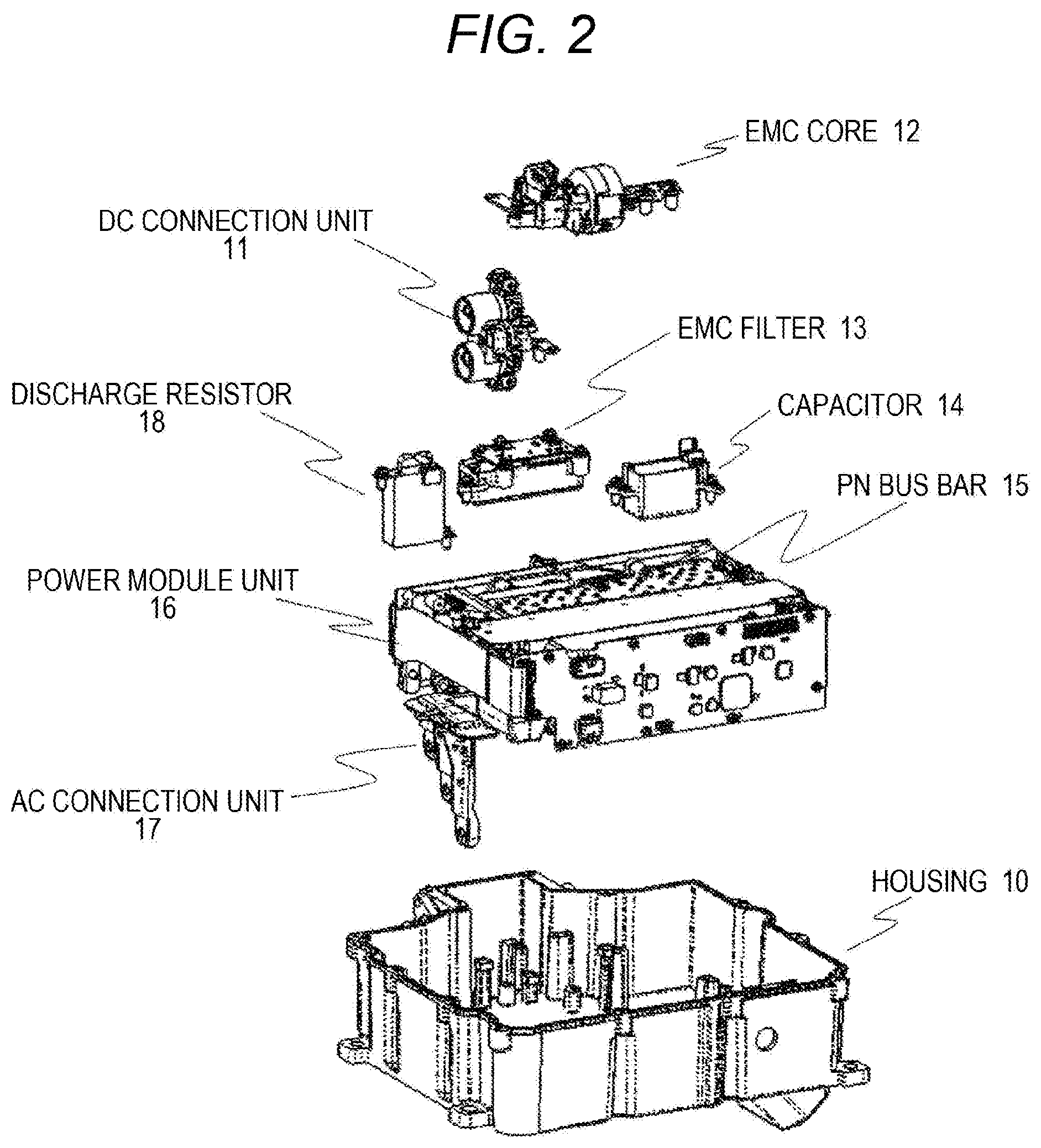
FIG. 2 is a developed view of a power converter 1 according to the present embodiment.
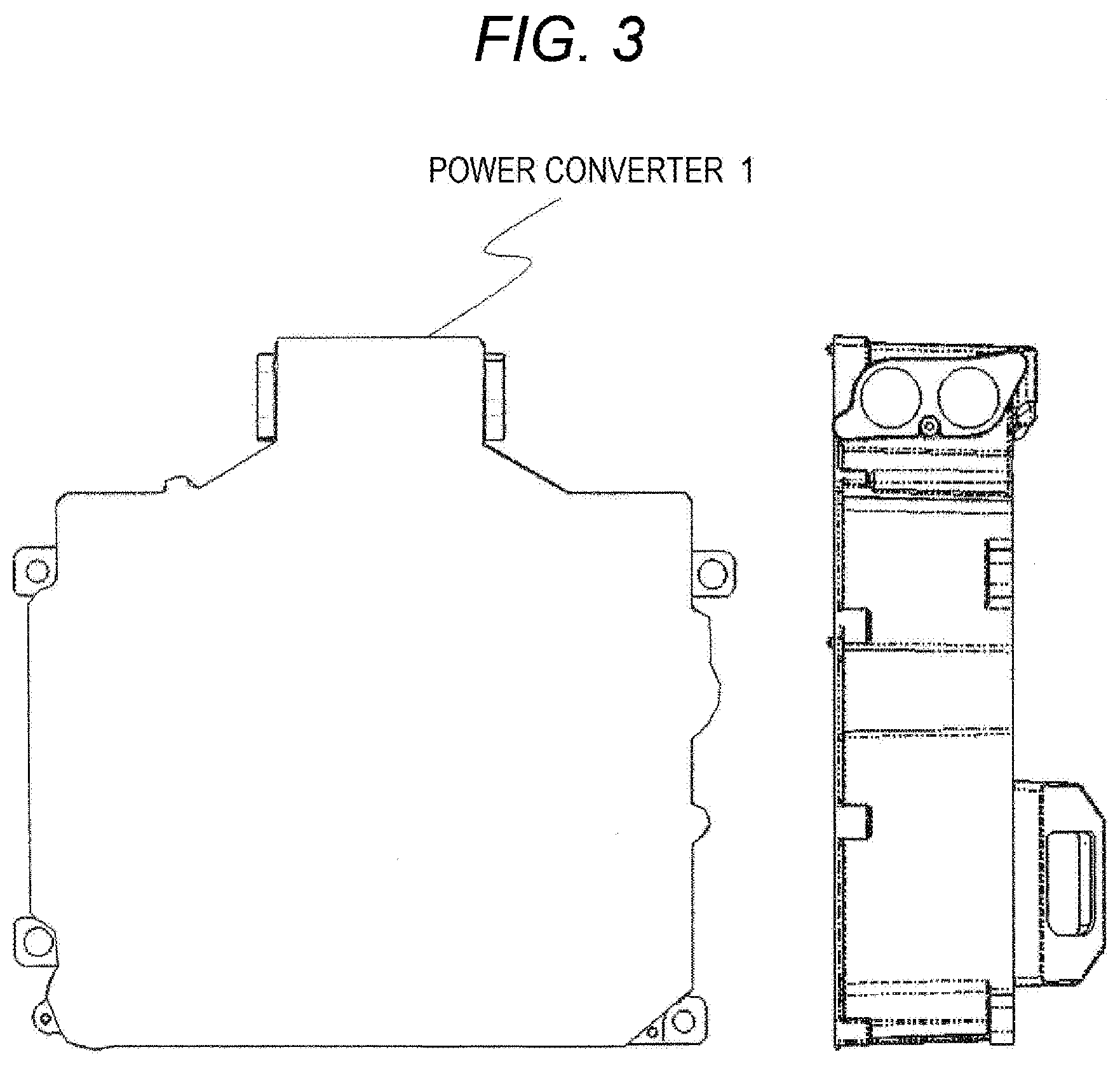
FIG. 3 is an overview of the power converter 1, the left side is a top view and the right side is a side view.
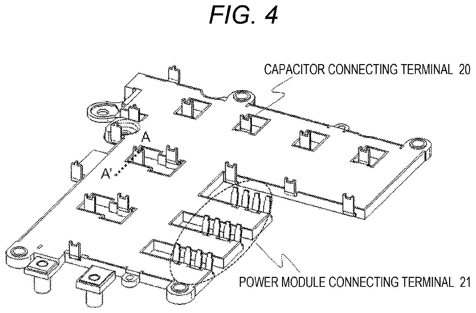
FIG. 4 is an external perspective view of the PN bus bar 15.
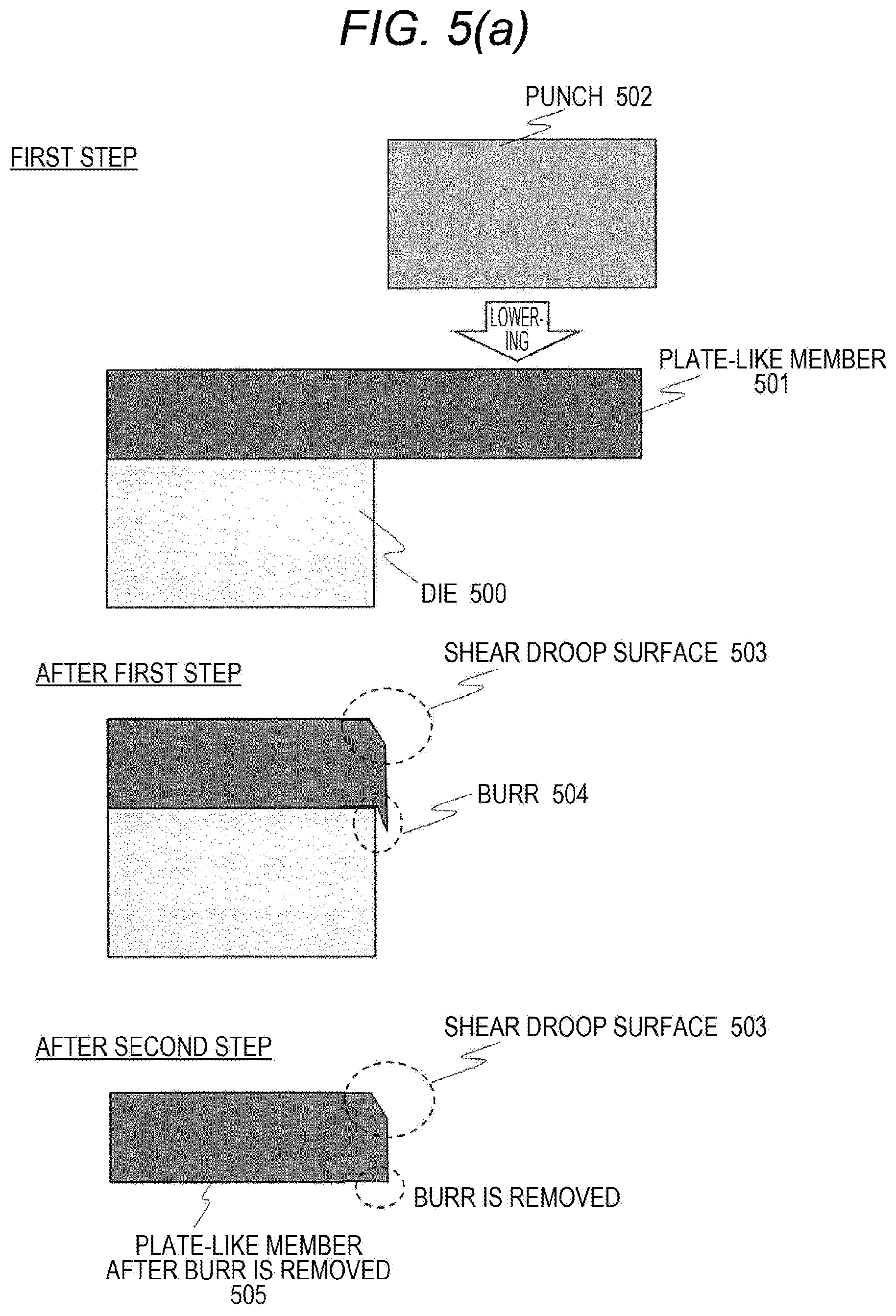
FIG. 5(a) is a conceptual diagram showing an example of a manufacturing step of the PN bus bar 15.
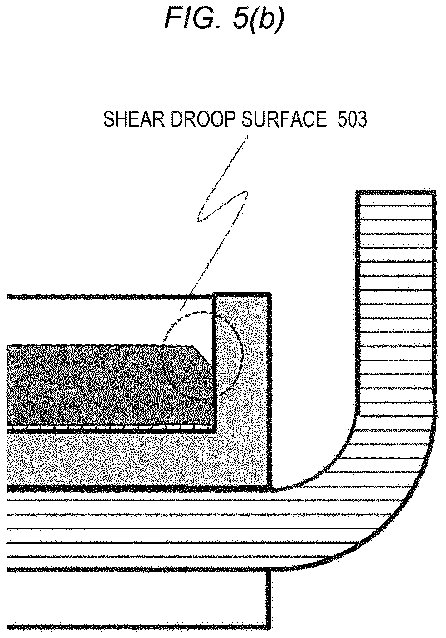
FIG. 5(b) is a conceptual view showing the completion of the PN bus bar 15 created by the manufacturing step of FIG. 5(a).
DESCRIPTION OF EMBODIMENTS
An embodiment according to the present invention will be described with reference to FIGS. 1 to 5(b).
FIG. 2 is a developed view of a power converter according to the present embodiment. FIG. 3 is an overview of the power converter 1, the left side is a top view and the right side is a side view.
A housing 10 accommodates internal components of the power converter 1. A direct current (DC) connection unit inputs and outputs DC power to and from the power converter. An ENC core 12 and an EMC filter 13 suppress electromagnetic noise generated by internal components of the power converter 1.
A power module unit 16 accommodates a semiconductor for converting electric power. The capacitor 14 smoothes electric power when the power module unit 16 converts electric power. A positive negative (PN) bus bar 15 connects a smoothing capacitor and a power module.
An AC connection unit 17 inputs and outputs AC power to and from the power converter. A discharge resistor 18 quickly reduces the voltage when operation of the power converter 1 stops.
FIG. 4 is an external perspective view of the PN bus bar 15.
The PN bus bar 15 includes a positive electrode side conductor 100 and a negative electrode side conductor 101 described later. A capacitor connecting terminal 20 connects the capacitor 14 to the positive electrode side conductor 100 and the negative electrode side conductor 101.
A power module connecting terminal 21 connects the power module unit 16 to the positive electrode side conductor 100 and the negative electrode side conductor 101.
The right side of FIG. 1 is a cross-sectional view of the PN bus bar 15 taken along the line A-A in FIG. 4, and the left side is a cross-sectional view when a through hole 301 is formed in the PN bus bar 15.
The positive electrode side conductor 100 is applied with a positive side DC voltage, and is connected to a positive electrode terminal of the capacitor 14 and a positive electrode terminal of the power module unit 16. The negative electrode side conductor 101 is applied with a negative side DC voltage, and is connected to a negative electrode terminal of the capacitor 14 and a negative electrode terminal of the power module unit 16.
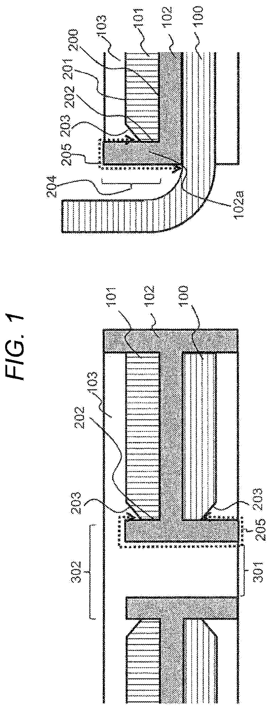
An insulating member 102 is disposed between the positive electrode side conductor 100 and the negative electrode side conductor 101 to insulate between the positive side DC voltage and the negative side DC voltage. The insulating member 102 forms a wall 102a facing a side surface of the negative electrode side conductor 101.
The negative electrode side conductor 101 includes a contact surface 200 in contact with the insulating member 102, a main surface 201 opposite to the contact surface 200, a side surface 202 facing a protrusion 204, and an inclined surface 203 forming an obtuse angle with respect each of the main surface 201 and the side surface 202.
The protrusion 204 of the insulating member 102 is formed so as to overlap with the side surface 202 and the inclined surface 203 when viewed from a direction perpendicular to the side surface 202.
As a result, since the negative electrode side conductor 100 in contact with the insulating member 102 having the protrusion 204 has the inclined surface 203, the creepage distance can be extended as compared with the case where the inclined surface 203 is not provided, and high reliability for creeping discharge can be obtained. Therefore, since the creepage distance can be extended, high insulation reliability can be secured without increasing size.
A sealing resin material 103 filled between at least the inclined surface 203 and the protrusion 204.
The creepage distance 205 is defined by the distance of the shortest path between contact points with the insulating member 102 of the positive electrode side conductor 100 and the negative electrode side conductor 101 on the insulating member 102. Taking the variations in the adhesion state between the sealing resin material 103 and the insulating member 102 into consideration, the space between the sealing resin material 103 and the insulating member 102 in the shortest path between the positive electrode side conductor 100 and the negative electrode side conductor 103 may not be completely adhered, so that the interface is regarded as the contact surface between insulating materials, that is, the creeping surface.
By providing the sealing resin material 103, it is possible to ignore the space distance between the negative electrode side conductor 101 and the insulating member 102, which exists when the sealing resin material 103 is not provided. The space distance is a distance for a space not through the insulating member and is basically different from the creepage distance. However, the space distance less than the prescribed distance according to the pollution degree of the environment treated as a creepage distance. In this case, the space distance is regarded as a creepage distance shorter than the creepage distance 205 taking a path on the insulating member 102. By providing the sealing resin 103, it is unnecessary to consider the space distance, so that even if the pollution degree is high, it is possible to reliably secure the creepage distance.
Since the negative electrode side conductor 101 in contact with the insulating member 102 having the protrusion 204 has the inclined surface 203, the creepage distance can be extended as compared with the case where the inclined surface 203 is not provided, and high reliability for creeping discharge can be obtained. Therefore, it is possible to obtain high insulation reliability against creeping discharge even in an environment with a high pollution degree.
In the left side of FIG. 1, the insulating member 102 has a cylindrical portion 302 forming the through hole 301, and the sealing resin material 103 seals the positive electrode side conductor 100, the negative electrode side conductor 101, and the insulating member 102, and is filled in the through hole 301.
The cylindrical portion 302 is formed so as to overlap with the side surface 202 and the inclined surface 203 when viewed from a direction perpendicular to the side surface 202.
By forming the inclined surface on the negative electrode side conductor 101 of the cylindrical portion 302 which is a structure for filling the sealing resin, the width of the protrusion of the insulating member 102 can be reduced for the amount of the increased creepage distance, and accordingly, the through hole of the conductor can be reduced so that conduction heat generation of the bus bar can be suppressed. As a result, it is possible to use a low-cost member having low heat resistance temperature, or to improve the output of the power converter.
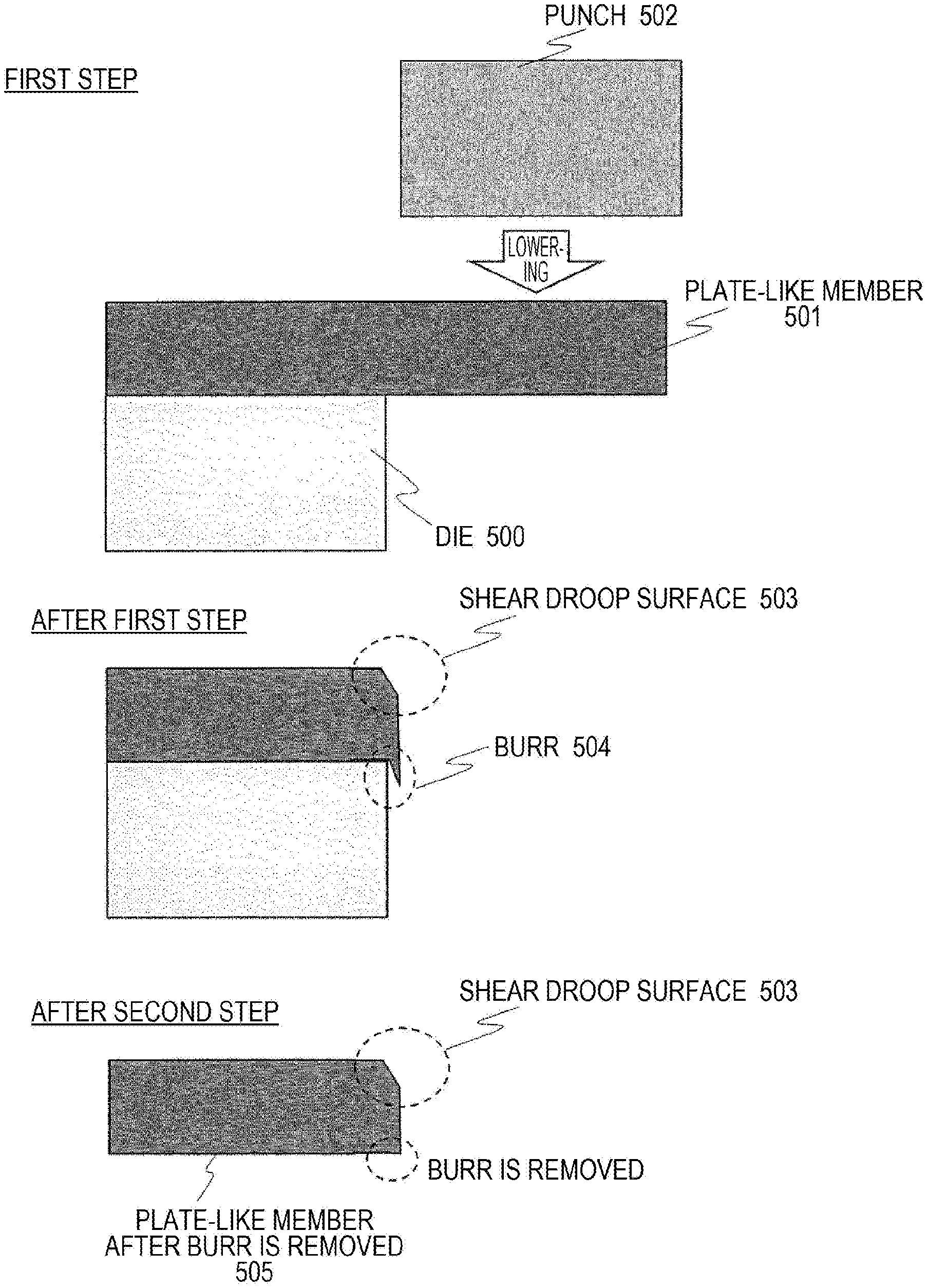
FIG. 5(a) is a conceptual diagram showing an example of a manufacturing step of the PN bus bar 15. FIG. 5(b) is a conceptual view showing the completion of the PN bus bar 15 created by the manufacturing step of FIG. 5(a).
In a first step of FIG. 5(a), a die 500 is a support of a plate-like member 501 to be cut. A punch 503 is a member for lowering the punch 503 and shearing the plate-like member 501.
As shown after the first step of FIG. 5(a), a shear droop surface 503 is an inclined surface formed by deformation of the plate-like member 501 by a downward stress at the time of shearing. Similarly, a burr 504 is a sharp edge portion formed by deformation at the time of shearing.
In a second step of FIG. 5(a), the burr 504 is cut and removed to form the plate-like member 505 after the burr is removed.
In FIG. 5(b), the shear droop surface 503 of the plate-like member 505 after the burr is removed is disposed so as to face the protrusion 204 of the insulating member 102 in FIG. 1. The concrete configuration is such that the inclined surface 203 and the shear droop surface 503 in FIG. 1 are disposed by being regarded as equivalent.
Generally, in order to avoid damage of the insulating member 102 by the burr 504, the shear droop surface 503 is disposed so as to be in contact with the insulating member 102 on the surface in contact with the insulating member 102.
On the other hand, in the present embodiment, the shear droop surface 503 generated during the step is used as the inclined surface 203. For this reason, the burr 504 is removed to obtain a surface in contact with the insulating member 102.
Since this step makes the process of forming the inclined surface 203 unnecessary, an inexpensive power converter can be provided.
In the present embodiment, the shear droop surface 503 in the first step is utilized as the inclined surface 203. However, when an inclined surface is formed in another different step, the surface can of course be used.
Also, as a method of removing the burr 205, cutting removal is taken as an example, but other methods may of course be adopted as long as the burr can be removed.
REFERENCE SIGNS LIST
1 power converter 10 housing 11 DC connection unit 12 EMC core 13 ENC filter 14 capacitor 15 PN bus bar 16 power module unit 17 AC connection unit 18 discharge resistor 20 capacitor connecting terminal 21 power module connecting terminal 100 positive electrode side conductor 101 negative electrode side conductor 102 insulating member 200 contact surface 201 main surface 202 side surface 203 inclined surface 204 protrusion 301 through hole 302 cylindrical portion 500 die 501 plate-like member 503 punch 504 burr 505 plate-like member
* * * * *
D00000
D00001
D00002
D00003
D00004
D00005
D00006
XML
uspto.report is an independent third-party trademark research tool that is not affiliated, endorsed, or sponsored by the United States Patent and Trademark Office (USPTO) or any other governmental organization. The information provided by uspto.report is based on publicly available data at the time of writing and is intended for informational purposes only.
While we strive to provide accurate and up-to-date information, we do not guarantee the accuracy, completeness, reliability, or suitability of the information displayed on this site. The use of this site is at your own risk. Any reliance you place on such information is therefore strictly at your own risk.
All official trademark data, including owner information, should be verified by visiting the official USPTO website at www.uspto.gov. This site is not intended to replace professional legal advice and should not be used as a substitute for consulting with a legal professional who is knowledgeable about trademark law.