Magnetic head with current assisted magnetic recording and method of making thereof
Chembrolu , et al. January 12, 2
U.S. patent number 10,891,974 [Application Number 16/000,033] was granted by the patent office on 2021-01-12 for magnetic head with current assisted magnetic recording and method of making thereof. This patent grant is currently assigned to SANDISK TECHNOLOGIES LLC. The grantee listed for this patent is SANDISK TECHNOLOGIES LLC. Invention is credited to Zhigang Bai, Venkatesh Chembrolu, Lijie Guan, Michael Ho, Terence Lam, Supradeep Narayana, Changqing Shi, Suping Song, Yaguang Wei, Anna Zheng, Jian-Gang Zhu.


View All Diagrams
| United States Patent | 10,891,974 |
| Chembrolu , et al. | January 12, 2021 |
Magnetic head with current assisted magnetic recording and method of making thereof
Abstract
A magnetic head includes a main pole configured to serve as a first electrode, an upper pole containing a trailing magnetic shield configured to a serve as a second electrode, and a record element located in a trailing gap between the main pole and the trailing magnetic shield. The record element includes an electrically conductive, non-magnetic material portion which is not part of a spin torque oscillator stack. The main pole and the trailing magnetic shield are electrically shorted by the record element across the trailing gap between the main pole and the trailing magnetic shield such that an electrically conductive path is present between the main pole and the trailing magnetic shield through the record element.
| Inventors: | Chembrolu; Venkatesh (San Jose, CA), Bai; Zhigang (Fremont, CA), Wei; Yaguang (San Jose, CA), Zheng; Anna (San Ramon, CA), Narayana; Supradeep (San Jose, CA), Song; Suping (Fremont, CA), Lam; Terence (San Jose, CA), Ho; Michael (San Jose, CA), Shi; Changqing (San Ramon, CA), Guan; Lijie (Cupertino, CA), Zhu; Jian-Gang (San Jose, CA) | ||||||||||
|---|---|---|---|---|---|---|---|---|---|---|---|
| Applicant: |
|
||||||||||
| Assignee: | SANDISK TECHNOLOGIES LLC
(Addison, TX) |
||||||||||
| Family ID: | 1000003813822 | ||||||||||
| Appl. No.: | 16/000,033 | ||||||||||
| Filed: | June 5, 2018 |
Related U.S. Patent Documents
| Application Number | Filing Date | Patent Number | Issue Date | ||
|---|---|---|---|---|---|
| 62497299 | Jun 7, 2017 | ||||
| Current U.S. Class: | 1/1 |
| Current CPC Class: | G11B 5/315 (20130101); G11B 5/23 (20130101); G11B 5/3133 (20130101); G11B 5/1278 (20130101); G11B 5/115 (20130101); G11B 5/3146 (20130101); G11B 5/187 (20130101) |
| Current International Class: | G11B 5/31 (20060101); G11B 5/23 (20060101); G11B 5/115 (20060101); G11B 5/187 (20060101); G11B 5/127 (20060101) |
| Field of Search: | ;360/119.02,119.04,125.3 |
References Cited [Referenced By]
U.S. Patent Documents
| 4822159 | April 1989 | Gaiser |
| 4881143 | November 1989 | Bhattacharyya |
| 5784224 | July 1998 | Rottmayer |
| 6493183 | December 2002 | Kasiraj |
| 6636393 | October 2003 | Araki et al. |
| 6661623 | December 2003 | Tsuchiya et al. |
| 6820022 | November 2004 | Carbone, II et al. |
| 7072142 | July 2006 | Lam |
| 7397633 | July 2008 | Xue et al. |
| 7983002 | July 2011 | Pust et al. |
| 8107352 | January 2012 | Yamanaka et al. |
| 8116031 | February 2012 | Alex et al. |
| 8159781 | April 2012 | Taguchi et al. |
| 8189292 | May 2012 | Pentek et al. |
| 8194361 | June 2012 | Kudo et al. |
| 8238059 | August 2012 | Tang et al. |
| 8339736 | December 2012 | Gao et al. |
| 8355222 | January 2013 | Mino et al. |
| 8390955 | March 2013 | Sasaki et al. |
| 8404128 | March 2013 | Zhang |
| 8405930 | March 2013 | Li et al. |
| 8422159 | April 2013 | Gao et al. |
| 8456967 | June 2013 | Mallary |
| 8472135 | June 2013 | Kusukawa et al. |
| 8508984 | August 2013 | Ranjan et al. |
| 8547661 | October 2013 | Bai |
| 8553362 | October 2013 | Tanabe et al. |
| 8582240 | November 2013 | Chen et al. |
| 8634163 | January 2014 | Tanabe et al. |
| 8767346 | July 2014 | Yamada et al. |
| 8786984 | July 2014 | Das et al. |
| 8810961 | August 2014 | Taguchi et al. |
| 8837088 | September 2014 | Kimura et al. |
| 8908330 | December 2014 | Mallary |
| 8929030 | January 2015 | Hou et al. |
| 8930955 | January 2015 | Baset et al. |
| 8988826 | March 2015 | Sugiyama et al. |
| 8995088 | March 2015 | Boone |
| 9042151 | May 2015 | Annunziata et al. |
| 9047887 | June 2015 | Funayama |
| 9099102 | August 2015 | Katada et al. |
| 9129621 | September 2015 | Kimura et al. |
| 9142227 | September 2015 | Etoh et al. |
| 9230568 | January 2016 | Ikegawa |
| 9230571 | January 2016 | Chen et al. |
| 9230573 | January 2016 | Etoh et al. |
| 9275672 | March 2016 | Shiroishi et al. |
| 9286916 | March 2016 | Rivkin et al. |
| 9311934 | April 2016 | Shiimoto et al. |
| 9368135 | June 2016 | Gao |
| 9390733 | July 2016 | Etoh et al. |
| 9406316 | August 2016 | Urakami et al. |
| 9449621 | September 2016 | Mauri et al. |
| 9551637 | January 2017 | Fox et al. |
| 9589581 | March 2017 | Takagishi et al. |
| 9640203 | May 2017 | Buch et al. |
| 9640206 | May 2017 | Saito et al. |
| 9691415 | June 2017 | Koui |
| 9747932 | August 2017 | Taguchi et al. |
| 9870786 | January 2018 | Funayama et al. |
| 9881637 | January 2018 | Wilson et al. |
| 10014012 | July 2018 | Song et al. |
| 10121497 | November 2018 | Takahashi et al. |
| 10186284 | January 2019 | Narita et al. |
| 10210888 | February 2019 | Li et al. |
| 10236021 | March 2019 | Narita et al. |
| 10276193 | April 2019 | Narita et al. |
| 10325618 | June 2019 | Wu et al. |
| 10366714 | July 2019 | Olson et al. |
| 2001/0020884 | September 2001 | Araki |
| 2003/0112555 | June 2003 | Sato et al. |
| 2004/0145850 | July 2004 | Fukumoto et al. |
| 2005/0058855 | March 2005 | Girt |
| 2005/0128637 | June 2005 | Johnston et al. |
| 2005/0219748 | October 2005 | Guthrie |
| 2006/0067016 | March 2006 | Childress et al. |
| 2006/0215315 | September 2006 | Miyake et al. |
| 2007/0121249 | May 2007 | Parker |
| 2007/0297081 | December 2007 | Nazarov et al. |
| 2008/0112087 | May 2008 | Clinton et al. |
| 2008/0268291 | October 2008 | Akiyama |
| 2008/0304176 | December 2008 | Takagishi et al. |
| 2009/0009907 | January 2009 | Zhang |
| 2009/0016266 | January 2009 | Kim et al. |
| 2009/0059423 | March 2009 | Yamada et al. |
| 2009/0080120 | March 2009 | Funayama et al. |
| 2009/0168266 | July 2009 | Sato et al. |
| 2009/0262636 | October 2009 | Xue et al. |
| 2009/0310244 | December 2009 | Shimazawa et al. |
| 2010/0290156 | November 2010 | Anderson |
| 2010/0315747 | December 2010 | Matsumoto et al. |
| 2011/0090584 | April 2011 | Franca-Neto et al. |
| 2011/0216432 | September 2011 | Yanagisawa |
| 2011/0216435 | September 2011 | Shiimoto et al. |
| 2011/0293967 | December 2011 | Zhang et al. |
| 2012/0044598 | February 2012 | Bai |
| 2012/0147502 | June 2012 | Udo et al. |
| 2013/0050875 | February 2013 | Yamada |
| 2013/0063837 | March 2013 | Udo et al. |
| 2013/0146997 | June 2013 | Lee et al. |
| 2013/0149499 | June 2013 | Lee et al. |
| 2013/0250456 | September 2013 | Yamada et al. |
| 2013/0251042 | September 2013 | Lee |
| 2013/0271869 | October 2013 | Taguchi et al. |
| 2013/0336045 | December 2013 | Kuo et al. |
| 2014/0044598 | February 2014 | Hu et al. |
| 2014/0078618 | March 2014 | Matsumoto et al. |
| 2014/0139952 | May 2014 | Takeo et al. |
| 2014/0146420 | May 2014 | Shimizu et al. |
| 2014/0175050 | June 2014 | Zhang et al. |
| 2014/0175575 | June 2014 | Doyle et al. |
| 2014/0177100 | June 2014 | Sugiyama |
| 2015/0029615 | January 2015 | Chembrolu |
| 2015/0098150 | April 2015 | Chiu et al. |
| 2015/0103434 | April 2015 | Etoh et al. |
| 2015/0103437 | April 2015 | Watanabe et al. |
| 2015/0126326 | May 2015 | Kobayashi et al. |
| 2015/0154987 | June 2015 | Etoh et al. |
| 2015/0213814 | July 2015 | Chembrolu et al. |
| 2015/0213820 | July 2015 | Chembrolu et al. |
| 2015/0380017 | December 2015 | Chembrolu et al. |
| 2016/0024755 | January 2016 | Kobiki |
| 2016/0027455 | January 2016 | Kudo et al. |
| 2016/0035375 | February 2016 | Gao |
| 2016/0148629 | May 2016 | Gao et al. |
| 2016/0225392 | August 2016 | Takeo et al. |
| 2016/0300999 | October 2016 | Yi et al. |
| 2016/0343391 | November 2016 | Sasaki et al. |
| 2017/0018285 | January 2017 | Chen et al. |
| 2017/0061995 | March 2017 | Taguchi et al. |
| 2017/0104151 | April 2017 | Banerjee et al. |
| 2017/0140779 | May 2017 | Koui |
| 2017/0148471 | May 2017 | Tabata et al. |
| 2017/0148474 | May 2017 | Okamura et al. |
| 2017/0236537 | August 2017 | Murakami et al. |
| 2017/0309301 | October 2017 | Takahashi et al. |
| 2018/0247668 | August 2018 | Biskeborn |
| 2018/0266848 | September 2018 | Das et al. |
| 2018/0268848 | September 2018 | Narita et al. |
| 2019/0088274 | March 2019 | Narita et al. |
| 2019/0180779 | June 2019 | Biskeborn |
| 2019/0251991 | August 2019 | Le et al. |
| 2019/0259413 | August 2019 | Le et al. |
| 2019/0267029 | August 2019 | Bai et al. |
| 2020/0005815 | January 2020 | Bai |
| 2020/0090658 | March 2020 | Shin et al. |
| 2020/0090685 | March 2020 | Takagishi et al. |
| 2020/0152228 | May 2020 | Tang |
| 2020/0294535 | September 2020 | Narita |
| 104835510 | Nov 2017 | CN | |||
| 2013251042 | Dec 2013 | JP | |||
| 2015126326 | Aug 2015 | WO | |||
Other References
|
US. Appl. No. 16/000,103, filed Jun. 5, 2018, Sandisk Technologies LLC. cited by applicant . Mallary, Mike et al; "Head and Media Challenges for 3 Tb/in2 Microwave-Assisted Magnetic Recording"; IEEE Transactions on Magnetics, vol. 50, No. 7, Jul. 2014 (8 pages). cited by applicant . Kanai, Yasushi et al.: "Micromagnetic Model Simulations Considering Write Head, Spin-Torque Oscillator, and Double-Layered Medium Altogether"; Nigata Institute of Technology; IEEE Transactions on Magnetics; Sep. 2018; http://tmrc2018.ucsd.edu/Archive/C2.pdf (2 pages). cited by applicant . Y. Kanai et al.: "Micromagnetic Model Analysis of Various Spin Torque Oscillators with Write Head for Mircowave-assisted Magnetic Recording" IEEE International Magnetics Conference; Dublin, Ireland Apr. 24-28, 2017; https://ieeexplore.ieee.org/document/8007581 (2 pages). cited by applicant . U.S. Appl. No. 16/252,315, filed Jan. 18, 2019. cited by applicant . U.S. Appl. No. 16/998,989, filed Aug. 20, 2020. cited by applicant . U.S. Appl. No. No. 16/000,033, filed Jun. 5, 2018. cited by applicant . U.S. Appl. No. 16/000,103, filed Jun. 5, 2018. cited by applicant. |
Primary Examiner: Evans; Jefferson A
Attorney, Agent or Firm: Patterson & Sheridan, LLP Versteeg; Steven H.
Claims
What is claimed is:
1. A magnetic head, comprising: a main pole configured to serve as a first electrode; an upper pole comprising a trailing magnetic shield configured to a serve as a second electrode; and a record element located in a trailing gap between the main pole and the trailing magnetic shield, the record element comprising an electrically conductive, non-magnetic material portion and a spin torque oscillator stack; wherein the electrically conductive, non-magnetic material portion is not part of the spin torque oscillator stack, wherein the main pole and the trailing magnetic shield are electrically shorted by the record element across the trailing gap between the main pole and the trailing magnetic shield such that an electrically conductive path is present between the main pole and the trailing magnetic shield through the record element, and wherein the electrically conductive path comprises a first electrically conductive path between the first electrode and the second electrode through the spin torque oscillator stack, and a parallel second electrically conductive path between the first electrode and the second electrode through the electrically conductive, non-magnetic material portion.
2. The magnetic head of claim 1, further comprising an electrical bias circuitry configured to flow electrical current between the first electrode and the second electrode through the record element.
3. The magnetic head of claim 2, further comprising: a first electrical contact connecting a portion of the main pole distant from an air bearing surface to the electrical bias circuitry; a second electrical contact connecting a portion of the upper pole distant from the air bearing surface to the electrical bias circuitry; and an electrically insulating material layer located between the portions of the main pole and the upper pole distal from the air bearing surface.
4. The magnetic head of claim 3, wherein: the electrically insulating material layer provides physical and electrical isolation between the portions of the main pole and the upper pole distal from the air bearing surface; and the only electrically conductive path between the main pole and the upper pole is the electrically conductive path between the main pole and the trailing magnetic shield through the record element.
5. The magnetic head of claim 1, wherein: the magnetic head comprises a microwave assisted magnetic recording head; and an air bearing surface (ABS) of the magnetic head includes planar surfaces of the main pole, the spin torque oscillator stack, and the trailing magnetic shield.
6. The magnetic head of claim 5, wherein the electrically conductive, non-magnetic material portion is spaced from the air bearing surface by a portion of the trailing magnetic shield and by the spin torque oscillator stack.
7. The magnetic head of claim 6, wherein the electrically conductive, non-magnetic material portion contacts a leading surface of the trailing magnetic shield.
8. The magnetic head of claim 5, wherein the record element further comprises a conductive layer stack having a same set of component layers as the spin torque oscillator stack, located within the second electrically conductive path, and spaced from the spin torque oscillator stack by a dielectric spacer.
9. The magnetic head of claim 8, wherein: the conductive layer stack and the spin torque oscillator stack are located directly on a trailing sidewall of the main pole; the electrically conductive, non-magnetic material portion comprises a copper layer located on a trailing sidewall of the conductive layer stack; and an interface between the spin torque oscillator stack and the trailing magnetic shield is within a same plane as an interface between the conductive layer stack and the electrically conductive, non-magnetic material portion.
10. The magnetic head of claim 5, further comprising an additional electrically conductive, non-magnetic material portion which is spaced from the air bearing surface by the spin torque oscillator stack.
11. The magnetic head of claim 10, wherein: the additional electrically conductive, non-magnetic material portion contacts a trailing sidewall of the main pole and a rear sidewall of the spin torque oscillator stack that is located on an opposite side of the spin torque oscillator from the air bearing surface; the electrically conductive, non-magnetic material portion is located on a trailing sidewall of the additional electrically conductive, non-magnetic material portion; and an interface between the spin torque oscillator stack and the trailing magnetic shield is within a same plane as an interface between the additional electrically conductive, non-magnetic material portion and the electrically conductive, non-magnetic material portion.
12. The magnetic head of claim 1, further comprising an electrical coil that is located adjacent to the main pole and configured to generate a magnetic flux through the main pole upon conduction of electrical current through the electrical coil.
13. A hard disk drive, comprising: the magnetic head of claim 12; a slider supporting the magnetic head; an actuator arm supporting the slider; a voice coil motor configured to control the actuator arm; and a magnetic disk.
14. A method of operating a magnetic recording head, the method comprising: providing a current between a main pole and an upper pole containing a trailing magnetic shield through a record element located in a trailing gap between the main pole and the trailing shield while applying a magnetic field to the main pole from a coil to record data to a magnetic disk, wherein the record element comprises an electrically conductive, non-magnetic material portion which is not part of a spin torque oscillator stack, wherein the record element further comprises a spin torque oscillator stack, wherein the current flows through a first electrically conductive path which is present between the main pole and the upper pole through the spin torque oscillator stack, and wherein the current flows through a parallel second electrically conductive path which is present between the main pole and the upper pole through the electrically conductive, non-magnetic material portion.
15. The method of claim 14, wherein: the current is provided through a first electrical contact connecting a portion of the main pole distant from an air bearing surface to electrical bias circuitry and a second electrical contact connecting a portion of the upper pole distant from the air bearing surface to the electrical bias circuitry; an electrically insulating material layer is located between the portions of the main pole and the upper pole distal from the air bearing surface; the electrically insulating material layer provides physical and electrical isolation between the portions of the main pole and the upper pole distal from the air bearing surface; and the current flows between the main pole and the upper pole only through the record element.
16. The method of claim 14, wherein: the magnetic head comprises a microwave assisted magnetic recording head; and an air bearing surface (ABS) of the magnetic recording head includes planar surfaces of the main pole, the spin torque oscillator stack, and the trailing magnetic shield which moves over the magnetic disk.
17. A magnetic head, comprising: a main pole configured to serve as a first electrode; an upper pole comprising a trailing magnetic shield configured to a serve as a second electrode; and an electrically conductive, non-magnetic material record element located in a trailing gap between and in contact with the main pole and the trailing magnetic shield; wherein the electrically conductive, non-magnetic material record element is not part of a spin torque oscillator stack, wherein the main pole and the trailing magnetic shield are electrically shorted by the electrically conductive, non-magnetic material record element across the trailing gap between the main pole and the trailing magnetic shield such that an electrically conductive path is present between the main pole and the trailing magnetic shield through the record element, wherein the magnetic head comprises a non-microwave assisted magnetic recording head which lacks a spin torque oscillator stack, wherein the electrically conductive path is present through the electrically conductive, non-magnetic material record element between the first electrode and the second electrode, and wherein the electrically conductive, non-magnetic material record element contacts a trailing sidewall of the main pole and a leading sidewall of the trailing magnetic shield in the trailing gap between the main pole and the trailing magnetic shield.
18. The magnetic head of claim 17, wherein an air bearing surface (ABS) of the magnetic head includes planar surfaces of the main pole, the electrically conductive, non-magnetic material record element, and the trailing magnetic shield.
19. The magnetic head of claim 18, further comprising an insulating material portion recessed from the ABS, the insulating material portion being disposed on the electrically conductive, non-magnetic material record element between and in contact with the main pole and the trailing magnetic shield.
20. The magnetic head of claim 19, wherein a width of the insulating material portion is greater than a width of the electrically conductive, non-magnetic material record element.
21. The magnetic head of claim 17, wherein the only electrically conductive path between the main pole and the upper pole is the electrically conductive path between the main pole and the trailing magnetic shield through the electrically conductive, non-magnetic material record element.
22. The magnetic head of claim 17, wherein the electrically conductive, non-magnetic material record element comprises a copper, gold, platinum, ruthenium, chromium or tungsten layer.
Description
FIELD
The present disclosure relates generally to the field of magnetic recording heads, and particular to current assisted magnetic recording, i.e., magnetic recording heads employing Ampere field enhancement and methods of manufacturing such magnetic recording heads.
BACKGROUND
Disk drives comprise a disk and a head connected to a distal end of an actuator arm which is rotated about a pivot by a voice coil motor (VCM) to position the head radially over the disk. The disk comprises a plurality of radially spaced, concentric tracks for recording user data sectors and servo sectors. The servo sectors comprise head positioning information (e.g., a track address) which is read by the head and processed by a servo control system to control the actuator arm as it seeks from track to track.
FIG. 1 shows a prior art disk 902 comprising a number of servo tracks 904 defined by servo sectors 906.sub.0-906.sub.N recorded around the circumference of each servo track. Each servo sector 906.sub.i comprises a preamble 908 for storing a periodic pattern, which allows proper gain adjustment and timing synchronization of the read signal, and a sync mark 910 for storing a special pattern used to symbol synchronize to a servo data field 912. The servo data field 912 stores coarse head positioning information, such as a servo track address, used to position the head over a target data track during a seek operation. Each servo sector 906.sub.i further comprises groups of servo bursts 914 (e.g., N and Q servo bursts), which are recorded with a predetermined phase relative to one another and relative to the servo track centerlines. The phase based servo bursts 914 provide fine head position information used for centerline tracking while accessing a data track during write/read operations. A position error signal (PES) is generated by reading the servo bursts 914, wherein the PES represents a measured position of the head relative to a centerline of a target servo track. A servo controller processes the PES to generate a control signal applied to a head actuator (e.g., a voice coil motor) in order to actuate the head radially over the disk in a direction that reduces the PES.
FIG. 2A illustrates a conventional disk drive 810 used for data storage. A disk media (i.e., a magnetic disk) 850 is attached to a spindle motor and hub 820. The spindle motor and hub 820 rotate the media 850 in a direction shown by arrow 855. A head stack assembly (HSA) 815 includes a carriage 820 and a voice coil motor (VCM) 825. A first end of an actuator arm 870 is supported by the carriage 820. A second end of the actuator arm 870 supports a head-gimbal assembly (HGA) 830. The HSA 815 positions the actuator arm 870 using the voice coil motor (VCM) 825 and a pivot shaft and bearing assembly 860 over a desired data track 840 of the disk media 850 to read and/or write data from and/or to the data track 840.
FIG. 2B illustrates the details of the HGA 830 located over the data track 840. The HGA 830 includes a slider 880 located above the data track 840 and a magnetic head 600 (also called a recording head or a reading and recording head) located on the slider 880. The magnetic head 600 contains a recording head (also called a magnetic recording transducer, a writing head or a writer) 660. The magnetic head 600 may also contain a reading head (also called a magnetic reading transducer, a reading element or a reader) 610. The media 850 and the track 840 move under the slider 880 in a down-track direction shown by arrow 842. The cross-track direction is shown by arrow 841. The recording head 660 has a leading edge 891 and a trailing edge 892. In this embodiment, the trailing edge 892 of the recording head 660 is the final portion of the recording head 660 that writes (i.e., records) data onto the data track 840 as the media 850 moves under the slider 880 in the down-track direction 842.
FIG. 3 illustrates a side view of the disk drive 810 shown in FIG. 2A. At least one disk media 850 (e.g., plural disk media 850) are mounted onto the spindle motor and hub 820. The HSA 815 supports at least one actuator arm 870 (e.g., plural arms 870). Each actuator arm 870 carries a suspension 875 and the slider 880. The slider 880 has an air bearing surface (ABS) facing the media 850. When the media 850 is rotating and the actuator arm 870 is positioned over the media 850, the slider 880 slides above the media 850 by aerodynamic pressure created between the slider ABS and the surface of media 850.
Data is typically written to the disk by modulating a write current in an inductive coil to record magnetic transitions onto the disk surface in a process referred to as saturation recording. During readback, the magnetic transitions are sensed by a read head and the resulting read signal demodulated by a suitable read channel. However, as conventional perpendicular magnetic recording (PMR) approaches its limit, further growth of the areal recording density becomes increasingly challenging.
SUMMARY
According to an aspect of the present disclosure, a magnetic head includes a main pole configured to serve as a first electrode, an upper pole containing a trailing magnetic shield configured to a serve as a second electrode, and a record element located in a trailing gap between the main pole and the trailing magnetic shield. The record element includes an electrically conductive, non-magnetic material portion which is not part of a spin torque oscillator stack. The main pole and the trailing magnetic shield are electrically shorted by the record element across the trailing gap between the main pole and the trailing magnetic shield such that an electrically conductive path is present between the main pole and the trailing magnetic shield through the record element.
According to another aspect of the present disclosure, a method of operating a magnetic recording head comprising providing a current between a main pole and an upper pole containing a trailing magnetic shield through a record element located in a trailing gap between the main pole and the trailing shield while applying a magnetic field to the main pole from a coil to record data to a magnetic disk. The record element comprises an electrically conductive, non-magnetic material portion which is not part of a spin torque oscillator stack.
According to yet another aspect of the present disclosure, method of forming a magnetic head comprises forming a main pole over a substrate, forming an electrically conductive, non-magnetic material portion over the main pole, forming a trailing magnetic shield directly on a trailing sidewall of the electrically conductive, non-magnetic material portion, and forming an air bearing surface (ABS) of the magnetic head by lapping portions of the main pole and the trailing magnetic shield. An electrically conductive path is present between the main pole and the trailing magnetic shield through the electrically conductive, non-magnetic material portion.
BRIEF DESCRIPTION OF THE DRAWINGS
FIG. 1 shows a top view of prior art disk including a plurality of servo tracks defined by servo sectors.
FIG. 2A illustrates a top view of a conventional hard disk drive and FIG. 2B schematically illustrates a top view of a head-gimbal assembly of the hard disk drive of FIG. 2A.
FIG. 3 illustrates a side view of the conventional hard disk drive of FIG. 2A.
FIG. 4 is an in-track vertical cross-sectional view of an exemplary magnetic head of the present disclosure.
FIG. 5A is an in-track vertical cross-sectional view of a first exemplary recording head according to a first embodiment of the present disclosure.
FIG. 5B is an air bearing surface (ABS) view of a portion of the first exemplary recording head according to the first embodiment of the present disclosure.
FIG. 6 is an in-track vertical cross-sectional view of a second exemplary recording head according to a second embodiment of the present disclosure.
FIG. 7A is an in-track vertical cross-sectional view of a third exemplary recording head according to a third embodiment of the present disclosure.
FIG. 7B is an ABS view of a portion of the third exemplary recording head according to the third embodiment of the present disclosure.
FIGS. 8A-8F are sequential vertical cross-sectional views of a first exemplary structure for manufacture of the first exemplary recording head according to the first embodiment of the present disclosure.
FIGS. 9A-9E are sequential vertical cross-sectional views of a second exemplary structure for manufacture of the second exemplary recording head according to the second embodiment of the present disclosure.
FIGS. 10A-10C are sequential vertical cross-sectional views of a third exemplary structure for manufacture of the third exemplary recording head according to the third embodiment of the present disclosure.
FIG. 11 shows magnetization M, bias current I, and the current induced Ampere's field in the main pole and in the trailing shield in the vicinity of a trailing gap according to an embodiment of the present disclosure.
FIG. 12 shows finite element model (FEM) simulation results of the bias current distribution and the Ampere's field (MP) produced by 5 mA of the bias current through the main pole according to an embodiment of the present disclosure.
DETAILED DESCRIPTION
As discussed above, the present disclosure is directed to magnetic recording heads employing Ampere field enhancement and methods of manufacturing such magnetic recording heads.
The drawings are not drawn to scale. Multiple instances of an element may be duplicated where a single instance of the element is illustrated, unless absence of duplication of elements is expressly described or clearly indicated otherwise. Ordinals such as "first," "second," and "third" are employed merely to identify similar elements, and different ordinals may be employed across the specification and the claims of the instant disclosure. The same reference numerals refer to the same element or similar element. Unless otherwise indicated, elements having the same reference numerals are presumed to have the same composition. As used herein, a first element located "on" a second element can be located on the exterior side of a surface of the second element or on the interior side of the second element. As used herein, a first element is located "directly on" a second element if there exist a physical contact between a surface of the first element and a surface of the second element.
As used herein, a "layer" refers to a material portion including a region having a thickness. A layer may extend over the entirety of an underlying or overlying structure, or may have an extent less than the extent of an underlying or overlying structure. Further, a layer may be a region of a homogeneous or inhomogeneous continuous structure that has a thickness less than the thickness of the continuous structure. For example, a layer may be located between any pair of horizontal planes between, or at, a top surface and a bottom surface of the continuous structure. A layer may extend horizontally, vertically, and/or along a tapered surface. A substrate may be a layer, may include one or more layers therein, or may have one or more layer thereupon, thereabove, and/or therebelow.
As used herein, an "electrically conductive material" refers to a material having electrical conductivity greater than 1.0.times.10.sup.5 S/cm. As used herein, a "metallic material" refers to a conductive material including at least one metallic element therein. As used herein, an "electrically insulating material" or a "dielectric material" refers to a material having electrical conductivity less than 1.0.times.10.sup.-6 S/cm. As used herein, a "semiconducting material" refers to a material having electrical conductivity in the range from 1.0.times.10.sup.-6 S/cm to 1.0.times.10.sup.5 S/cm. All measurements for electrical conductivities are made at the standard condition.
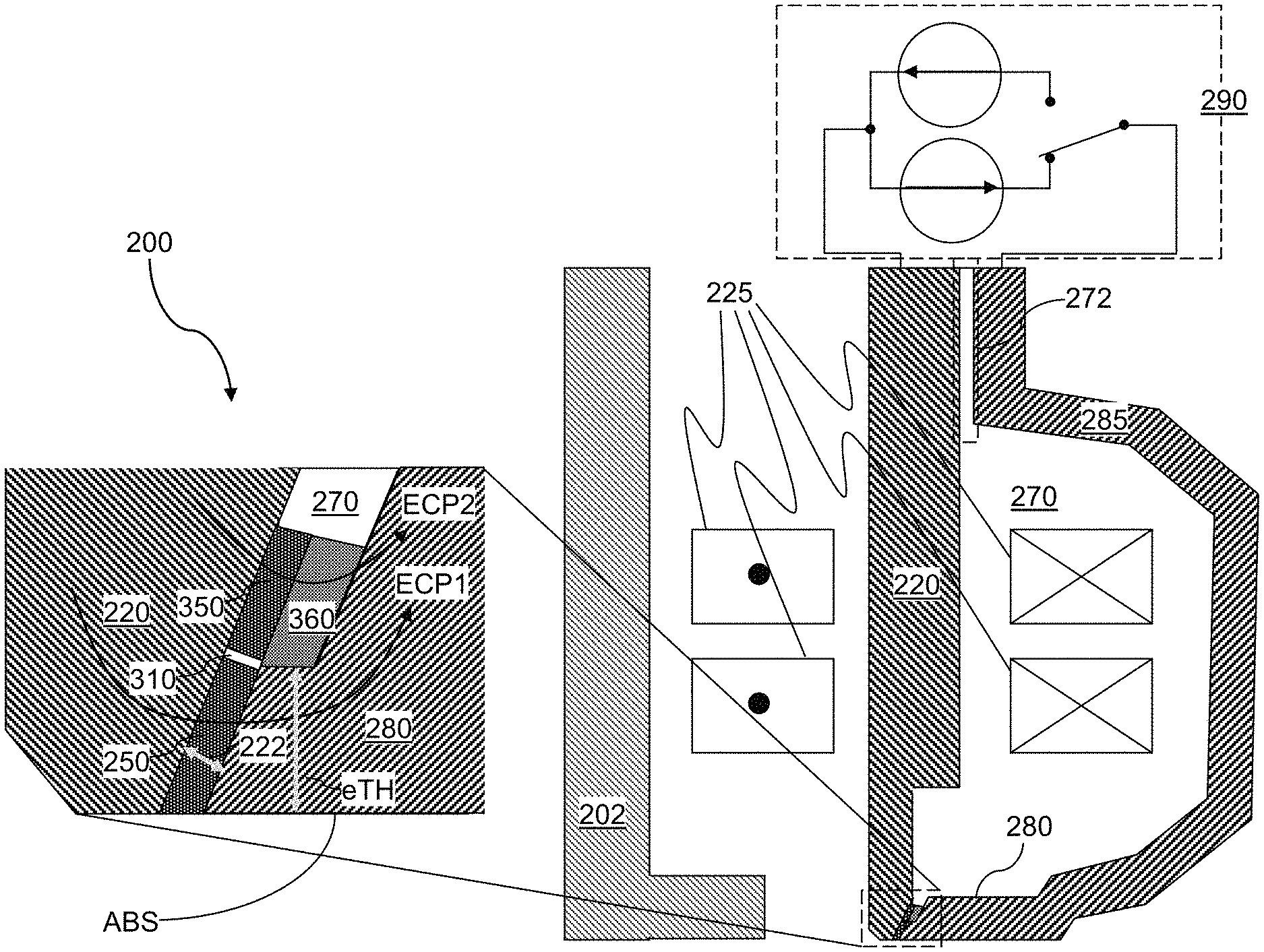
Referring to FIG. 4, an in-track vertical cross-sectional view of an exemplary magnetic head 600 of one embodiment of the present disclosure is illustrated. The magnetic head 600 is configured for microwave assisted magnetic recording (MAMR) employing a microwave generating spin torque oscillator (STO). The magnetic head 600 is positioned over a recording track 840 on a disk media. The magnetic head 600 comprises, from the leading side of the head (i.e., the left side of FIG. 4), a reading head 610 and a recording head 660. The reading head comprises a lower reading shield 620, a read sensor 650 (i.e., a reading element), and an upper reading shield 690. The read sensor 650 can include a tunnel magnetoresistance (TMR) device, a giant magnetoresistance (GMR) device, or the like.
The recording head 660 can comprise a record element 200 that includes a microwave-generating spin torque oscillator (STO) element, an optional auxiliary pole 202, a main pole 220, a magnetic coil 225 that is wound around the main pole 220, and a trailing shield 280 which may be integrated with an upper pole 285. The record element 200 is formed in a gap between the main pole 220 and the trailing shield 280. The main pole 220 and trailing shield 280 serve as first and second electrodes for flowing electrical current through the record element 200 during recording (i.e., writing). A bias circuitry 290 can be electrically connected to the main pole 220 and the upper pole 285, such as to the end portions of the main pole and the upper pole 285 distal from the ABS and the record element 200. The bias circuitry 290 may include a voltage or current source (or a connection to an external voltage or current source) and one or more switching devices, such as transistors or relays which can switch the voltage or current on and off. The bias circuitry 290 is configured to provide a current or voltage to the main pole 220 and the upper pole 285. For example, the bias circuitry 290 may provide a current between the main pole 220 and the upper pole 285/trailing shield 280 that flows through the record element 200. An insulating material portion 270 is provided around the magnetic coil 225 between the main pole 220, the trailing shield 280 and the upper pole 285. An electrically insulating material layer 272 can be provided between end portions of the main pole 220 and the upper pole 285 where the bias circuitry connections (i.e., electrical contacts 291, 292 attached to the ends of the main pole and upper pole respectively) are made (i.e., distal from the ABS).
During operation of the recording head 660, if perpendicular magnetic recording is employed, a magnetic field emitted from the main pole 220 passes through a magnetic recording layer (e.g., hard magnetic layer) 710 and a soft magnetic underlayer 720 of the recording track 840 of the disk media 850, and returns to the auxiliary pole 202. A magnetization pattern (represented by arrows) is recorded in the magnetic recording layer 710. In a MAMR system, the magnetization pattern is recorded when electrical current flows between the main pole 210 and the upper pole 285 which is physically and electrically connected to trailing shield 280, and a high-frequency magnetic field from the STO element of the record element 200 is applied to the recording track 840 to temporarily reduce the coercivity of the magnetic recording layer 710.
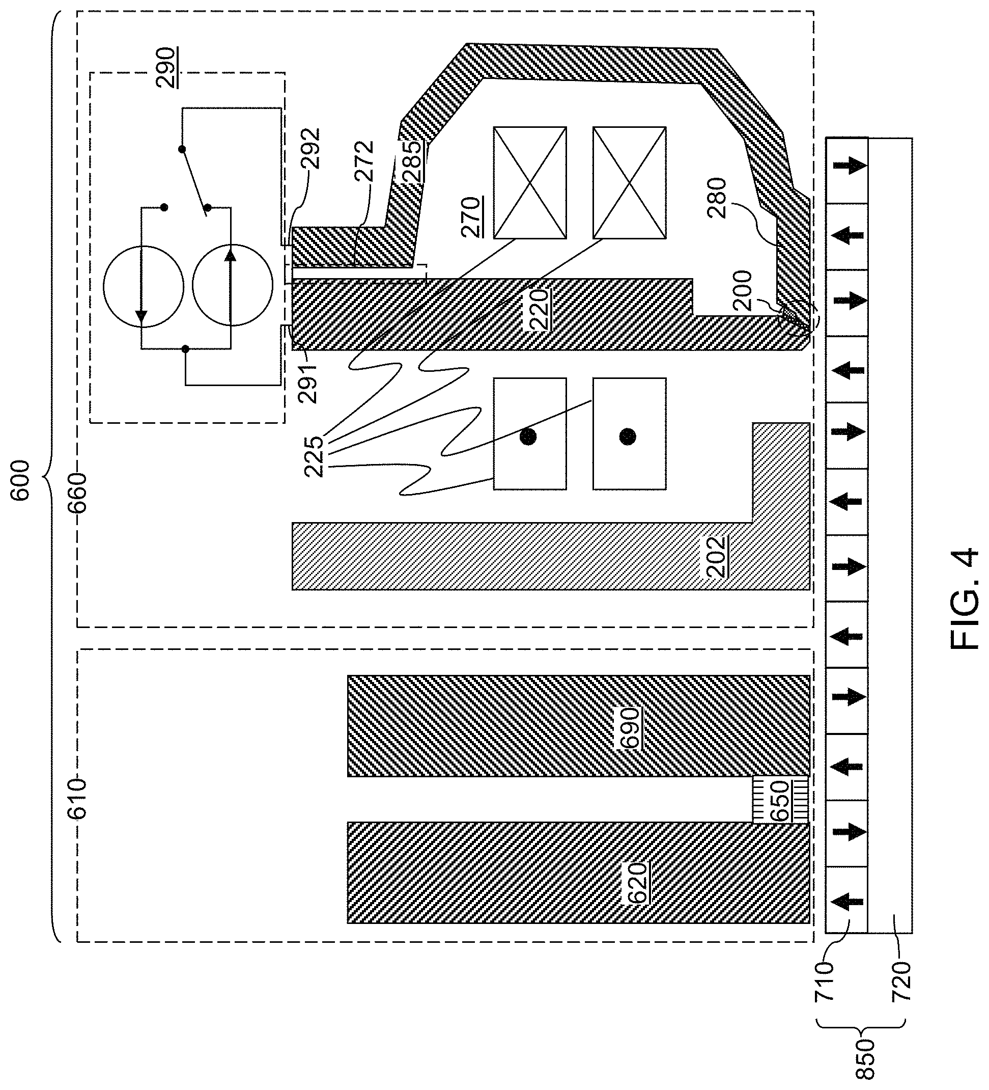
FIGS. 5A and 5B show magnified views of a first exemplary embodiment of the recording head 660 of a MAMR system that includes a record element 200 according to a first embodiment of the present disclosure. The main pole 220 is configured to emit a recording magnetic field for affecting the magnetic medium of the magnetic recording layer 710 (shown in FIG. 4). When electrical current passes through the magnetic coil 225, the magnetic field generated by the electrical current through the magnetic coil 225 magnetizes the soft magnetic material of the main pole 220, and the magnetic field is guided by through the main pole 220 and the trailing shield 280 to complete a magnetic loop.
As shown in FIG. 5B, the record element 200 includes a spin torque oscillator (STO) stack 250 located on a trailing sidewall of the main pole 220 in a gap between the main pole and the trailing shield. Side magnetic shields (also known as wrap around shield, WAS) 206 can be provided around the main pole 220 without physically contacting the main pole 220. A gap 205 which can be filled with a non-magnetic material, such as a dielectric material, for example aluminum oxide, is provided between the main pole 220 and each of the seed layer 207 and the side magnetic shields 206. The side magnetic shields 206 can be provided on the sides of the main pole 220, and may contact an electrically conductive seed layer 207 and the trailing shield 280. The trailing shield 280 is a magnetic shield located on a trailing sidewall of the spin torque oscillator 250 stack.
The main pole 220 is configured to serve as a first electrode of an electrical circuit, and the trailing shield 280 is configured to serve as a second electrode of the electrical circuit. The electrical circuit is biased by the bias circuitry 290, which is configured to provide electrical current between the main pole 220 and the trailing shield 280/upper pole 285 through the record element 200 in two opposite directions, which correspond to the two opposite magnetization directions that the record element 200 can induce in the magnetic medium to be recorded. An air bearing surface (ABS) of the magnetic head 600 includes planar surfaces of the main pole 220, the spin torque oscillator 250, and the magnetic shield as embodied as the trailing shield 280. Thus, the spin torque oscillator is exposed to the ABS. The planar surfaces can be within a same two-dimensional plane that provided by lapping during a manufacturing process.
As shown in the inset in FIG. 5A, according to an aspect of the present disclosure, a first electrically conductive path ECP1 is present through the spin torque oscillator 250 stack between the first electrode (as embodied as the main pole 220) and the second electrode (as embodied as the trailing shield 280). A second electrically conductive path ECP2 in a parallel connection with the first electrically conductive path ECP1 is present between the first electrode and the second electrode through a conductive material portion 360. Preferably but not necessarily, the conductive material portion 360 includes an electrically conductive, non-magnetic metal or a non-magnetic metallic alloy. In one embodiment, the conductive material portion 360 does not include a material that generates an alternating magnetic field upon application of an electrical current therethrough.
In one embodiment, the conductive material portion 360 is located in the gap between the main pole 220 and the trailing shield 280. In one embodiment, the conductive material portion 360 is not exposed to the ABS and is spaced from the ABS by a portion of the trailing shield 280 and or by the STO 250. In one embodiment, the conductive material portion 360 contacts a leading surface of the trailing shield 280. In one embodiment, the conductive material portion 360 includes a non-magnetic electrically conductive material, which can be a non-magnetic metal such as copper, tungsten, ruthenium, chromium and/or any other non-magnetic metal or a non-magnetic metallic alloy.
In one embodiment, a conductive layer stack 350 can also be provided in the gap between the main pole 220 and the trailing shield 280 within the second electrically conductive path ECP2. The conductive layer stack 350 can have a same set of component layers as the spin torque oscillator 250 stack, and can be spaced from the spin torque oscillator 250 stack by a dielectric spacer 310. The dielectric spacer 310 includes a dielectric material such as aluminum oxide, silicon oxide, and/or silicon nitride, and prevents the conductive layer stack 350 from functioning as another spin torque oscillator stack. In one embodiment, the conductive material portion 360 causes a predominant portion of the magnetic flux through the main pole 220 to flow through the spin torque oscillator 250 stack, and significantly reduces the magnetic flux through the conductive layer stack 350. For this reason, spin torque effect in the conductive layer stack 350 is much less than the spin torque effect in the spin torque oscillator 250 stack.
In one embodiment, the conductive layer stack 350 and the spin torque oscillator 250 stack can be located directly on the trailing sidewall of the main pole 220 in the trailing gap 222 between the main pole and the trailing shield 280. The conductive material portion 360 can be located on a trailing sidewall of the conductive layer stack 350. In one embodiment, an interface between the spin torque oscillator 250 stack and the magnetic shield (as embodied as the trailing shield 280) can be within a same plane as an interface between the conductive layer stack 350 and the conductive material portion 360.
Referring to the inset in FIG. 5A, the main pole 220 can have a trailing edge taper such that the trailing edge of the main pole and the trailing gap 222 between the main pole 220 and the trailing shield 280 can be tapered (i.e., slanted) in a non-perpendicular direction compared to the ABS. For example, the trailing edge of the main pole 220 and the trailing gap 222 can extend in a direction which is inclined with respect to the plane of the ABS by an angle of 10 to 80 degrees, such as 30 to 60 degrees. The trailing shield 280 can have a "bump" structure at a throat portion which results in the narrowing of the trailing gap 222 adjacent to the ABS where the STO 250 is located. The bump structure which defines a short effective trailing shield throat height (eTH) that may range from 20 nm to 150 nm. The shortest dimension in the direction into the air bearing surface (ABS) that determines the current path can be defined by either the eTH (if the bump material is non-conducting), or back edge position of the conducting trailing gap (if it is patterned and shorter than eTH), or both (if the two coincide).
Above the STO 250 and above the bump in the trailing shield 280, the trailing gap 222 is wider (i.e., has a larger width) than the width of the trailing gap 222 adjacent to the bump (i.e., the throat portion) of the trailing shield 280. The conductive layer stack 350 and the conductive material portion 360 are located in the wider portions of the trailing gap 222 above the throat portion of the trailing shield 280 while the STO 250 stack is located adjacent to the throat portion of the trailing shield in the narrower portion of the trailing gap 222. Thus, the conductive layer stack 350 and the conductive material portion 360 electrically short the main pole 220 and the trailing shield 280 across the trailing gap 222.
The electrical bias circuitry 290 is configured to flow electrical current between the first electrode (embodied as the main pole 220) and the second electrode (embodied as the trailing shield 280) through the first electrically conductive path ECP1 and the second electrically conductive path ECP2 in a forward direction and in a reverse direction depending on selection of a bias direction by the switching elements of the electrical bias circuitry 290.
The spin torque oscillator 250 stack is configured to generate a high-frequency magnetic field which is superimposed with the recording magnetic field to record data to the magnetic medium when current flows through the first and second electrically conductive paths (ECP1, ECP2). The spin torque oscillator 250 stack can include any material layer stack that is effective for the purpose of generating the high-frequency magnetic field for superposition with the recording magnetic field. The combination of the high-frequency magnetic field with the recording magnetic field lowers the coercivity of the magnetic medium on a disk during the recording process.
In an illustrative example shown in FIG. 5B, the spin torque oscillator 250 stack can include a stack, from the side of the leading edge to the side of the trailing edge, an electrically conductive, non-magnetic seed layer 252, a spin polarized layer 256 that generates precession of magnetization during operation, a non-magnetic electrically conductive spacer layer 256, and an optional magnetic field generating layer 258. In an illustrative example, the non-magnetic conductive seed layer 252 can include a non-magnetic conductive material such as Cr, Ru, W, and Cu, the spin polarized layer can include a magnetic nickel-iron alloy, the non-magnetic conductive spacer layer 256 can include a non-magnetic conductive material such as Cu, and the optional field generating layer 258, if present, can include another magnetic nickel-iron alloy. If the field generating layer 258 is present, then another optional non-magnetic, electrically conductive spacer layer (e.g., copper spacer layer) may be located between layer 258 and the trailing shield 280.
The thickness of the non-magnetic conductive seed layer 252 can be in a range from 3 nm to 12 nm, although lesser and greater thicknesses can also be employed. The thickness of the spin polarized layer 256 can be in a range from 3 nm to 12 nm, although lesser and greater thicknesses can also be employed. The frequency of the magnetic field generated by the spin polarized layer 256 can be in a range from 10 GHz to 40 GHz, although lesser and greater frequencies can be employed. The magnitude of the magnetic field generated by the spin polarized layer 256 can be in a range from 250 Gauss to 1,000 Gauss, although lesser and greater magnitudes can be employed for the magnetic field. The thickness of the non-magnetic conductive spacer layer 256 may be in a range from 3 nm to 15 nm, although lesser and greater thicknesses can also be employed. The thickness of the field generating layer 258, if present, may be in a range from 3 nm to 12 nm, although lesser and greater thicknesses can also be employed. Additional layers may be optionally employed to enhance performance of the spin torque oscillator 250 stack.
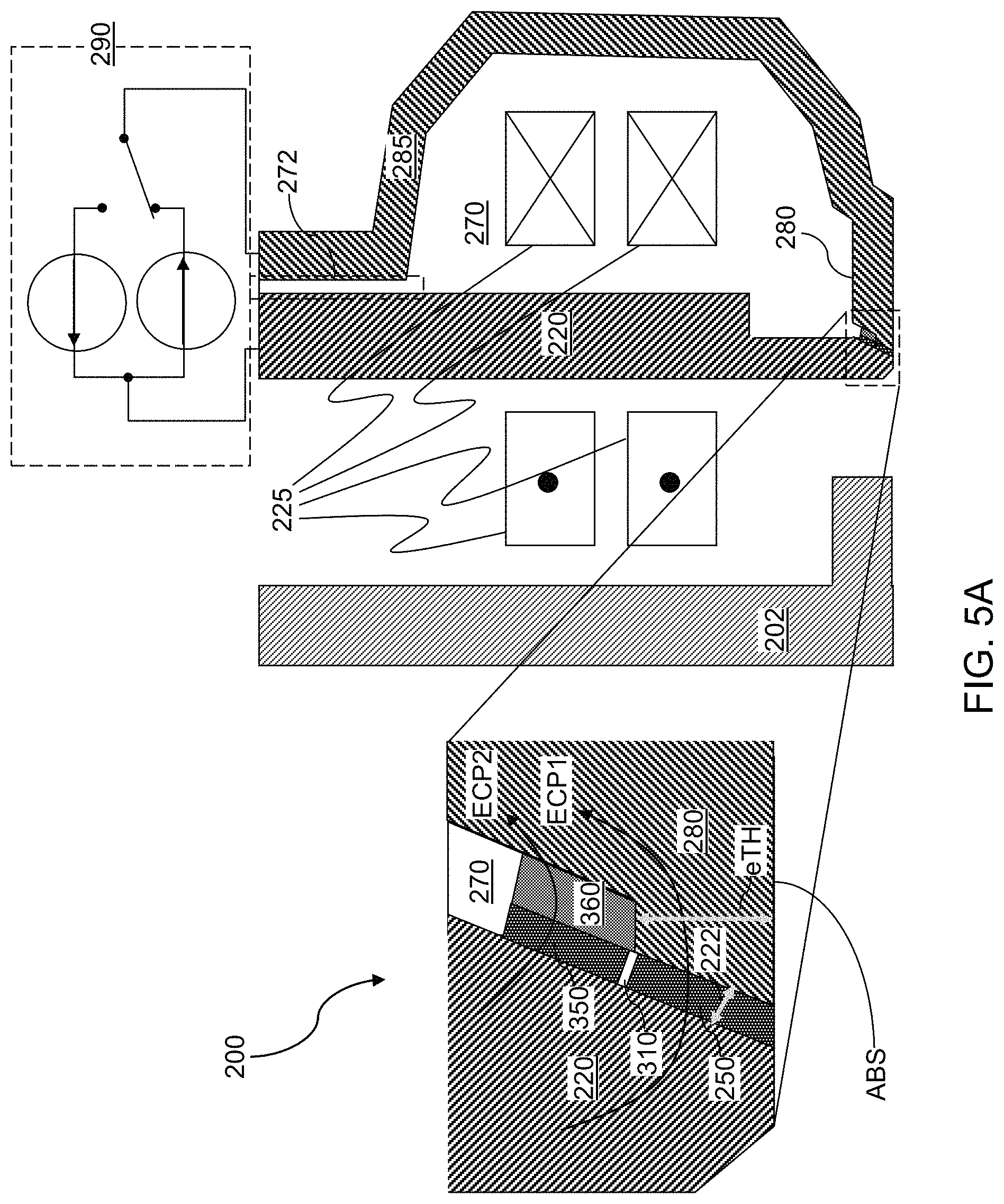
FIG. 6 shows magnified views of a second exemplary embodiment of a recording head 660 that includes a record element 200 according to a second embodiment of the present disclosure. The recording head 660 illustrated in FIG. 6 can be derived from the recording head 660 illustrated in FIGS. 5A and 5B by modifying the record element 200.
The recording head 660 of the second exemplary embodiment is the same as the recording head 660 of the first exemplary embodiment, except that the conductive layer stack 350 is replaced by a first conductive material portion 340, and the dielectric spacer 310 may be omitted. All other components of the recording head 660 of the second exemplary embodiment are the same as those of the recording head 660 of the first exemplary embodiment and will not be repeated herein for brevity.
The first conductive material portion 340 is provided within the second electrically conductive path ECP2. The first conductive material portion 340 is not exposed to the ABS and is spaced from the ABS by the spin torque oscillator 250 stack and/or the throat portion of the trailing shield 280. Preferably but not necessarily, the first conductive material portion 340 includes an electrically conductive non-magnetic metal (e.g., copper) or a non-magnetic metallic alloy. Alternatively, the first conductive material portion 340 can include a conductive multilayer stack of non-magnetic layers. In one embodiment, the first conductive material portion 340 does not include a material that generates an alternating magnetic field upon application of an electrical current therethrough.
In one embodiment, the first conductive material portion 340 contacts the trailing sidewall of the main pole 220 and a rear sidewall of the spin torque oscillator 250 stack that is located on an opposite side of the STO 250 stack from the ABS. The second conductive material portion 360 can be located on a trailing sidewall of the first conductive material portion 340 and contact the trailing shield 280. Thus, the first and the second conductive material portions 340, 360 electrically short the main pole 220 to the trailing shield 280. In one embodiment, an interface between the spin torque oscillator 250 stack and the trailing shield 280 can be within the same plane as an interface between the first conductive material portion 340 and the second conductive material portion 360. In one embodiment, the first conductive material portion 340 and the spin torque oscillator 250 stack can be located directly on the trailing sidewall of the main pole 220. The STO 250 stack is located in the trailing gap 222 adjacent to the throat portion of the trailing shield 280, while the first and the second conductive material portions 340, 360 are not exposed to the ABS and are located in the wider portion of the gap above the throat portion of the trailing shield 280.
The electrical bias circuitry 290 is configured to flow electrical current between the first electrode (embodied as the main pole 220) and the second electrode (embodied as the trailing shield 280/upper pole 285) through the first electrically conductive path ECP1 and the second electrically conductive path ECP2 in a forward direction and in a reverse direction depending on selection of a bias direction. The spin torque oscillator 250 stack can have the same configuration as, and provide the same function as, in the first embodiment.
In an alternative embodiment, first and the second conductive material portions 340, 360 may be replaced by single electrically conductive, non-magnetic layer, such as copper. Thus, a single electrically conductive, non-magnetic layer may be located in the trailing gap 222 in addition to the STO 250.
FIGS. 7A and 7B show magnified views of a third exemplary embodiment of a recording head 660 that includes a conductive material portion 360 as a read element according to a third embodiment of the present disclosure. The recording head 660 illustrated in FIGS. 7A and 7B can be derived from the recording head 660 illustrated in FIGS. 5A and 5B by modifying the record element 200.
The recording head 660 of the third exemplary embodiment is the same as the recording head 660 of the first exemplary embodiment, except that the STO 250 and the conductive layer stack 350 are replaced by a conductive material portion 360, and the dielectric spacer 310 may be omitted. All other components of the recording head 660 of the second exemplary embodiment are the same as those of the recording head 660 of the first exemplary embodiment and will not be repeated herein for brevity. Thus, since the STO 250 is omitted, the system of the third embodiment is not a MAMR system.
Preferably but not necessarily, the conductive material portion 360 includes at least one electrically conductive, non-magnetic material layer, such as at least one metal (e.g., copper, gold, platinum, ruthenium, chromium or tungsten) layer or a non-magnetic metallic alloy layer, such as a single electrically conductive non-magnetic material layer. Alternatively, the conductive material portion 360 can include a conductive multilayer stack of non-magnetic layers, or a multilayer stack of electrically conductive, magnetic and non-magnetic layers. In one embodiment, the conductive material portion 360 does not include a material that generates an alternating magnetic field upon application of an electrical current therethrough.
The record element 200 can consist of only the conductive layer 360, which is located on a trailing sidewall of the main pole 220. Side magnetic shields 206 can be provided around the main pole 220 tip without physically contacting the main pole 220 as illustrated in FIG. 7B. The side magnetic shields 206 can be provided on the sides of the main pole 220, and may contact the seed layer 207 and the trailing shield 280. A gap 205 filled with a dielectric is provided between the main pole 220 and each of the seed layer 207 and the side magnetic shields 206. The trailing shield 280 is a magnetic shield located on a trailing sidewall of the spin torque oscillator 250 stack.
The main pole 220 is configured to serve as a first electrode of an electrical circuit, and the trailing shield 280 is configured to serve as a second electrode of the electrical circuit. The electrical circuit is biased by the bias circuitry 290, which is configured to provide electrical current through the main pole 220 and the trailing shield 280/upper pole 285 in two opposite directions, which correspond to the two opposite magnetization directions that the record element 200 can induce in the magnetic medium to be recorded. An air bearing surface (ABS) of the magnetic head 600 includes planar surfaces of the main pole 220, the conductive material portion (e.g., the non-magnetic conductive layer) 360, and the trailing shield 280. Thus, in this embodiment, the conductive material portion 360 is exposed to the ABS. The planar surfaces can be within a same two-dimensional plane that provided by lapping during a manufacturing process. In one embodiment, the conductive layer 360 located in the trailing gap 222 contacts the trailing sidewall of the main pole 220 and a leading sidewall of trailing shield 280 to electrically short them.
According to an aspect of the present disclosure, an electrically conductive path ECP is present through the conductive layer 360 between the first electrode (as embodied as the main pole 220) and the second electrode (as embodied as the trailing shield 280). The electrical bias circuitry 290 is configured to flow electrical current between the first electrode (embodied as the main pole 220) and the second electrode (embodied as the trailing shield 280) through the electrically conductive path ECP in a forward direction and in a reverse direction depending on selection of a bias direction.
In one embodiment, a distal end of the main pole 220 and a distal end of the trailing magnetic shield 280, can be located on an opposite side of the air bearing surface ABS. The distal end of the main pole 220 which is connected to one electrical contact 291 can be an end portion of the first electrode the electrical bias circuitry 290, and the distal end of the trailing shield 280 which is connected to another electrical contact 292 of the electrical bias circuitry 290 can be an end portion of the second electrode. The electrically conductive path ECP through the conductive layer 360 (i.e., through the record element 200 which consists of only layer 360) can be the only path that provides electrical conduction between the distal end of the main pole 220 and the distal end of the trailing magnetic shield 280 for conduction of electrical current through the main pole. In one embodiment, an electrically insulating material layer 272 can provide physical isolation and electrical isolation between the distal end of the main pole 220 and the distal end of the upper pole 285.
The record element 200 of the first, second and/or third embodiments may be incorporated into the magnetic head 600 shown in FIG. 4. A magnetic storage device can be provided, which includes the magnetic head 600 incorporating the features of the first, second or third exemplary recording head 660, the magnetic medium which may be embodied as the magnetic recording layer 710 of the recording track 840 of a disk medium 850, a drive mechanism for passing the magnetic medium over the magnetic head 600, and a controller electrically coupled to the magnetic head 600 for controlling operation of the magnetic head 600 as illustrated in FIGS. 2 and 3.
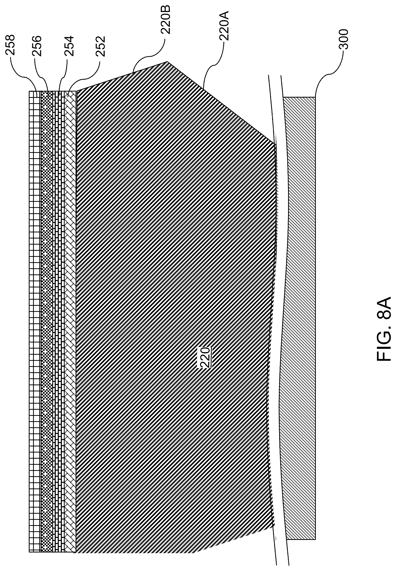
FIGS. 8A-8F illustrate a sequence of processing steps that can be employed to manufacture the first exemplary recording head. Referring to FIG. 8A, an auxiliary pole 202, side magnetic shields 206, and a dielectric material filling a portion of the gap 205 between the main pole 220 and the side magnetic shields 206 (not shown for clarity) are formed over a substrate 300. The main pole 220 is subsequently formed within a groove formed in the dielectric material. In one embodiment, the main pole 220 may have a leading edge tapered surface 220A (which may be supported by the side magnetic shield 206 and/or by a dielectric layer, which is not shown for clarity) and a trailing edge tapered surface 220B. Subsequently, a layer stack of component layers (252, 254, 256, 258) for forming a spin torque oscillator stack can be formed on a top (i.e., trailing) surface of the main pole 220, which is a trailing sidewall of the main pole 220. The layer stack may extend over the trailing edge tapered surface 220B of the main pole (not shown for clarity). Specifically, the non-magnetic conductive seed layer 252, the spin polarized layer 256 that generates precession of magnetization during operation, the non-magnetic conductive spacer layer 256, and the optional field generating layer 258 can be sequentially deposited. The composition and the thickness of the various component layers (252, 254, 256, 258) for the spin torque oscillator 250 stack can be as described above. The various component layers (252, 254, 256, 258) can be formed by conformal and/or non-conformal deposition process such as chemical vapor deposition (CVD), atomic layer deposition (ALD), physical vapor deposition (PVD), and/or various plating methods.
Referring to FIG. 8B, the layer stack of component layers (252, 254, 256, 258) for forming the spin torque oscillator stack can be patterned by a combination of a lithographic patterning process and an etch process. For example, a photoresist layer (not shown) can be applied over the spin torque oscillator 250 stack, and can be lithographically patterned to cover two discrete portions near an edge of the main pole 220 that is proximal to the air bearing surface to be subsequently formed. The gap between the two discrete portions of the patterned photoresist layer can have the dimension of the width of the dielectric spacer 310 to be subsequently formed, and may be in a range from 15 nm to 60 nm, although lesser and greater widths can also be employed. The pattern in the photoresist layer is transferred to through the layer stack of component layers (252, 254, 256, 258) by the etch process. For example, an ion milling process that employs the patterned photoresist layer as an etch mask can be employed to pattern the layer stack of component layers (252, 254, 256, 258).
A continuous remaining portion of the layer stack of component layers (252, 254, 256, 258) located at the air bearing surface side constitutes the spin torque oscillator 250 stack, which is a mesa structure. Another continuous remaining portion of the layer stack of component layers (252, 254, 256, 258) located adjacent to the spin torque oscillator 250 stack constitutes the conductive layer stack 350, which is another mesa structure. A trench 309 is provided between the spin torque oscillator 250 stack and the conductive layer stack 350. A field region 269 is provided, which includes a physically exposed top surface of the main pole 220 and is free of remaining portions of the layer stack of component layers (252, 254, 256, 258). The conductive layer stack 350 has a same set of component layers (252, 254, 256, 258) as the spin torque oscillator 250 stack.
Referring to FIG. 8C, a dielectric material can be deposited in the trench 309 and in the field region 269. Excess portions of the dielectric material can be removed from above the top surfaces of the conductive layer stack 350 and the spin torque oscillator 250 stack by a planarization process such as chemical mechanical planarization (CMP). The remaining portion of the dielectric material in the trench 309 constitutes the dielectric spacer 310. The remaining portion of the dielectric material in the field region 269 constitutes a first dielectric material portion 270A. The dielectric spacer 310 and the first dielectric material portion 270A include a dielectric material such as aluminum oxide, silicon oxide, or silicon nitride. The conductive layer stack 350 is spaced from the spin torque oscillator 250 stack by the dielectric spacer 310.
Referring to FIG. 8D, another dielectric material can be deposited and patterned to form a second dielectric material portion 270B, which can be formed directly on the top surface of the first dielectric material portion 270A. The second dielectric material portion 270B includes a dielectric material such as aluminum oxide, silicon oxide, or silicon nitride. The first and second dielectric material portions (270A, 270B) can be components of the insulating material portion 270. An electrically conductive, non-magnetic material can be deposited over the top surface of the conductive layer stack 350. For example, a lithographic patterning process can be performed to form a patterned photoresist layer including an opening within the area of the conductive layer stack 350. The conductive material can be deposited in the opening in the photoresist layer, and the photoresist layer can be lifted off to form the conductive material portion 360 described above. Alternatively, a non-conductive material layer may be deposited as a continuous layer, and can be patterned by a combination of a lithographic patterning process and an etch (e.g., ion milling) process to provide the conductive material portion 360. In this case, the second dielectric material portion 270B can be formed before or after forming the conductive material portion 360. In one embodiment, the conductive material portion 360 does not physically contact the spin torque oscillator 250 stack.
Preferably but not necessarily, the conductive material portion 360 includes a non-magnetic metal or a non-magnetic metallic alloy. Alternatively, the conductive material portion 360 can include a conductive multilayer stack of non-magnetic layers. In one embodiment, the conductive material portion 360 does not include a material that generates an alternating magnetic field upon application of an electrical current therethrough.
In one embodiment, the conductive material portion 360 can have a homogeneous composition throughout. In one embodiment, the conductive material portion 360 can comprise, and/or consist essentially of, copper, tungsten, ruthenium, chromium, and/or any other non-magnetic metal or a non-magnetic metallic alloy. The thickness of the conductive material portion 360 can be in a range from 20 nm to 200 nm, although lesser and greater thicknesses can also be employed. The conductive material portion 360 is formed over the trailing sidewall of the main pole 220, and directly on a trailing sidewall of the conductive layer stack 350.
Referring to FIG. 8E, the trailing shield 280 (which is a magnetic shield located on the side of the trailing sidewall of the spin torque oscillator 250 stack) can be formed. The trailing shield 280 can be formed directly on the top surfaces (which are trailing sidewalls) of the conductive material portion 360 and the spin torque oscillator 250 stack by deposition and patterning of a soft magnetic material. Subsequently, additional material layer can be deposited and patterned as needed. For example, components of the magnetic coil 225, additional portions of the insulating material portion 270 and the upper pole 285 can be formed and a recess in a trailing sidewall of the main pole can be formed by ion milling (not shown for clarity).
Referring to FIG. 8F, an air bearing surface (ABS) of the magnetic head 600 can be provided by lapping portions of the main pole 220, the spin torque oscillator 250 stack, and the trailing shield 280. As discussed above, the first electrically conductive path ECP1 includes the spin torque oscillator 250 stack, and the second electrically conductive path ECP2 includes the conductive layer stack 350 and the conductive material portion 360.
FIGS. 9A-9E illustrate a sequence of processing steps that can be employed to manufacture the second exemplary recording head. Referring to FIG. 9A, an exemplary structure that can be employed to form the second exemplary recording head is shown, which can be the same as the exemplary structure shown in FIG. 8A.
Referring to FIG. 9B, the layer stack of component layers (252, 254, 256, 258) for forming the spin torque oscillator stack can be patterned by a combination of a lithographic patterning process and an etch process. For example, a photoresist layer (not shown) can be applied over the spin torque oscillator 250 stack, and can be lithographically patterned to cover a discrete portion near an edge of the main pole 220 that is proximal to the air bearing surface to be subsequently formed. The pattern in the photoresist layer is transferred to through the layer stack of component layers (252, 254, 256, 258) by the etch process. For example, an ion milling process that employs the patterned photoresist layer as an etch mask can be employed to pattern the layer stack of component layers (252, 254, 256, 258). A continuous remaining portion of the layer stack of component layers (252, 254, 256, 258) located at the air bearing surface side constitutes the spin torque oscillator 250 stack, which is a mesa structure. A field region 269 is provided, which includes a physically exposed top surface of the main pole 220 and is free of remaining portions of the layer stack of component layers (252, 254, 256, 258).
Referring to FIG. 9C, a first electrically conductive, non-magnetic material can be deposited over a physically exposed top surface of the main pole 220 adjacent to the spin torque oscillator 250 stack. For example, a lithographic patterning process can be performed to form a patterned photoresist layer including an opening adjacent to the spin torque oscillator 250 stack. The first conductive material can be deposited in the opening in the photoresist layer, and the photoresist layer can be lifted off. The remaining portion of the first conductive material constitutes a first conductive material portion 340. Alternatively, the first conductive material layer may be deposited as a continuous layer, and can be patterned by a combination of a lithographic patterning process and an etch (e.g., ion milling) process to provide the first conductive material portion 340.
Preferably, but not necessarily, the first conductive material portion 340 includes a non-magnetic metal or a non-magnetic metallic alloy. Alternatively, the first conductive material portion 340 can include a conductive multilayer stack of non-magnetic layers. In one embodiment, the first conductive material portion 340 does not include a material that generates an alternating magnetic field upon application of an electrical current therethrough. In one embodiment, the first conductive material layer includes a non-magnetic conductive material such as copper, ruthenium, chromium, tungsten, another non-magnetic elemental metal, or a non-magnetic alloy thereof.
In one embodiment, the first conductive material portion 340 can contact a sidewall of the spin torque oscillator 250 stack. In one embodiment, the top surface of the first conductive material portion 340 may be planarized. In this case, the top surface of the first conductive material portion 340 can be coplanar with the top surface of the spin torque oscillator 250 stack. In one embodiment, the first conductive material portion 340 can comprise, and/or consist essentially of, copper, tungsten, ruthenium, chromium, and/or any other non-magnetic metal or a non-magnetic metallic alloy. The first conductive material portion 340 is formed directly on a trailing sidewall of the main pole 220.
Referring to FIG. 9D, a dielectric material can be deposited in the region that is not covered by the spin torque oscillator 250 stack or the first conductive material portion 340. The dielectric material can be deposited as a continuous material layer, and excess portions of the dielectric material can be removed from above the first conductive material portion 340 and the spin torque oscillator 250 stack by a masked etch process. The remaining portion of the dielectric material constitutes a dielectric material portion 270C, which can be a portion of the insulating material portion 270.
A second electrically conductive, non-magnetic material can be deposited on the first conductive material portion 340. For example, a lithographic patterning process can be performed to form a patterned photoresist layer including an opening overlying the first conductive material portion 340. The second conductive material can be deposited in the opening in the photoresist layer, and the photoresist layer can be lifted off. The remaining portion of the second conductive material constitutes a second conductive material portion 360. Alternatively, the second conductive material layer may be deposited as a continuous layer, and can be patterned by a combination of a lithographic patterning process and an etch (e.g., ion milling) process to provide the second conductive material portion 360.
Preferably but not necessarily, the second conductive material portion 360 includes a non-magnetic metal or a non-magnetic metallic alloy. Alternatively, the second conductive material portion 360 can include a conductive multilayer stack of non-magnetic layers, or a conductive multilayer stack of magnetic layers. In one embodiment, the second conductive material portion 360 does not include a material that generates an alternating magnetic field upon application of an electrical current therethrough. In one embodiment, the second conductive material portion 360 includes a non-magnetic conductive material such as copper, ruthenium, chromium, tungsten, another non-magnetic elemental metal, or a non-magnetic alloy thereof. The second conductive material portion 360 can include the same material as, or a different material from, the first conductive material portion 340. In one embodiment, the second conductive material portion 360 can have a homogeneous composition throughout. In one embodiment, the second conductive material portion 360 can comprise, and/or consist essentially of, copper, tungsten, ruthenium, chromium, and/or any other non-magnetic metal or a non-magnetic metallic alloy. The thickness of the second conductive material portion 360 can be in a range from 20 nm to 200 nm, although lesser and greater thicknesses can also be employed. The second conductive material portion 360 is formed over the main pole 220, and directly on a trailing sidewall of the first non-magnetic conductive material portion 340.
Referring to FIG. 9E, the trailing shield 280 (which is a magnetic shield located on the side of the trailing sidewall of the spin torque oscillator 250 stack) can be formed. The trailing shield 280 can be formed directly on the top surfaces (which are trailing sidewalls) of the conductive material portion 360 and the spin torque oscillator 250 stack by deposition and patterning of a soft magnetic material. Subsequently, additional material layers can be deposited and patterned as needed. For example, components of the magnetic coil 225, additional portions of the insulating material portion 270 and the upper pole 285 can be formed and a recess in a trailing sidewall of the main pole can be formed by ion milling (not shown for clarity).
An air bearing surface (ABS) of the magnetic head 600 can be provided by lapping portions of the main pole 220, the spin torque oscillator 250 stack, and the trailing shield 280. As discussed above, the first electrically conductive path ECP1 includes the spin torque oscillator 250 stack, and the second electrically conductive path ECP2 includes the first and second conductive material portions (340, 360).
FIGS. 10A-10C illustrate a sequence of processing steps that can be employed to manufacture the third exemplary recording head. Referring to FIG. 10A, an auxiliary pole 202, side magnetic shields 206, and a dielectric material filling a portion of the gap 205 between the main pole 220 and the auxiliary pole 202 and the side magnetic shields 206 are formed over a substrate (not shown). The main pole 220 is subsequently formed within a groove formed in the dielectric material.
Subsequently, an electrically conductive, non-magnetic material can be deposited on the air bearing side of the top surface of the main pole 220. For example, the conductive material layer may be deposited as a continuous layer, and can be patterned by a combination of a lithographic patterning process and an etch (e.g., ion milling) process to provide a conductive material portion 360. Alternatively, the conductive material portion 360 can be formed by a lift-off process. Preferably but not necessarily, the conductive material portion 360 includes a non-magnetic metal or a non-magnetic metallic alloy. Alternatively, the conductive material portion 360 can include a conductive multilayer stack of non-magnetic layers, or a conductive multilayer stack of magnetic layers. In one embodiment, the conductive material portion 360 does not include a material that generates an alternating magnetic field upon application of an electrical current therethrough. In one embodiment, the conductive material portion 360 includes a non-magnetic conductive material such as copper, gold, platinum, ruthenium, chromium, tungsten, another non-magnetic elemental metal, or a non-magnetic alloy thereof. In one embodiment, the conductive material portion 360 can comprise, and/or consist essentially of, copper, gold, platinum, tungsten, ruthenium, chromium, and/or any other non-magnetic metal or a non-magnetic metallic alloy. The conductive material portion 360 is formed directly on a trailing sidewall of the main pole 220.
Referring to FIG. 10B, a dielectric material can be deposited in the region that does not overlap with the conductive material portion 360. The dielectric material can be deposited as a continuous material layer, and excess portions of the dielectric material can be removed from above the conductive material portion 360 by a masked etch process. Alternatively, a patterned mask layer including an opening adjacent to the conductive material portion 360 can be formed. A dielectric material can be deposited within the opening, and the patterned mask layer can be lifted off. The remaining portion of the dielectric material constitutes a dielectric material portion 270D, which can be a portion of the insulating material portion 270. The dielectric material portion 270D includes a dielectric material such as aluminum oxide, silicon oxide, or silicon nitride.
Referring to FIG. 10C, the trailing shield 280 (which is a magnetic shield located on the side of the trailing sidewall of the spin torque oscillator 250 stack) can be formed. The trailing shield 280 can be formed directly on the top surface (which is the trailing sidewall) of the conductive material portion 360 by deposition and patterning of a soft magnetic material. Subsequently, additional material layers can be deposited and patterned as needed. For example, components of the magnetic coil 225, additional portions of the insulating material portion 270 and the upper pole 285 can be formed and a recess in a trailing sidewall of the main pole can be formed by ion milling (not shown for clarity).
An air bearing surface (ABS) of the magnetic head 600 can be provided by lapping portions of the main pole 220, the conductive material portion 360, and the magnetic shield (i.e., the trailing shield 280). As discussed above, the electrically conductive path ECP includes the magnetic conductive material portion 360.
The various recording heads of the present disclosure provide advantages over prior art recording heads by utilizing Ampere's field generated by electrical current through a conductive material portion 360. Specifically, the electrical current flowing between the main pole 220 and the trailing shield 280 generates the Ampere's field, which is employed to achieve significant areal density capability (ADC) gain. The areal density capability from the Ampere's field can be as large as, or can be greater than that of, microwave assisted magnetic recording (MAMR). The effect from the Ampere's field may be employed in combination with MAMR effects as in the first and second exemplary recording heads, or may be employed in lieu of MAMR effects as in the third exemplary recording head.
FIG. 11 shows magnetization M, bias current I, and the current induced Ampere's field in the main pole 220 and in the trailing shield 280 in the vicinity of a trailing gap 222, which includes the record element 200 containing the conductive material portion 360, for the third exemplary recording head. The principle of operation illustrated in FIG. 11 applies equally to the second electrically conductive path ECP2 of the first and second exemplary recording heads.
Referring back to FIGS. 5A, 5B, 6, 7A, and 7B, the main pole 220 and the trailing magnetic shield 280 can be in direct electric contact through the conducting trailing gap 222 containing the record element 200, which can consist of the conductive material portion 360 as in the third embodiment, or can include the conductive material portion 360 and the spin torque oscillator 250 stack and additional components as in the first and second embodiments. The main pole 220 and the trailing shield 280 are otherwise electrically insulated and isolated from each other. The main pole 220 constitutes a first electrode and the trailing shield 280/upper pole 285 constitutes a second electrode. When an electrical bias voltage is applied across the first and second electrodes, electrical current flows from the main pole 220 into the trailing shield 280, or vice versa through the record element 200.
In one embodiment, the insulating material layer 272 can be a thin dielectric layer such as an aluminum oxide layer, which is provided in the back gap area between end portions of the first electrode and the second electrode. The insulating material layer 272 can have a thickness in a range from 10 nm to 100 nm, such as from 20 nm to 50 nm, although lesser and greater thicknesses can also be employed. Additional insulating material can be provided in order to provide electrical isolation between the first electrode (as embodied as the main pole 220) and the second electrode (as embodied as the trailing shield 280).
During operation of the recording heads of the present disclosure, an electrical bias voltage is applied across the main pole 220 and the trailing shield 280. The electrical bias voltage induces electrical current between the main pole 220 and the trailing shield 280. This electrical current improves performance of the recording head with a higher ADC, as elaborated below. The electrical bias voltage across the main pole 220 and the trailing shield 280 can be a direct current (DC) bias voltage (with either polarity), or can be an alternating current (AC) bias voltage. In the case of an AC bias voltage, it is preferred to have a waveform that follows the waveform of the write current through the magnetic coil 225 per the bits to be written, either in-phase, or out of phase. In other words, an AC bias voltage can be applied as a pulse only during the transition in the magnetization during the recording process.
During operation of the recording heads of the present disclosure, an electric current flows from the main pole 220 into the trailing shield 280, or vice versa. As illustrated in FIG. 12, this current produces an Ampere field inside both the main pole 220 and the trailing shield 280, as well as in the recording media. FIG. 12 shows finite element model (FEM) simulation results of the bias current distribution and the Ampere's field (MP) produced by 5 mA of the bias current through the main pole according to an embodiment of the present disclosure. For a bias current of 5 mA (which corresponds to a bias voltage of 150 mV and a total resistance of 30 Ohm), a circular field inside the main pole 220 is clearly visible, with magnitude of .about.100 Oe at the ABS side, and .about.200 Oe in the back, which is consistent with the current density distribution (higher in the back and lower at the ABS).
Because of the small dimension defined by the bump position, the high current density is mainly concentrated inside the main pole 220 and the trailing shield 280 in the vicinity of the trailing gap 222 area, which is in the range of approximately from 100 nm to 150 nm into the air bearing surface (ABS). According to Ampere's law, this current will produce a circular magnetic field that is in the direction transverse to that of the current. Since the current direction is substantially the same as the direction of the magnetization of the main pole 220 and the trailing shield 280, this Ampere field is also transverse to the magnetization, thus producing a transverse magnetization component with respect to the flux flow direction in the main pole 220 and the trailing shield 280 around the trailing gap 222. This will in turn make faster the flux reversal in the main pole 220 and trailing shield 280.
In addition to the current induced Ampere field inside the recording head that makes the magnetization switching faster, the Ampere field also has other non-limiting benefits. One benefit is that the Ampere field could change the magnetization direction of the main pole and the trailing shield in the vicinity of the trailing gap, such that the flux shunt from the main pole 220 into the trailing shield 280 is reduced, leading to higher field (thus higher overwrite) in the media. Another benefit is that the media will also experience this Ampere's field.
Although the foregoing refers to particular preferred embodiments, it will be understood that the disclosure is not so limited. It will occur to those of ordinary skill in the art that various modifications may be made to the disclosed embodiments and that such modifications are intended to be within the scope of the disclosure. Where an embodiment employing a particular structure and/or configuration is illustrated in the present disclosure, it is understood that the present disclosure may be practiced with any other compatible structures and/or configurations that are functionally equivalent provided that such substitutions are not explicitly forbidden or otherwise known to be impossible to one of ordinary skill in the art. All of the publications, patent applications and patents cited herein are incorporated herein by reference in their entirety.
* * * * *
References
D00000
D00001
D00002
D00003
D00004
D00005
D00006
D00007
D00008
D00009
D00010
D00011
D00012

D00013

D00014

D00015
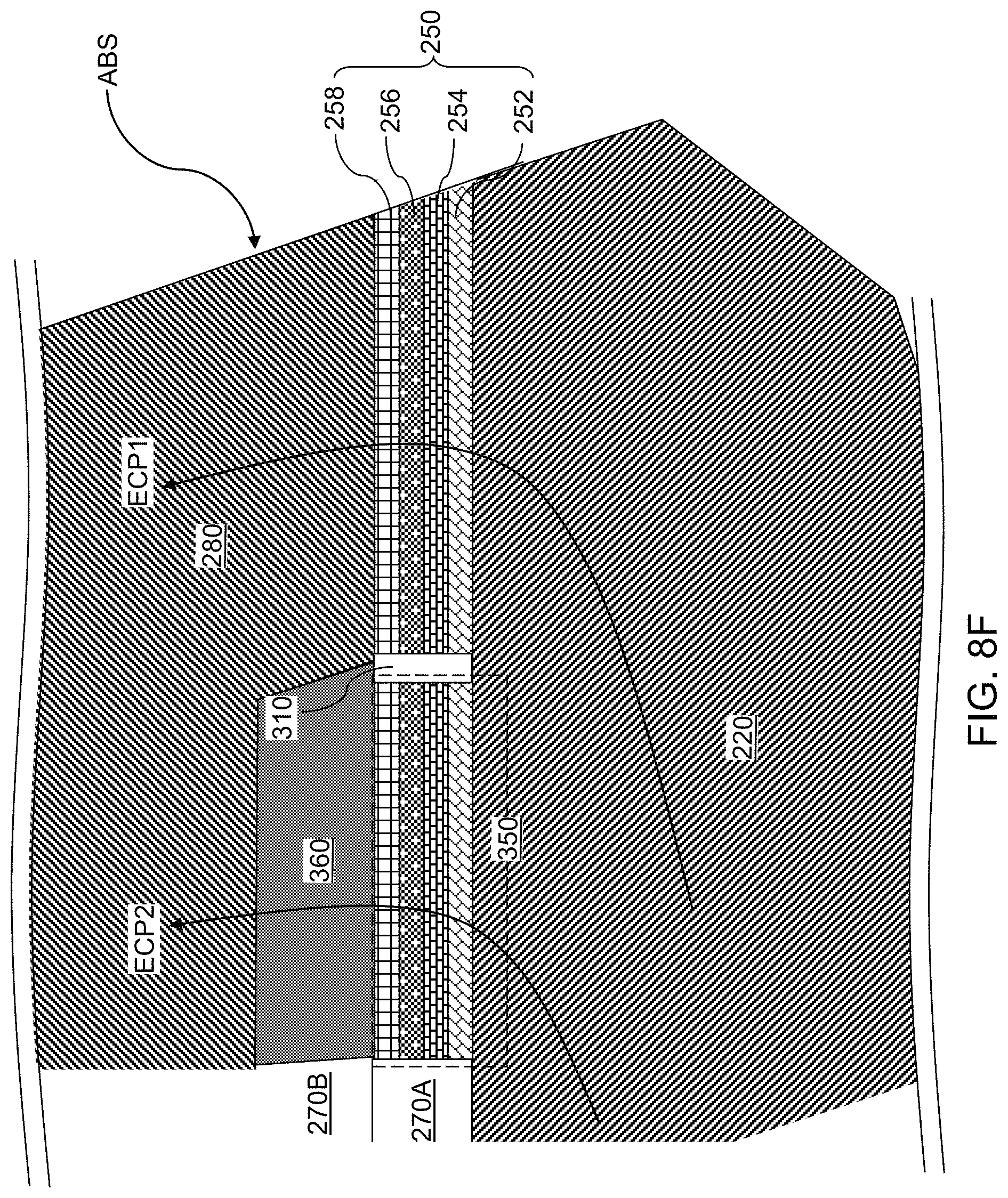
D00016
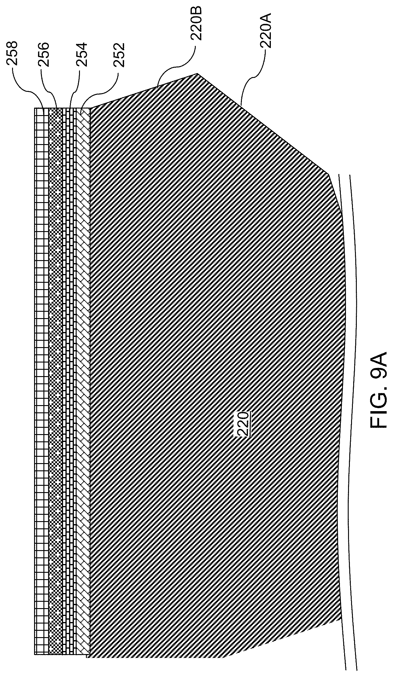
D00017

D00018
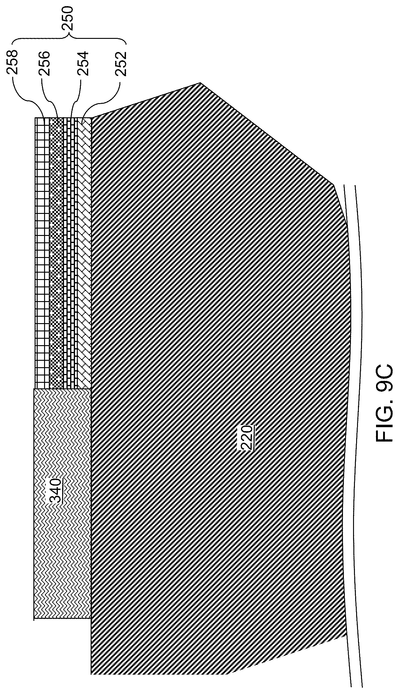
D00019

D00020
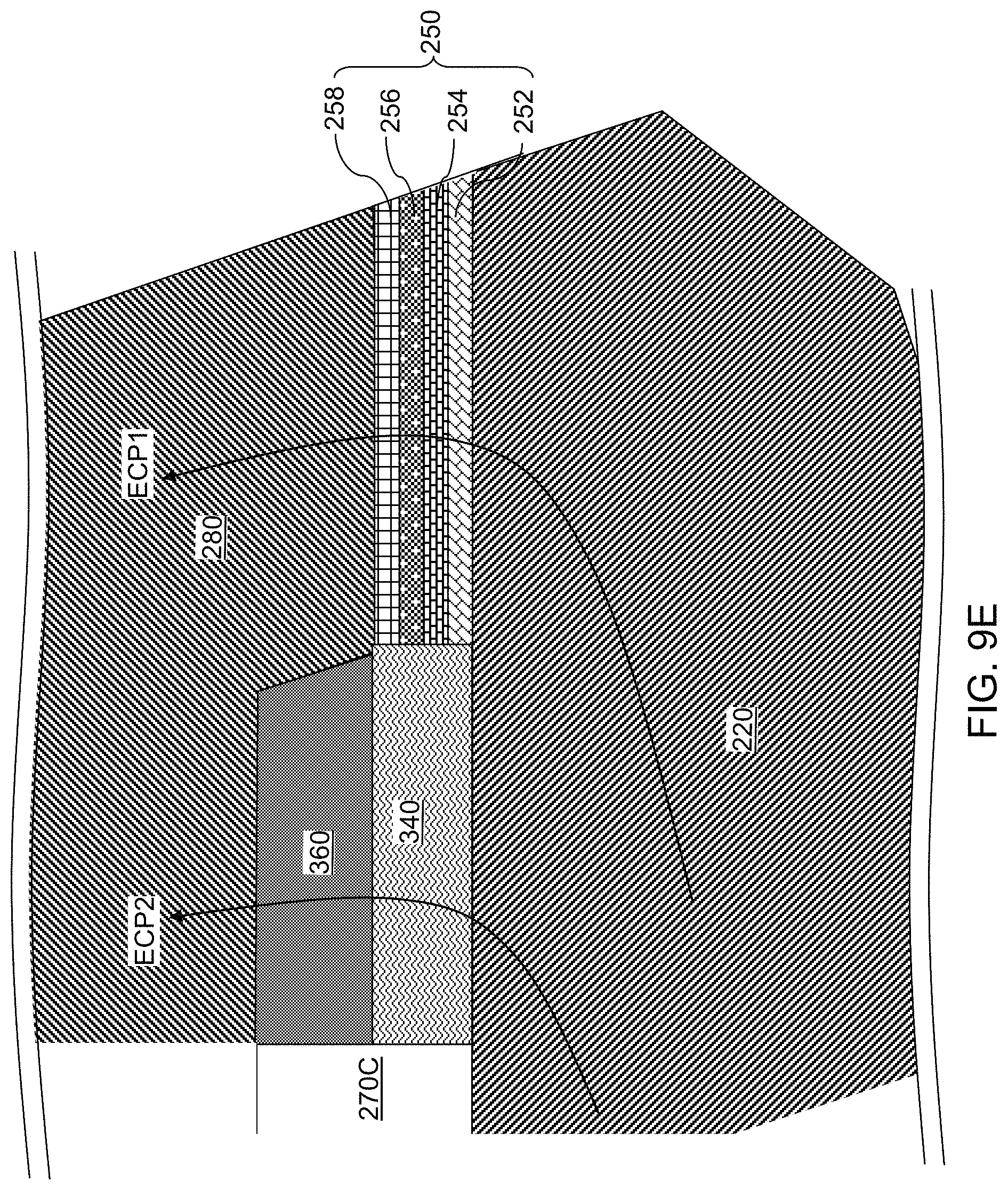
D00021
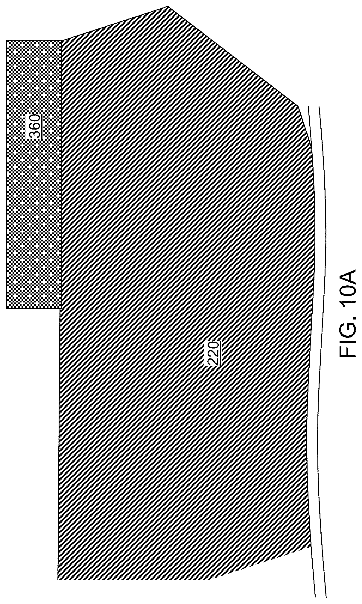
D00022
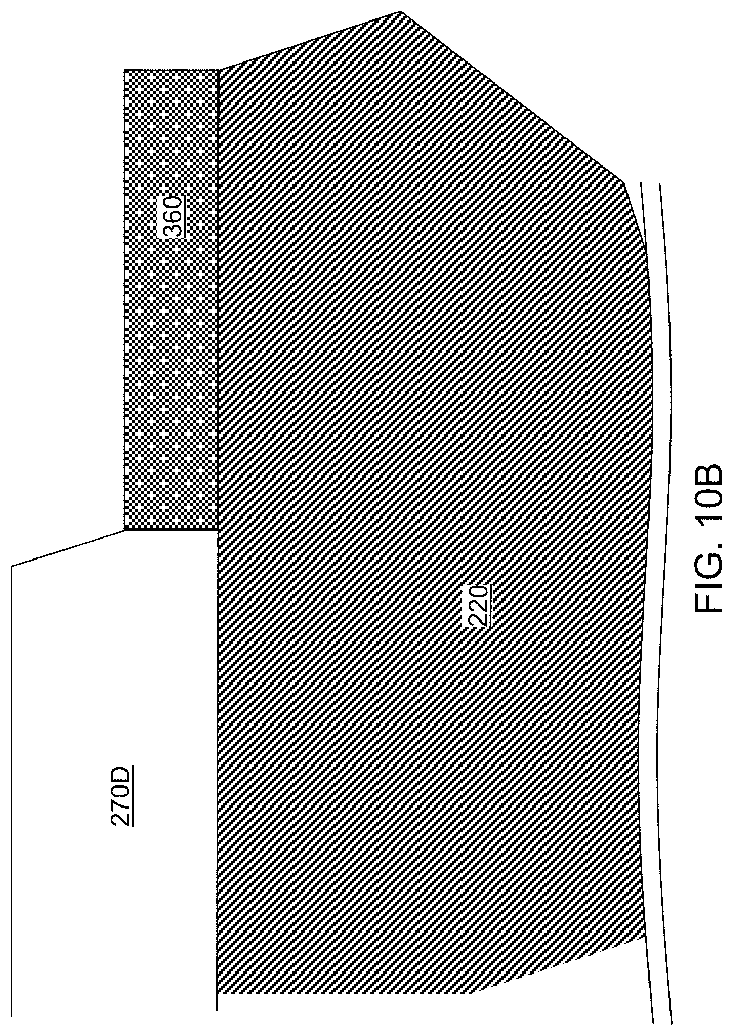
D00023
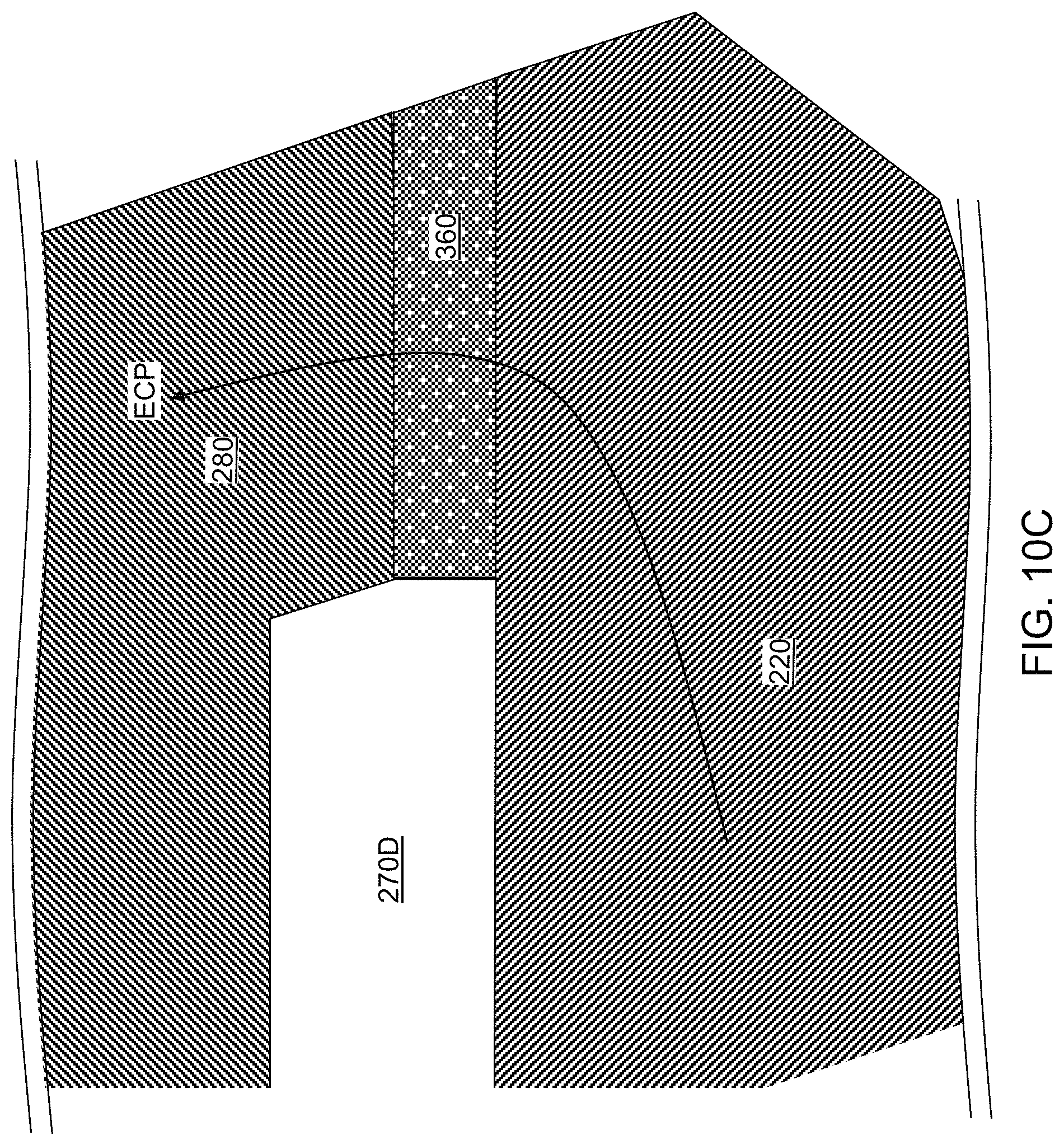
D00024

D00025

XML
uspto.report is an independent third-party trademark research tool that is not affiliated, endorsed, or sponsored by the United States Patent and Trademark Office (USPTO) or any other governmental organization. The information provided by uspto.report is based on publicly available data at the time of writing and is intended for informational purposes only.
While we strive to provide accurate and up-to-date information, we do not guarantee the accuracy, completeness, reliability, or suitability of the information displayed on this site. The use of this site is at your own risk. Any reliance you place on such information is therefore strictly at your own risk.
All official trademark data, including owner information, should be verified by visiting the official USPTO website at www.uspto.gov. This site is not intended to replace professional legal advice and should not be used as a substitute for consulting with a legal professional who is knowledgeable about trademark law.