Digital microfluidic devices including dual substrates with thin-film transistors and capacitive sensing
French January 5, 2
U.S. patent number 10,882,042 [Application Number 16/161,548] was granted by the patent office on 2021-01-05 for digital microfluidic devices including dual substrates with thin-film transistors and capacitive sensing. This patent grant is currently assigned to E Ink Corporation. The grantee listed for this patent is E Ink Corporation. Invention is credited to Ian French.


| United States Patent | 10,882,042 |
| French | January 5, 2021 |
Digital microfluidic devices including dual substrates with thin-film transistors and capacitive sensing
Abstract
An active matrix electrowetting on dielectric (AM-EWoD) device including dual substrates with thin-film transistors (TFT) and capacitive sensing. As depicted herein the bottom substrate includes a first plurality of electrodes to propel various droplets through a microfluidic region, while the top substrate includes a second plurality of electrodes that are configured to interrogate the droplets with capacitive sensing. In some embodiments, the top substrate has zones of high-resolution sensing and zones of low-resolution sensing.
| Inventors: | French; Ian (Hsinchu, TW) | ||||||||||
|---|---|---|---|---|---|---|---|---|---|---|---|
| Applicant: |
|
||||||||||
| Assignee: | E Ink Corporation (Billerica,
MA) |
||||||||||
| Family ID: | 66097311 | ||||||||||
| Appl. No.: | 16/161,548 | ||||||||||
| Filed: | October 16, 2018 |
Prior Publication Data
| Document Identifier | Publication Date | |
|---|---|---|
| US 20190111433 A1 | Apr 18, 2019 | |
Related U.S. Patent Documents
| Application Number | Filing Date | Patent Number | Issue Date | ||
|---|---|---|---|---|---|
| 62573846 | Oct 18, 2017 | ||||
| Current U.S. Class: | 1/1 |
| Current CPC Class: | H01L 27/1251 (20130101); G01R 27/2605 (20130101); B01L 3/502707 (20130101); B01L 3/50273 (20130101); B01L 3/502784 (20130101); B01L 3/5027 (20130101); G02B 26/005 (20130101); H01L 27/1248 (20130101); H01L 27/1255 (20130101); G02B 21/0076 (20130101); B01L 3/502792 (20130101); G09G 3/348 (20130101); B01L 2200/0673 (20130101); B01L 2400/0427 (20130101); B01L 2300/161 (20130101) |
| Current International Class: | B01L 3/00 (20060101); G02B 26/00 (20060101); G01R 27/26 (20060101); H01L 27/12 (20060101); G09G 3/34 (20060101) |
References Cited [Referenced By]
U.S. Patent Documents
| 4573995 | March 1986 | Chen et al. |
| 4708716 | November 1987 | Sibalis |
| 5080646 | January 1992 | Theeuwes et al. |
| 5311337 | May 1994 | McCartney, Jr. |
| 5930026 | July 1999 | Jacobson |
| 6118426 | September 2000 | Albert |
| 6124851 | September 2000 | Jacobson |
| 6130773 | October 2000 | Jacobson |
| 6177921 | January 2001 | Comiskey |
| 6232950 | May 2001 | Albert |
| 6241921 | June 2001 | Jacobson |
| 6252564 | June 2001 | Albert |
| 6312304 | November 2001 | Duthaler |
| 6312971 | November 2001 | Amundson |
| 6376828 | April 2002 | Comiskey |
| 6392786 | May 2002 | Albert |
| 6413790 | July 2002 | Duthaler |
| 6422687 | July 2002 | Jacobson |
| 6445374 | September 2002 | Albert |
| 6445489 | September 2002 | Jacobson |
| 6473072 | October 2002 | Comiskey |
| 6480182 | November 2002 | Turner |
| 6498114 | December 2002 | Amundson |
| 6504524 | January 2003 | Gates |
| 6506438 | January 2003 | Duthaler |
| 6512354 | January 2003 | Jacobson |
| 6518949 | February 2003 | Drzaic |
| 6521489 | February 2003 | Duthaler et al. |
| 6531997 | March 2003 | Gates |
| 6535197 | March 2003 | Comiskey |
| 6545291 | April 2003 | Amundson |
| 6639578 | October 2003 | Comiskey |
| 6657772 | December 2003 | Loxley |
| 6664944 | December 2003 | Albert |
| D485294 | January 2004 | Albert |
| 6680725 | January 2004 | Jacobson |
| 6683333 | January 2004 | Kazlas |
| 6704133 | March 2004 | Gates |
| 6710540 | March 2004 | Albert |
| 6724519 | April 2004 | Comiskey |
| 6738050 | May 2004 | Comiskey |
| 6750473 | June 2004 | Amundson |
| 6753999 | June 2004 | Zehner |
| 6816147 | November 2004 | Albert |
| 6819471 | November 2004 | Amundson |
| 6825068 | November 2004 | Denis |
| 6825829 | November 2004 | Albert |
| 6825970 | November 2004 | Goenaga |
| 6831769 | December 2004 | Holman |
| 6842167 | January 2005 | Albert |
| 6842279 | January 2005 | Amundson |
| 6842657 | January 2005 | Drzaic |
| 6865010 | March 2005 | Duthaler et al. |
| 6873452 | March 2005 | Tseng |
| 6900851 | May 2005 | Morrison |
| 6909532 | June 2005 | Chung |
| 6922276 | July 2005 | Zhang |
| 6950220 | September 2005 | Abramson et al. |
| 6967640 | November 2005 | Albert et al. |
| 6980196 | December 2005 | Turner et al. |
| 6982178 | January 2006 | LeCain et al. |
| 6995550 | February 2006 | Jacobson |
| 7002728 | February 2006 | Pullen |
| 7012600 | March 2006 | Zehner |
| 7012735 | March 2006 | Honeyman |
| 7023420 | April 2006 | Comiskey |
| 7030412 | April 2006 | Drzaic et al. |
| 7030854 | April 2006 | Baucom et al. |
| 7034783 | April 2006 | Gates |
| 7061166 | June 2006 | Kuniyasu |
| 7061662 | June 2006 | Chung |
| 7075502 | July 2006 | Drzaic |
| 7075703 | July 2006 | O'Neil et al. |
| 7106296 | September 2006 | Jacobson |
| 7110163 | September 2006 | Webber et al. |
| 7116318 | October 2006 | Amundson |
| 7116466 | October 2006 | Whitesides |
| 7119759 | October 2006 | Zehner et al. |
| 7119772 | October 2006 | Amundson |
| 7148128 | December 2006 | Jacobson |
| 7163612 | January 2007 | Sterling et al. |
| 7167155 | January 2007 | Albert |
| 7170670 | January 2007 | Webber |
| 7173752 | February 2007 | Doshi et al. |
| 7176880 | February 2007 | Amundson et al. |
| 7177066 | February 2007 | Chung |
| 7190008 | March 2007 | Amundson et al. |
| 7193625 | March 2007 | Danner |
| 7202847 | April 2007 | Gates |
| 7206119 | April 2007 | Honeyman et al. |
| 7223672 | May 2007 | Kazlas et al. |
| 7230751 | June 2007 | Whitesides |
| 7242514 | July 2007 | Chung |
| 7256766 | August 2007 | Albert et al. |
| 7259744 | August 2007 | Arango |
| 7280094 | October 2007 | Albert |
| 7301693 | November 2007 | Chaug |
| 7304780 | December 2007 | Liu |
| 7304787 | December 2007 | Whitesides |
| 7312784 | December 2007 | Baucom |
| 7312794 | December 2007 | Zehner |
| 7327346 | February 2008 | Chung |
| 7327511 | February 2008 | Whitesides |
| 7347957 | March 2008 | Wu |
| 7349148 | March 2008 | Doshi et al. |
| 7352353 | April 2008 | Albert |
| 7365394 | April 2008 | Denis et al. |
| 7365733 | April 2008 | Duthaler |
| 7382363 | June 2008 | Albert et al. |
| 7388572 | June 2008 | Duthaler et al. |
| 7401758 | July 2008 | Liang |
| 7408699 | August 2008 | Wang |
| 7411719 | August 2008 | Paolini, Jr. |
| 7420549 | September 2008 | Jacobson |
| 7442587 | October 2008 | Amundson et al. |
| 7453445 | November 2008 | Amundson |
| 7471274 | December 2008 | Kim |
| 7492339 | February 2009 | Amundson |
| 7492497 | February 2009 | Paolini, Jr. |
| 7528822 | May 2009 | Amundson |
| 7535624 | May 2009 | Amundson et al. |
| 7545358 | June 2009 | Gates |
| 7551346 | June 2009 | Fazel |
| 7554712 | June 2009 | Patry et al. |
| 7560004 | July 2009 | Pereira |
| 7583251 | September 2009 | Arango |
| 7583427 | September 2009 | Danner |
| 7598173 | October 2009 | Ritenour |
| 7602374 | October 2009 | Zehner |
| 7605799 | October 2009 | Amundson et al. |
| 7612760 | November 2009 | Kawai |
| 7636191 | December 2009 | Duthaler |
| 7649674 | January 2010 | Danner |
| 7667886 | February 2010 | Danner |
| 7672040 | March 2010 | Sohn |
| 7679599 | March 2010 | Kawai |
| 7679813 | March 2010 | Liang |
| 7679814 | March 2010 | Paolini, Jr. |
| 7683606 | March 2010 | Kang |
| 7688297 | March 2010 | Zehner |
| 7688497 | March 2010 | Danner |
| 7705824 | April 2010 | Baucom et al. |
| 7729039 | June 2010 | LeCain et al. |
| 7733311 | June 2010 | Amundson |
| 7733335 | June 2010 | Zehner |
| 7785988 | August 2010 | Amundson |
| 7787169 | August 2010 | Abramson et al. |
| 7830592 | November 2010 | Sprague |
| 7839564 | November 2010 | Whitesides et al. |
| 7843626 | November 2010 | Amundson et al. |
| 7859637 | December 2010 | Amundson et al. |
| 7859742 | December 2010 | Chiu |
| 7880958 | February 2011 | Zang |
| 7893435 | February 2011 | Kazlas et al. |
| 7898717 | March 2011 | Patry |
| 7905977 | March 2011 | Qi |
| 7952557 | May 2011 | Amundson |
| 7956841 | June 2011 | Albert |
| 7957053 | June 2011 | Honeyman |
| 7982479 | July 2011 | Wang |
| 7986450 | July 2011 | Cao |
| 7999787 | August 2011 | Amundson |
| 8009344 | August 2011 | Danner |
| 8009348 | August 2011 | Zehner |
| 8027081 | September 2011 | Danner |
| 8049947 | November 2011 | Danner |
| 8064962 | November 2011 | Wilcox et al. |
| 8072675 | December 2011 | Lin |
| 8077141 | December 2011 | Duthaler |
| 8089453 | January 2012 | Comiskey |
| 8120836 | February 2012 | Lin |
| 8125501 | February 2012 | Amundson |
| 8139050 | March 2012 | Jacobson |
| 8149228 | April 2012 | Lin et al. |
| 8159636 | April 2012 | Sun |
| 8159644 | April 2012 | Takatori |
| 8173000 | May 2012 | Hadwen et al. |
| 8174490 | May 2012 | Whitesides |
| 8208193 | June 2012 | Patry |
| 8237892 | August 2012 | Sprague |
| 8238021 | August 2012 | Sprague |
| 8243013 | August 2012 | Sprague |
| 8274472 | September 2012 | Wang |
| 8289250 | October 2012 | Zehner |
| 8300006 | October 2012 | Zhou |
| 8305341 | November 2012 | Arango |
| 8314784 | November 2012 | Ohkami |
| 8319759 | November 2012 | Jacobson |
| 8339711 | December 2012 | Hadwen |
| 8362488 | January 2013 | Chaug |
| 8373211 | February 2013 | Amundson |
| 8373649 | February 2013 | Low |
| 8384658 | February 2013 | Albert |
| 8389381 | March 2013 | Amundson |
| 8395836 | March 2013 | Lin |
| 8419273 | April 2013 | Hadwen et al. |
| 8437069 | May 2013 | Lin |
| 8441414 | May 2013 | Lin |
| 8456414 | June 2013 | Lin |
| 8456589 | June 2013 | Sprague |
| 8462102 | June 2013 | Wong |
| 8498042 | July 2013 | Danner |
| 8514168 | August 2013 | Chung |
| 8525966 | September 2013 | Takatori |
| 8529743 | September 2013 | Kim et al. |
| 8537105 | September 2013 | Chiu |
| 8547111 | October 2013 | Hadwen et al. |
| 8547628 | October 2013 | Wu |
| 8553012 | October 2013 | Baucom |
| 8558783 | October 2013 | Wilcox |
| 8558785 | October 2013 | Zehner |
| 8558786 | October 2013 | Lin |
| 8558855 | October 2013 | Sprague |
| 8576162 | November 2013 | Kang |
| 8576164 | November 2013 | Sprague |
| 8576259 | November 2013 | Lin |
| 8593396 | November 2013 | Amundson |
| 8605032 | December 2013 | Liu |
| 8610988 | December 2013 | Zehner |
| 8643595 | February 2014 | Chung |
| 8653832 | February 2014 | Hadwen |
| 8654571 | February 2014 | John et al. |
| 8665206 | March 2014 | Lin |
| 8681191 | March 2014 | Yang |
| 8714780 | May 2014 | Ho |
| 8728266 | May 2014 | Danner |
| 8730153 | May 2014 | Sprague |
| 8743077 | June 2014 | Sprague |
| 8754859 | June 2014 | Gates |
| 8764958 | July 2014 | Wang |
| 8797258 | August 2014 | Sprague |
| 8797633 | August 2014 | Sprague |
| 8797636 | August 2014 | Yang |
| 8810525 | August 2014 | Sprague |
| 8810882 | August 2014 | Heikenfeld |
| 8815070 | August 2014 | Wang et al. |
| 8828336 | September 2014 | Hadwen et al. |
| 8830560 | September 2014 | Danner |
| 8853645 | October 2014 | Okada et al. |
| 8891155 | November 2014 | Danner |
| 8928562 | January 2015 | Gates |
| 8928641 | January 2015 | Chiu |
| 8958044 | February 2015 | Takatori |
| 8969886 | March 2015 | Amundson |
| 8976444 | March 2015 | Zhang |
| 8980075 | March 2015 | Cheng et al. |
| 8994705 | March 2015 | Jacobson |
| 9013394 | April 2015 | Lin |
| 9019197 | April 2015 | Lin |
| 9019198 | April 2015 | Lin |
| 9019318 | April 2015 | Sprague |
| 9025234 | May 2015 | Lin |
| 9025238 | May 2015 | Chan |
| 9030374 | May 2015 | Sprague |
| 9082352 | July 2015 | Cheng |
| 9140952 | September 2015 | Sprague |
| 9147364 | September 2015 | Wu |
| 9152003 | October 2015 | Danner |
| 9152004 | October 2015 | Paolini, Jr. |
| 9171508 | October 2015 | Sprague |
| 9201279 | December 2015 | Wu |
| 9216414 | December 2015 | Chu |
| 9218773 | December 2015 | Sun |
| 9223164 | December 2015 | Lai |
| 9224338 | December 2015 | Chan |
| 9224342 | December 2015 | Sprague |
| 9224344 | December 2015 | Chung |
| 9230492 | January 2016 | Harrington |
| 9251736 | February 2016 | Lin |
| 9262973 | February 2016 | Wu |
| 9269311 | February 2016 | Amundson |
| 9285648 | March 2016 | Liu |
| 9299294 | March 2016 | Lin |
| 9310661 | April 2016 | Wu |
| 9373289 | June 2016 | Sprague |
| 9390066 | July 2016 | Smith |
| 9390661 | July 2016 | Chiu |
| 9412314 | August 2016 | Amundson |
| 9419024 | August 2016 | Amundson |
| 9454057 | September 2016 | Wu |
| 9458543 | October 2016 | Hadwen |
| 9460666 | October 2016 | Sprague |
| 9495918 | November 2016 | Harrington |
| 9501981 | November 2016 | Lin |
| 9513743 | December 2016 | Sjodin et al. |
| 9514667 | December 2016 | Lin |
| 9529240 | December 2016 | Paolini, Jr. |
| 9542895 | January 2017 | Gates |
| 9564088 | February 2017 | Wilcox et al. |
| 9582041 | February 2017 | Cheng |
| 9612502 | April 2017 | Danner |
| 9620048 | April 2017 | Sim |
| 9620066 | April 2017 | Bishop |
| 9620067 | April 2017 | Harrington |
| 9632373 | April 2017 | Huang |
| 9666142 | May 2017 | Hung |
| 9671635 | June 2017 | Paolini, Jr. |
| 9672766 | June 2017 | Sjodin |
| 9679185 | June 2017 | Chin |
| 9691333 | June 2017 | Cheng |
| 9721495 | August 2017 | Harrington |
| 9778500 | October 2017 | Gates |
| 9792861 | October 2017 | Chang |
| 9792862 | October 2017 | Hung |
| 9815056 | November 2017 | Wu et al. |
| 9841653 | December 2017 | Wu |
| 9921451 | March 2018 | Telfer et al. |
| 9966018 | May 2018 | Gates |
| 10037735 | July 2018 | Amundson |
| 10048563 | August 2018 | Paolini, Jr. |
| 10048564 | August 2018 | Paolini, Jr. |
| 10190743 | January 2019 | Hertel et al. |
| 10229641 | March 2019 | Yang |
| 10319313 | June 2019 | Harris |
| 2002/0060321 | May 2002 | Kazlas |
| 2002/0090980 | July 2002 | Wilcox et al. |
| 2003/0102858 | June 2003 | Jacobson |
| 2004/0085619 | May 2004 | Wu |
| 2004/0105036 | June 2004 | Danner et al. |
| 2004/0119681 | June 2004 | Albert et al. |
| 2004/0246562 | December 2004 | Chung |
| 2005/0122306 | June 2005 | Wilcox et al. |
| 2005/0122563 | June 2005 | Honeyman et al. |
| 2005/0253777 | November 2005 | Zehner |
| 2006/0255322 | November 2006 | Wu |
| 2007/0052757 | March 2007 | Jacobson |
| 2007/0091418 | April 2007 | Danner |
| 2007/0103427 | May 2007 | Zhou et al. |
| 2007/0176912 | August 2007 | Beames |
| 2007/0285385 | December 2007 | Albert |
| 2008/0024429 | January 2008 | Zehner |
| 2008/0024482 | January 2008 | Gates |
| 2008/0136774 | June 2008 | Harris |
| 2008/0154179 | June 2008 | Cantor et al. |
| 2008/0303780 | December 2008 | Sprague |
| 2009/0122389 | May 2009 | Whitesides |
| 2009/0174651 | July 2009 | Jacobson |
| 2009/0315044 | December 2009 | Amundson |
| 2009/0322721 | December 2009 | Zehner |
| 2010/0177396 | July 2010 | Lin |
| 2010/0194733 | August 2010 | Lin |
| 2010/0194789 | August 2010 | Lin |
| 2010/0220121 | September 2010 | Zehner |
| 2010/0225611 | September 2010 | Lee et al. |
| 2010/0265561 | October 2010 | Gates et al. |
| 2011/0063314 | March 2011 | Chiu |
| 2011/0140744 | June 2011 | Kazlas |
| 2011/0175875 | July 2011 | Lin |
| 2011/0187683 | August 2011 | Wilcox |
| 2011/0193840 | August 2011 | Amundson |
| 2011/0193841 | August 2011 | Amundson |
| 2011/0199671 | August 2011 | Amundson |
| 2011/0221740 | September 2011 | Yang |
| 2011/0292319 | December 2011 | Cole |
| 2012/0001957 | January 2012 | Liu |
| 2012/0098740 | April 2012 | Chiu |
| 2012/0273702 | November 2012 | Culbertson et al. |
| 2012/0293858 | November 2012 | Telfer |
| 2013/0063333 | March 2013 | Arango |
| 2013/0146459 | June 2013 | Bazant et al. |
| 2013/0161193 | June 2013 | Jacobs |
| 2013/0194250 | August 2013 | Amundson |
| 2013/0249782 | September 2013 | Wu |
| 2014/0009817 | January 2014 | Wilcox et al. |
| 2014/0078024 | March 2014 | Paolini, Jr. |
| 2014/0192000 | July 2014 | Hung |
| 2014/0204012 | July 2014 | Wu |
| 2014/0210701 | July 2014 | Wu |
| 2014/0240210 | August 2014 | Wu |
| 2014/0253425 | September 2014 | Zalesky |
| 2014/0293398 | October 2014 | Wang |
| 2015/0097877 | April 2015 | Lin |
| 2015/0261057 | September 2015 | Harris |
| 2015/0262255 | September 2015 | Khajehnouri |
| 2015/0262551 | September 2015 | Zehner |
| 2015/0378235 | December 2015 | Lin |
| 2016/0077375 | March 2016 | Lin |
| 2016/0103380 | April 2016 | Kayal |
| 2016/0140910 | May 2016 | Amundson |
| 2016/0178890 | June 2016 | Massard |
| 2016/0180777 | June 2016 | Lin |
| 2016/0312165 | October 2016 | Lowe, Jr. et al. |
| 2017/0104009 | April 2017 | Peng |
| 2017/0141777 | May 2017 | Wu |
| 2018/0110975 | April 2018 | Ivanoff et al. |
| 2018/0271799 | September 2018 | Liu et al. |
| 105665043 | Jun 2016 | CN | |||
| H06186575 | Jul 1994 | JP | |||
| 2008145998 | Jun 2008 | JP | |||
| 2013076739 | Apr 2013 | JP | |||
| 20070041934 | Apr 2007 | KR | |||
| 200916823 | Apr 2009 | TW | |||
| 1999067678 | Dec 1999 | WO | |||
| 2000005704 | Feb 2000 | WO | |||
| 2000036560 | Jun 2000 | WO | |||
| 2000038000 | Jun 2000 | WO | |||
Other References
|
Abdelgawad, Mohamed et al., "The Digital Revolution: A New Paradigm for Microfluidics", Advanced Materials, vol. 21, pp. 920-925 (2009). cited by applicant . Zhao, Ya-Pu et al., "Fundamentals and Applications of Electrowetting: A Critical Review", Rev. Adhesion Adhesives, vol. 1, No. 1, pp. 114-174 (2013). cited by applicant . Kalsi, S. et. al., "Rapid and sensitive detection of antibiotic resistance on a programmable digital microfluidic platform", Lab on a Chip, Issue No. 14 (2015). cited by applicant . Choi, Kihwan et al., "Digital Microfluidicsc", Annu. Rev. Anal. Chem. 5:413-40 (2012). cited by applicant . Dong, Tao et al., "Capacitance Variation Induced by Microfluidic Two-Phase Flow across Insulated Interdigital Electrodes in Lab-On-Chip Devices", Sensors, 15, pp. 2694-2708 (2015). cited by applicant . Geronimo, G. De et al., "Front-end electronics for imaging detectors", Nuclear Instrumentsand Methods in Physics Research A, 471 pp. 192-199, (2001). cited by applicant . Korean International Patent Office, PCT/US2018/056037, International Search Report and Written Opinion, dated Feb. 8, 2019. cited by applicant . Fouillet, Y. et al., "EWOD Digital Microfluidics for Lab on a Chip", International Conference on Nanochannels, Microchannels, and Minichannels, Paper No. ICNMM2006-96020, pp. 1255-1264, (Sep. 2008). cited by applicant . Korean Intellectual Property Office, PCT/US2019/056173, International Search Report and Written Opinion, dated Jan. 31, 2020. cited by applicant . Panchagnula, R. et al., "Transdermal delivery of naloxone: skin permeation, pharmacokinetic, irritancy and stability studies", International Journal of Pharmaceutics, 293(1-2), pp. 213-223, Apr. 11, 2005. Apr. 11, 2005. cited by applicant . Nisar, A. et al., "MEMS-based micropumps in drug delivery and biomedical applications", Sensors and Actuators B: Chemical, vol. 130, Issue 2, pp. 917-942, Mar. 28, 2008. Mar. 28, 2008. cited by applicant. |
Primary Examiner: Sun; Caitlyn Mingyun
Attorney, Agent or Firm: Bean; Brian D.
Parent Case Text
RELATED APPLICATIONS
This application claims priority to U.S. Provisional Patent Application No. 62/573,846, filed Oct. 18, 2017. All patents and patent applications referenced in this specification are incorporated by reference in their entireties.
Claims
The invention claimed is:
1. A digital microfluidic device, comprising: a first substrate comprising a first plurality of electrodes coupled to a first set of thin-film-transistors, and including a first dielectric layer covering both the first plurality of electrodes and the first set of thin-film-transistors; a second substrate comprising a second plurality of electrodes coupled to a second set of thin-film-transistors and a drive electrode, and including a second dielectric layer covering the second plurality of electrodes, the second set of thin-film-transistors, and the drive electrode; a spacer separating the first and second substrates and creating a microfluidic region between the first and second substrates; a first controller operatively coupled to the first set of thin-film-transistors and configured to provide a propulsion voltage between at least a portion of the first plurality of electrodes and the drive electrode; and a second controller operatively coupled to the second set of thin-film-transistors and configured to determine a capacitance between at least one of the second plurality of electrodes and the drive electrode.
2. The digital microfluidic device of claim 1, wherein the first dielectric layer is hydrophobic.
3. The digital microfluidic device of claim 1, wherein the second dielectric layer is hydrophobic.
4. The digital microfluidic device of claim 1, further comprising a first hydrophobic layer covering the first dielectric layer and a second hydrophobic layer covering the second dielectric layer.
5. The digital microfluidic device of claim 1, wherein the first set of thin-film-transistors or the second set of thin-film-transistors comprises amorphous silicon.
6. The digital microfluidic device of claim 1, wherein the first plurality of electrodes are arranged in an array.
7. The digital microfluidic device of claim 6, wherein the array of the first plurality of electrodes includes at least 25 electrodes per linear centimeter.
8. The digital microfluidic device of claim 1, wherein each electrode of the second plurality of electrodes is interdigitated with the drive electrode.
9. The digital microfluidic device of claim 8, further comprising a signal source coupled to the drive electrode and configured to provide a time-varying voltage to the drive electrode.
10. The digital microfluidic device of claim 8, wherein the second plurality of electrodes are between 0.01 and 5 mm in width.
11. The digital microfluidic device of claim 1, wherein the second substrate includes at least one light-transmissive region.
12. The digital microfluidic device of claim 11, wherein the light-transmissive region is at least 10 mm.sup.2 in area.
13. The digital microfluidic device of claim 1, wherein the second plurality of electrodes are arranged in a first density and a second density, and the first density includes at least three times as many electrodes per 100 mm.sup.2 as the second density.
14. The digital microfluidic device of claim 13, wherein the first density of the second plurality of electrodes includes between 20 and 200 electrodes per linear centimeter.
15. The digital microfluidic device of claim 13, wherein the second density of the second plurality of electrodes includes between 1 and 15 electrodes per linear centimeter.
16. The digital microfluidic device of claim 13, wherein the area of the device corresponding to the first density is smaller than the area of the device corresponding to the second density.
17. The digital microfluidic device of claim 16, wherein the area of the device corresponding to the second density is at least three times larger than the area of the device corresponding to the first density.
Description
BACKGROUND
Digital microfluidic devices use independent electrodes to propel, split, and join droplets in a confined environment, thereby providing a "lab-on-a-chip." Digital microfluidic devices are alternatively referred to as electrowetting on dielectric, or "EWoD," to further differentiate the method from competing microfluidic systems that rely on electrophoretic flow and/or micropumps. A 2012 review of the electrowetting technology was provided by Wheeler in "Digital Microfluidics," Annu. Rev. Anal. Chem. 2012, 5:413-40, which is incorporated herein by reference in its entirety. The technique allows sample preparation, assays, and synthetic chemistry to be performed with tiny quantities of both samples and reagents. In recent years, controlled droplet manipulation in microfluidic cells using electrowetting has become commercially-viable; and there are now products available from large life science companies, such as Oxford Nanopore.
Most of the literature reports on EWoD involve so-called "passive matrix" devices (a.k.a. "segmented" devices), whereby ten to twenty electrodes are directly driven with a controller. While segmented devices are easy to fabricate, the number of electrodes is limited by space and driving constraints. Accordingly, it is not possible to perform massive parallel assays, reactions, etc. in passive matrix devices. In comparison, "active matrix" devices (a.k.a. active matrix EWoD, a.k.a. AM-EWoD) devices can have many thousands, hundreds of thousands or even millions of addressable electrodes. The electrodes are typically switched by thin-film transistors (TFTs) and droplet motion is programmable so that AM-EWoD arrays can be used as general purpose devices that allow great freedom for controlling multiple droplets and executing simultaneous analytical processes.
Because of the restrictive requirements on the electric field leakage, most advanced AM-EWoD devices are constructed from polycrystalline silicon (a.k.a. polysilicon, a.k.a. poly-Si). However, polysilicon fabrication is substantially more expensive than amorphous silicon fabrication, i.e., the type used in mass-produced active matrix TFTs for the LCD display industry. Polysilicon fabrication processes are more expensive because there are unique handling and fabrication steps for working with polysilicon. There are also fewer facilities worldwide that are configured to fabricate devices from polysilicon. However, because of the improved functionality of polysilicon, Sharp Corporation has been able to achieve AM-EWoD devices that include propulsion, sensing, and heating capabilities on a single active matrix. See, e.g., U.S. Pat. Nos. 8,419,273, 8,547,111, 8,654,571, 8,828,336, 9,458,543, all of which are incorporated herein by reference in their entireties. An example of a complex poly-Si AM-EWoD is shown in FIG. 1.
While poly-Si fabrication techniques allow implementation of complex AM-EWoD devices, the costs of poly-Si device production, combined with a global shortage of suitable fabrication facilities, has prevented the AM-EWoD technology from becoming widely available. There is a need for different designs that can take advantage of existing amorphous silicon fabrication capacity. Such devices could be produced at lower cost, and in great quantities, making them ideal for commonplace diagnostic testing, such as immunoassays.
SUMMARY OF INVENTION
The invention addresses the shortcomings of the prior art by providing an alternate architecture for an AM-EWoD that is well-suited for construction from amorphous silicon substrates. In one instance, the invention provides a digital microfluidic device, including a first substrate, a second substrate, a spacer, and first and second controllers. The first substrate includes a first plurality of electrodes coupled to a first set of thin-film-transistors, and includes a first dielectric layer covering both the first plurality of electrodes and the first set of thin-film-transistors. The second substrate includes a second plurality of electrodes coupled to a second set of thin-film-transistors, and includes a second dielectric layer covering both the second plurality of electrodes and the second set of thin-film-transistors. The spacer separates the first and second substrates, and creates a microfluidic region between the first and second substrates. The first controller is operatively coupled to the first set of thin-film-transistors and configured to provide a propulsion voltage to at least a portion of the first plurality of electrodes, while the second controller is operatively coupled to the second set of thin-film-transistors and configured to determine a capacitance between at least one of the second plurality of electrodes and a drive electrode. In some embodiments, the first dielectric layer is hydrophobic, and in other embodiments, the second dielectric layer is hydrophobic. In preferred embodiments, the first plurality of electrodes are arranged in an array, for example with at least 25 electrodes per linear centimeter. In some embodiments, the second plurality of electrodes are interdigitated with the drive electrode. In some embodiments, a signal source is coupled to the drive electrode and configured to provide a time-varying voltage to the drive electrode. In some embodiments the second substrate includes at least one light-transmissive region, which may be, e.g., at least 10 mm.sup.2 in area. The digital microfluidic device may be constructed from amorphous or polysilicon.
In some embodiments, a digital microfluidic device will have two areas of different electrode densities, i.e., a high density (a.k.a. "high-res") area, and a low density (a.k.a. "low-res") area for the sensor electrode side. Such a design will allow a user to perform particle interrogation (i.e., capacitive sensing) to determine composition or size in one portion of the device, and then simply monitor the location or presence of particles in another portion of the device. Overall, such a configuration simplifies the fabrication of a device while also simplifying the data handling associated with the sensing functions.
BRIEF DESCRIPTION OF DRAWINGS
FIG. 1 shows a prior art EWoD device including both propulsion and sensing on the same active matrix;
FIG. 2 depicts the movement of an aqueous-phase droplet between adjacent electrodes by providing differing charge states on adjacent electrodes;
FIG. 3 shows a TFT architecture for a plurality of propulsion electrodes of an EWoD device of the invention;
FIG. 4 is a schematic diagram of a portion of the first substrate, including a propulsion electrode, a thin film transistor, a storage capacitor, a dielectric layer, and a hydrophobic layer;
FIG. 5 is a schematic diagram of a portion of the second substrate, including a sensing electrode, a drive electrode, a thin film transistor, a dielectric layer, and a hydrophobic layer;
FIG. 6 shows a TFT architecture for a sensing electrode and a drive electrode configured for capacitive sensing and evaluation of microfluidic droplets;
FIG. 7 illustrates an embodiment wherein the sensing electrodes and the drive electrode are interdigitated as part of the second substrate;
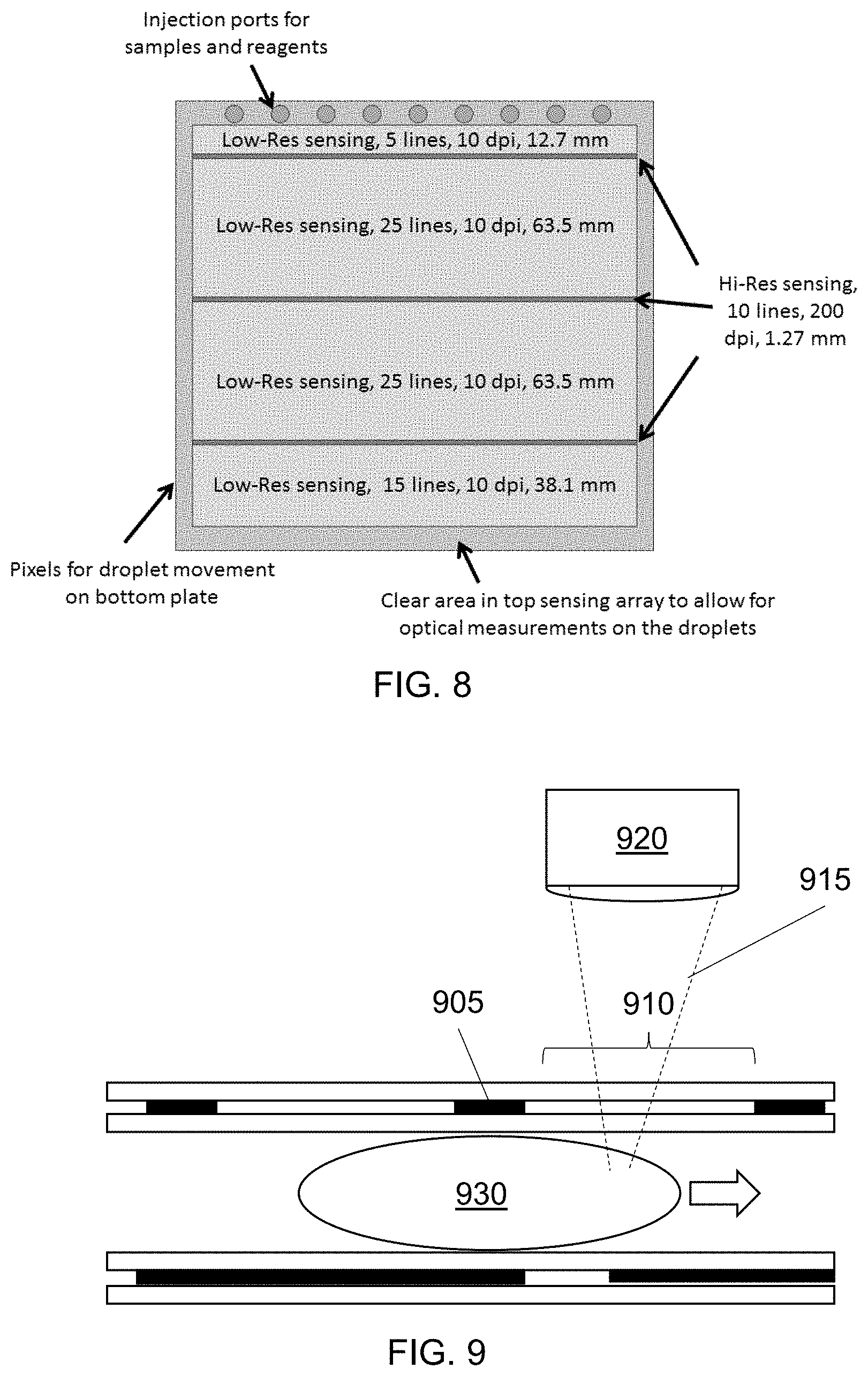
FIG. 8 illustrates a top view of a digital microfluidic device wherein the sensing electrodes are arranged with varying regions of high and low density. The electrode arrangement shown in FIG. 8 provides the necessary functionality (droplet size determination and motion tracking) for many analytical functions while reducing the complexity of the device and the cost of production;
FIG. 9 illustrates an alternate embodiment including a light-transmissive region where droplets can be interrogated with electromagnetic radiation, i.e., light. It is understood that both the probe light and the resulting signal may enter/exit through the same light-transmissive region;
FIG. 10 shows an alternative arrangement of sensing electrodes arranged with varying regions of high and low density;
FIG. 11 shows an alternative arrangement of sensing electrodes arranged with varying regions of high and low density;
FIG. 12 shows an alternative arrangement including elongated sensing electrodes arranged with varying regions of high and low density;
FIG. 13 shows an alternative arrangement including elongated sensing electrodes arranged with varying regions of high and low density.
DETAILED DESCRIPTION
As indicated above, the present invention provides an active matrix electrowetting on dielectric (AM-EWoD) device including dual substrates with thin-film transistors (TFT) and capacitive sensing. As depicted herein the "bottom" substrate includes a plurality of electrodes to propel various droplets through a microfluidic region. The "top" substrate includes a plurality of electrodes to provide a signal and to detect the presence and/or size and/or composition of a droplet with capacitive sensing. The use of "top" and "bottom" is merely a convention as the locations of the two substrates can be switched, and the devices can be oriented in a variety of ways, for example, the top and bottom plates can be roughly parallel while the overall device is oriented so that the substrates are normal to a work surface (as opposed to parallel to the work surface as shown in the figures). The top or the bottom substrate may include additional functionality, such as resistive heating and/or temperature sensing. Because the devices incorporate TFT-based sensors, the devices have much higher sensitivity and resolution than known passive devices. Additionally, because both of the electrodes needed for capacitive sensing are on the same substrate, the top and bottom electrodes do not need to be aligned, and the sensing pixels can be of different sizes or configurations as compared to the propulsion electrodes. Additionally, the designs can be implemented with amorphous silicon, thereby reducing the cost of production to the point that the devices can be disposable. It is also possible to use a-Si TFTs for the bottom plate to benefit from their higher operation voltage, and poly-Si TFTs on the top plate for higher sensitivity sensing.
The fundamental operation of an EWoD device is illustrated in the sectional image of FIG. 2. The EWoD 200 includes a cell filled with an oil 202 and at least one aqueous droplet 204. The cell gap is typically in the range 50 to 200 .mu.m, but the gap can be larger. In a basic configuration, as shown in FIG. 2, a plurality of propulsion electrodes 205 are disposed on one substrate and a singular top electrode 206 is disposed on the opposing surface. The cell additionally includes hydrophobic coatings 207 on the surfaces contacting the oil layer, as well as a dielectric layer 208 between the propulsion electrodes 205 and the hydrophobic coating 207. (The upper substrate may also include a dielectric layer, but it is not shown in FIG. 2). The hydrophobic layer prevents the droplet from wetting the surface. When no voltage differential is applied between adjacent electrodes, the droplet will maintain a spheroidal shape to minimize contact with the hydrophobic surfaces (oil and hydrophobic layer). Because the droplets do not wet the surface, they are less likely to contaminate the surface or interact with other droplets except when that behavior is desired.
While it is possible to have a single layer for both the dielectric and hydrophobic functions, such layers typically require thick inorganic layers (to prevent pinholes) with resulting low dielectric constants, thereby requiring more than 100V for droplet movement. To achieve low voltage actuation, it is better to have a thin inorganic layer for high capacitance and to be pinhole free, topped by a thin organic hydrophobic layer. With this combination it is possible to have electrowetting operation with voltages in the range +/-10 to +/-50V, which is in the range that can be supplied by conventional TFT arrays.
When a voltage differential is applied between adjacent electrodes, the voltage on one electrode attracts opposite charges in the droplet at the dielectric-to-droplet interface, and the droplet moves toward this electrode, as illustrated in FIG. 2. The voltages needed for acceptable droplet propulsion depend on the properties of the dielectric and hydrophobic layers. AC driving is used to reduce degradation of the droplets, dielectrics, and electrodes by various electrochemistries. Operational frequencies for EWoD can be in the range 100 Hz to 1 MHz, but lower frequencies of 1 kHz or lower are preferred for use with TFTs that have limited speed of operation.
As shown in FIG. 2, the top electrode 206 is a single conducting layer normally set to zero volts or a common voltage value (VCOM) to take into account offset voltages on the propulsion electrodes 205 due to capacitive kickback from the TFTs that are used to switch the voltage on the electrodes (see FIG. 3). The top electrode can also have a square wave applied to increase the voltage across the liquid. Such an arrangement allows lower propulsion voltages to be used for the TFT connected propulsion electrodes 205 because the top plate voltage 206 is additional to the voltage supplied by the TFT.
As shown in FIG. 3, an active matrix of propulsion electrodes can be arranged to be driven with data and gate (select) lines much like an active matrix in a liquid crystal display. The gate (select) lines are scanned for line-at-a time addressing, while the data lines carry the voltage to be transferred to propulsion electrodes for electrowetting operation. If no movement is needed, or if a droplet is meant to move away from a propulsion electrode, then 0V will be applied to that (non-target) propulsion electrode. If a droplet is meant to move toward a propulsion electrode, an AC voltage will be applied to that (target) propulsion electrode.
The architecture of an amorphous silicon, TFT-switched, propulsion electrode is shown in FIG. 4. The dielectric 408 must be thin enough and have a dielectric constant compatible with low voltage AC driving, such as available from conventional image controllers for LCD displays. For example, the dielectric layer may comprise a layer of approximately 20-40 nm SiO.sub.2 topped over-coated with 200-400 nm plasma-deposited silicon nitride. Alternatively, the dielectric may comprise atomic-layer-deposited Al.sub.2O.sub.3 between 2 and 100 nm thick, preferably between 20 and 60 nm thick. The TFT is constructed by creating alternating layers of differently-doped a-Si structures along with various electrode lines, with methods know to those of skill in the art. The hydrophobic layer 407 can be constructed from materials such as Teflon.RTM. AF (Sigma-Aldrich, Milwaukee, Wis.) and FlurorPel.TM. coatings from Cytonix (Beltsville, Md.), which can be spin coated over the dielectric layer 408.
In the invention, a second substrate with TFT functionality is constructed to provide capacitive sensing capabilities, and the two layers are separated with a spacer that creates a microfluidic region between the two layers. Capacitive sensing of droplets uses two electrodes, as shown in FIG. 6. Typically, an AC signal is applied to a driving electrode 506, whereby the AC signal produces a capacitively-coupled voltage on a nearby sensing electrode 505. The capacitively-coupled signal is measured by external circuitry, and changes in the signal are indicative of the material between the drive electrode 506 and the sensing electrode 505. For example, the coupled voltage will be obviously different depending on whether oil 202 or an aqueous droplet 204 is between the electrodes because of the differences in the relative permittivity between the materials. (Silicone oil has a relative permittivity of .epsilon..sub.r=2.5, ethanol has a relative permittivity of .epsilon..sub.r=24, and water has a relative permittivity of .epsilon..sub.r=80.)
The architecture of an amorphous silicon sensing layer, including TFT-switched sensing electrodes 505 and drive electrodes 506 is shown in FIG. 5. The AC signal for the driving electrodes runs horizontally and only one line at a time is activated to minimize capacitive coupling to read-out lines and "OFF" sensing electrodes. TFTs are not perfect switches and have some small conductance even in the "OFF" state. This means that a large number of OFF lines can have similar signal to one "ON" pixel. For this reason it is better to minimize capacitive signals from ac voltages above and below the row being driven by only having ac voltages on the row being driven.
As shown in FIG. 6, the sensing and drive electrodes create a coplanar gap cell. One major advantage is that the two plates do not need to be accurately aligned, or even to have the same pixel pitch, thus fabrication of a two plate system is simplified. Additional details of capacitive sensing for droplets using interdigital gap cells can be found in, e.g., "Capacitance Variation Induced by Microfluidic Two-Phase Flow across Insulated Interdigital Electrodes in Lab-On-Chip Devices", T. Dong, C Barbosa, Sensors, 15, 2694-2708, (2015), which is incorporated by reference in its entirety. The circuitry for detecting the capacitive signals may include various electrical components, including amplifiers, multiplexing switches. Advanced designs may include an array of a-Si TFTs coupled to a multi-channel charge sensor, such as used for digital x-ray imaging. See, "Front-end electronics for imaging detectors", G. De Geronimo, et al., Nuclear Instruments and Methods in Physics Research A, 471 pp. 192-199, (2001), which is incorporated by reference in its entirety.
In some embodiments, it is unnecessary to provide multiple independent drive electrodes for the AC signal. As shown in FIG. 7, the drive electrode can be arranged to be contiguous, but interdigitated with the sensing electrodes. (All of the electrodes shown in FIG. 7 are in the same metal layer, but are shown in different colors to signify their function.) In FIG. 7, the AC signal is provided to a singular driving electrode that runs horizontally across the surface, while various sensing electrodes are "read" across the array. Typically, only one sensor line at a time is activated to minimize capacitive coupling between the AC signal from the driving electrode and sensing electrodes that are in the "OFF" mode. Without such line-by-line readout, the signal from the numerous sensing electrodes with a "null" state (e.g., coupled to oil) will appear larger than proper, decreasing the signal-to-noise of the correctly sensing electrodes. In an alternative embodiment, the top substrate may include drive electrodes, sensing electrodes, and an earthed grid. The drive and sensing electrodes can be used for droplet sensing, as described above, while the earthed grid provides an electrode surface area opposite the propulsion electrode that has low impedance to electrical ground.
The invention will use circuits coupled to the top drive and sensing electrodes to provide capacitive sensing, thereby allowing the device to track the position of droplets manipulated by the device. However, the signal from capacitive sensing of droplets over a small sensing electrode is also relatively small, thus one to three hundred lines of sensor electrodes may be needed to obtain acceptable signal-to-noise ratios. Providing such a high density of sensing electrodes across the entire device would be expensive and unnecessary. Thus, for larger arrays (such as for combinatorial chemistry) it is preferred to have small localized areas with high densities of sensing pixels on the top plate for particle sizing, with lower density elsewhere for movement sensing.
As shown in FIG. 8, an AM-EWoD device can be created with differing densities of sensing electrodes at various locations on the top plate. In the embodiment of FIG. 8, there are 200 dpi high-resolution areas on the array for droplet size measurement, and 10 dpi resolution areas to track droplet movement. In FIG. 8, the sensor would be 181.61 mm wide for 100 measurement lines. If the TFT EWoD propulsion substrate below the sensing plate had a uniform resolution of 200 dpi (electrodes per inch) then there would be 1430 rows of propulsion electrodes for controlling movement, mixing, etc. of droplets. In contrast, a device limited to one hundred sensing rows with a resolution of 180 dpi across the entire device would only be 14.1 mm wide, resulting in only 111 rows of propulsion electrodes; likely too small for complex assays. Thus, by providing differing densities a larger device can be produced with all of the needed sensing capability. In general, a low-resolution area will include between 1 and 15 electrodes per linear centimeter, while a high-resolution area will include between 20 and 200 electrodes per linear centimeter. Typically, the total area (length.times.width) of sensing electrodes with the lower density (a.k.a., "low-res") is greater than the total area of sensing electrodes with the higher density (a.k.a., "high-res"). For example, there could be three times or greater of the low-res area as compared to the high-res area s compared to the high-res area. For example, there could be five times or greater of the low-res area. For example, there could be ten times or greater of the low-res area as compared to the high-res area.
An additional benefit of using different densities of sensing electrodes is that portions of the top plate can be provided with transparent, or otherwise light-transmissive, areas to allow further interrogation of droplets. For example, fluorescent markers may be observed by illuminating a droplet through the top substrate with a light source and then using a detector and optionally color filters to observe the resulting fluorescence through the top substrate. In other embodiments, the light may pass through both the top and bottom substrates to allow absorption measurements in the IR, UV, or visible wavelengths. Alternatively, attenuated (frustrated) total-internal reflection spectroscopy can be used to probe the contents and or location of droplets in the system.
An embodiment of such a system is shown in FIG. 9, wherein a gap 910 between sensing electrodes 905 is on the order of 2 mm, allowing light 915 to pass from an objective 920 to illuminate a passing droplet 930. In an embodiment, the droplet 930 includes fluorescent molecules, and the resulting fluorescent signal is collected back through the objective 920 and split using a dichroic filter (not shown) to be detected with a detector (not shown). Thus, the design allows different types of information, e.g., both capacitive and spectroscopic, to be collected on droplets as they move through the system.
As discussed with respect to FIG. 8, the simplest way for implementing low resolution sensing would be to have the same sensing pixel design as the high-resolution areas, but have large spaces around the sensing pixel. This concept is illustrated in a different embodiment in FIG. 10. Using the design of FIG. 10, it would be possible for droplets to pass between the low resolution sensing pixels, but a droplet control algorithm could be written to ensure droplets pass over the sensing pixels on a regular basis, allowing the size and composition of the droplets to be monitored. As illustrated in FIG. 10, a uniform distribution of low resolution pixels makes it possible to dramatically increase the area over which sensing is available, while at the same time allowing the use of commercially-available drivers. As an alternative, the number of sensing pixels on any one vertical sensing line can be constant, while the sensing pixels are staggered, as shown in FIG. 11. Other patterns, such as pseudo-random may also be employed to maximize the interaction with the droplets, while reducing the actual number of sensing TFTs that must be fabricated and later addressed.
It is also possible to create low-resolution and high-resolution sensing areas using differently shaped electrodes, as shown in FIGS. 12 and 13. FIG. 12 shows square pixels in the high resolution sensing area and larger rectangular sensing pixels in the low resolution sensing area. This design would be efficient for sensing movement up and down the array, i.e., moving from one elongated electrode to another. This same technique could be implemented to make both horizontal and vertical elongated electrodes that would provide droplet tracking with lower resolution. FIG. 13 shows low resolution area with vertical and horizontal rectangular sensing pixels to detect vertical and horizontal movement of droplets. Other geometric designs, such as spirals can also be used to facilitate location sensing with fewer electrodes and fewer TFTs. As shown in FIGS. 12 and 13, the droplets can be easily moved from the low density regions, where droplet creation, splitting, or mixing take place, to high density regions where size and composition of those droplets can be evaluated.
From the foregoing, it will be seen that the present invention can provide low-cost lab-on-a-chip functionality. In particular, by using the described architecture, an electrowetting on dielectric system can be created using amorphous-silicon fabrication facilities and lower cost driving electronics. The invention makes efficient use of the available surfaces on both the top and the bottom of the EWoD device, but does not require alignment of the electrodes on the top and bottom surfaces.
It will be apparent to those skilled in the art that numerous changes and modifications can be made in the specific embodiments of the invention described above without departing from the scope of the invention. Accordingly, the whole of the foregoing description is to be interpreted in an illustrative and not in a limitative sense.
* * * * *
D00000
D00001
D00002
D00003
D00004
D00005
D00006
D00007
XML
uspto.report is an independent third-party trademark research tool that is not affiliated, endorsed, or sponsored by the United States Patent and Trademark Office (USPTO) or any other governmental organization. The information provided by uspto.report is based on publicly available data at the time of writing and is intended for informational purposes only.
While we strive to provide accurate and up-to-date information, we do not guarantee the accuracy, completeness, reliability, or suitability of the information displayed on this site. The use of this site is at your own risk. Any reliance you place on such information is therefore strictly at your own risk.
All official trademark data, including owner information, should be verified by visiting the official USPTO website at www.uspto.gov. This site is not intended to replace professional legal advice and should not be used as a substitute for consulting with a legal professional who is knowledgeable about trademark law.