Enhanced HFET
Wang , et al. December 1, 2
U.S. patent number 10,854,741 [Application Number 16/610,207] was granted by the patent office on 2020-12-01 for enhanced hfet. This patent grant is currently assigned to THE 13TH RESEARCH INSTITUTE OF CHINA ELECTRONICS. The grantee listed for this patent is THE 13TH RESEARCH INSTITUTE OF CHINA ELECTRONICS TECHNOLOGY GROUP CORPORATION. Invention is credited to Shujun Cai, Yulong Fang, Zhihong Feng, Guodong Gu, Hongyu Guo, Yuanjie Lv, Xubo Song, Xin Tan, Yuangang Wang, Xingye Zhou.

| United States Patent | 10,854,741 |
| Wang , et al. | December 1, 2020 |
Enhanced HFET
Abstract
An enhanced HFET, comprising a HFET device body. Regions without two-dimensional electron gas are provided on a channel layer (2) at the portion between a drain electrode (6) and a source electrode (4) of the HFET device body, and there is a region without two-dimensional electron gas provided on the channel layer (2) at the portions excluding the area under a gate electrode (5); two-dimensional electron gas regions are provided on the channel layer (2) excluding the portions located between the drain electrode (6) and the source electrode (4) and provided with the regions without two-dimensional electron gas; the channel layer (2) at the portion between the gate electrode (5) and the source electrode (4) and the portion between the gate electrode (5) and the drain electrode (6) are each provided with a two-dimensional electron gas region; and two-dimensional electron gas (8) is provided at a portion or whole portion of a two-dimensional electron gas layer at the channel layer (2) at the portion right under the gate electrode (5). The HFET has the advantages of high saturation current, high threshold voltage controllability, fast response, low energy consumption, and the like.
| Inventors: | Wang; Yuangang (Shijiazhuang, CN), Feng; Zhihong (Shijiazhuang, CN), Lv; Yuanjie (Shijiazhuang, CN), Tan; Xin (Shijiazhuang, CN), Song; Xubo (Shijiazhuang, CN), Zhou; Xingye (Shijiazhuang, CN), Fang; Yulong (Shijiazhuang, CN), Gu; Guodong (Shijiazhuang, CN), Guo; Hongyu (Shijiazhuang, CN), Cai; Shujun (Shijiazhuang, CN) | ||||||||||
|---|---|---|---|---|---|---|---|---|---|---|---|
| Applicant: |
|
||||||||||
| Assignee: | THE 13TH RESEARCH INSTITUTE OF
CHINA ELECTRONICS (Hebei, CN) |
||||||||||
| Family ID: | 1000005217037 | ||||||||||
| Appl. No.: | 16/610,207 | ||||||||||
| Filed: | December 11, 2017 | ||||||||||
| PCT Filed: | December 11, 2017 | ||||||||||
| PCT No.: | PCT/CN2017/115427 | ||||||||||
| 371(c)(1),(2),(4) Date: | November 01, 2019 | ||||||||||
| PCT Pub. No.: | WO2018/201721 | ||||||||||
| PCT Pub. Date: | November 08, 2018 |
Prior Publication Data
| Document Identifier | Publication Date | |
|---|---|---|
| US 20200075754 A1 | Mar 5, 2020 | |
Foreign Application Priority Data
| May 4, 2017 [CN] | 2017 1 0308243 | |||
| Current U.S. Class: | 1/1 |
| Current CPC Class: | H01L 29/7786 (20130101); H01L 29/42316 (20130101) |
| Current International Class: | H01L 29/778 (20060101); H01L 29/423 (20060101) |
| Field of Search: | ;257/194 |
References Cited [Referenced By]
U.S. Patent Documents
| 8937338 | January 2015 | Chowdhury |
| 10270436 | April 2019 | Chen |
| 10741682 | August 2020 | Jeon |
| 2011/0121314 | May 2011 | Suh |
| 2016/0087089 | March 2016 | Prechtl et al. |
| 2017/0338810 | November 2017 | Chen |
| 2018/0254326 | September 2018 | Dong |
| 101252088 | Aug 2008 | CN | |||
| 101969071 | Feb 2011 | CN | |||
| 102130160 | Jul 2011 | CN | |||
| 103715256 | Apr 2014 | CN | |||
| 104538440 | Apr 2015 | CN | |||
| 106531789 | Mar 2017 | CN | |||
| 206116406 | Apr 2017 | CN | |||
| 107093629 | Aug 2017 | CN | |||
Other References
|
International Search Report and English translation of the International Search Report in the international application No. PCT/CN2017/115427, dated Mar. 16, 2018, 6 pages. cited by applicant . Written Opinion and English translation of the Written Opinion of the International Search Authority in the international application No. PCT/CN2017/115427, dated Mar. 16, 2018, 9 pages. cited by applicant . Cai, et al., "High-Performance Enhancement-Mode AIGaN/GaN HFETs Using Fluoride-Based Plasma Treatment", IEEE Electron Device Letters, 2005, 26(7), pp. 435-437, 4 pages. cited by applicant . Development and Characteristic Analysis of Enhancement-mode AlGaN/GaN Trench HFET, Yue Hao, Chong Wang, Jinyu Ni, Qian Feng, Jincheng Zhang, and Wei Mao, Science in China Series E, 39 (1). 2009, pp. 119-123, in which, a threshold voltage of a device is boosted from -2.2V to 0.47V with a technology of grooving under a gate, 6 pages. cited by applicant . Simulation Model Development and Verification for High Voltage GaN HFET in Cascode Structure. Energy Conversion Congress and Exposition, Zhengyang Liu, Xiucheng Huang, Fred C. Lee, and Qiang Li. ECCE, IEEE, 2013, pp. 3537-3594, in which an enhancement-mode Cascode GaN HFET is disclosed, a threshold of the GaN HFET is controlled by means of a Si device in the structure, 9 pages. cited by applicant. |
Primary Examiner: Anya; Igwe U
Attorney, Agent or Firm: Cooper Legal Group, LLC
Claims
The invention claimed is:
1. An enhancement-mode hetero-structure field effect transistor (HFET), comprising a HFET device body, wherein a region without two-dimensional electron gas is provided on a channel layer between a drain electrode and a source electrode of the HFET device body, the region without two-dimensional electron gas is provided on the channel layer except an area under a gate electrode, regions with two-dimensional electron gas are provided on the channel layer, except the region without two-dimensional electron gas, between the drain electrode and the source electrode, the regions with two-dimensional electron gas are provided on both the channel layer between the gate electrode and the source electrode and the channel layer between the gate electrode and the drain electrode, respectively, and the channel layer right under the gate electrode is partially or all provided with two-dimensional electron gas at a two-dimensional electron gas layer.
2. The enhancement-mode HFET of claim 1, wherein a number of regions without two-dimensional electron gas is more than one.
3. The enhancement-mode HFET of claim 1, wherein a width range of each region without two-dimensional electron gas is greater than or equal to 1 nm and less than or equal to 10 .mu.m.
4. The enhancement-mode HFET of claim 3, wherein the width range of each region without two-dimensional electron gas is greater than or equal to 50 nm and less than or equal to 800 nm.
5. The enhanced HFET of claim 1, wherein a number of gate electrodes is an integer more than or equal to 1.
6. The enhancement-mode HFET of claim 1, wherein a number of gate electrodes is an integer more than 1, and the gate electrodes have a same length or different lengths.
7. The enhancement-mode HFET of claim 1, wherein the gate electrode is one or a combination of a straight gate, a T-shaped gate, a TT-shaped gate, a TTT-shaped gate, a V-shaped gate, a U-shaped gate and a Y-shaped gate.
8. The enhancement-mode HFET of claim 1, wherein when one gate electrode is provided on the HFET device body, an insulating medium layer is provided between a gate root at a lower side of the gate electrode and a barrier layer; or no insulating medium layer is provided between a gate root at a lower side of the gate electrode and a barrier layer, and when more than two gate electrodes are provided on the HFET device body, an insulating medium layer is provided between a gate root at a lower side of a part of the gate electrodes and a barrier layer, or no insulating medium layer is provided between the gate root at the lower side of the part of the gate electrodes and the barrier layer; or an insulating medium layer is provided between a gate root at a lower side of all of the gate electrodes and a barrier layer, or, no insulating medium layer is provided between the gate root at the lower side of all of the gate electrodes and the barrier layer.
9. The enhancement-mode HFET of claim 1, wherein the HFET device body comprises a substrate, the channel layer is provided on an upper surface of the substrate, the source electrode, is provided at a left side of an upper surface of the channel layer, the drain electrode is provided at a right side of the upper surface of the channel layer, a barrier layer is provided on the upper surface, between the source electrode and the drain electrode, of the channel layer, more than one gate electrode is provided on an upper surface of the barrier layer, a passivation layer is provided on the upper surface, except an area where the gate electrode is arranged, of the barrier layer, an insulating medium layer is provided between a gate root at a lower side of the gate electrode and the barrier layer, or no insulating medium layer is provided between a gate root at a lower side of the gate electrode and the barrier layer.
10. The enhancement-mode HFET of claim 9, wherein a part of the upper surface of the barrier layer is further provided with a P-type cap layer, which is used for forming the region without two-dimensional electron gas.
Description
TECHNICAL FIELD
The disclosure relates to the technical field of semiconductor switch devices, in particular to an enhancement-mode hetero-structure field effect transistor (HFET).
BACKGROUND
Reference 1: High-Performance Enhancement-Mode AlGaN/GaN HFETs Using Fluoride-Based Plasma Treatment. IEEE Electron Device Letters, Yong Cai, Yugang Zhou, Kevin J. Chen, and Kei May Lau., 2005, 26(7), pp. 435-437, in which, a threshold voltage of a device is transferred by adopting F plasma treatment, the threshold voltage of the device is boosted from -4V to 0.9V, and an enhancement-mode device is implemented.
Reference 2: Development and Characteristic Analysis of Enhancement-mode AlGaN/GaN Trench HFET, Yue Hao, Chong Wang, Jinyu Ni, Qian Feng, Jincheng Zhang, and Wei Mao, Science in China Series E, 39 (1), 2009, pp. 119-123, in which, a threshold voltage of a device is boosted from -2.2V to 0.47V with a technology of grooving under a gate.
Reference 3: Simulation Model Development and Verification for High Voltage GaN HFET in Cascode Structure. Energy Conversion Congress and Exposition, Zhengyang Liu, Xiucheng Huang, Fred C. Lee, and Qiang Li. ECCE, IEEE, 2013, pp. 3587-3594, in which an enhancement-mode Cascode GaN HFET is disclosed, a threshold of the GaN HFET is controlled by means of a Si device in the structure.
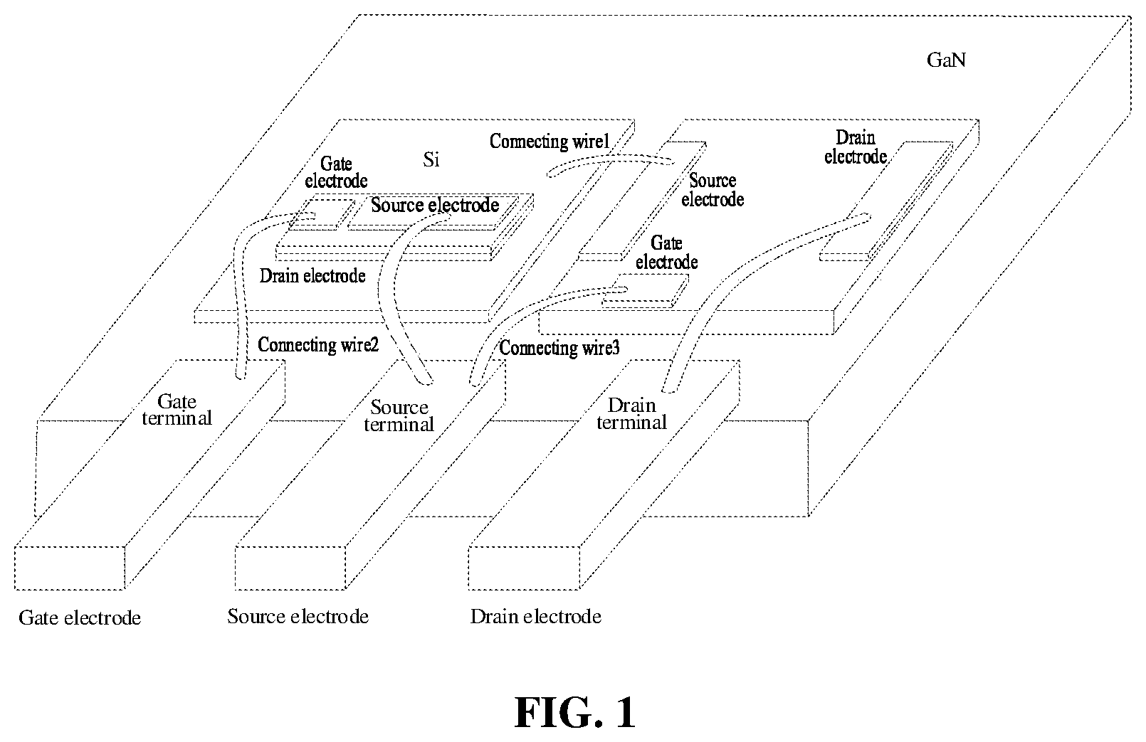
At present, all the enhancement-mode HFETs based on Group III nitride materials adopt a planar channel layer, and the enhancement is implemented by grooving, injecting F plasmas and cascading with the Si device (as illustrated in FIG. 1). The grooving process causes a large damage to a gate interface. The grooving process without damage is difficult to implemented, and the threshold changes significantly with the depth of the groove. The injection of F plasmas is instable, and the switch characteristic of a cascade structure is limited by the Si device.
SUMMARY
Technical Problems
The technical problem to be solved by the disclosure is how to provide an enhancement-mode HFET with high saturation current and a controllable enhancement threshold.
Technical Solutions
To solve the above technical problem, the technical solution adopted by the disclosure is an enhancement-mode HFET, which includes a HFET device body. A region without two-dimensional electron gas is provided on a channel layer between a drain electrode and a source electrode of the HFET device body, and the region without two-dimensional electron gas is provided on the channel layer except the area under a gate electrode. Regions with two-dimensional electron gas is provided on the channel layer, except the region without two-dimensional electron gas, between the drain electrode and the source electrode, and regions with the two-dimensional electron gas are provided on both the channel layer between the gate electrode and the source electrode and the channel layer between the gate electrode and the drain electrode. The channel layer right under the gate electrode is partially or all provided with two-dimensional electron gas at a two-dimensional electron gas layer.
In a further technical solution, the number of regions without two-dimensional electron gas is more than one.
In a further technical solution, a width range of each region without two-dimensional electron gas is greater than or equal to 1 nm and less than or equal to 10 .mu.m.
In a further technical solution, a width range of each region without two-dimensional electron gas is greater than or equal to 50 nm and less than or equal to 800 nm.
In a further technical solution, the number of the gate electrodes is an integer more than or equal to 1.
In a further technical solution, the number of the gate electrodes is an integer more than 1, and the gate electrodes have a same length or different lengths.
In a further technical solution, the gate electrodes are one or a combination of a straight gate, a T-shaped gate, a TT-shaped gate, a TTT-shaped gate, a V-shaped gate, a U-shaped gate and a Y-shaped gate.
In a further technical solution, when one gate electrode is provided on the HFET device, an insulating medium layer is provided between a gate root at the lower side of the gate electrode and a barrier layer, or no insulating medium layer is provided between a gate root at the lower side of the gate electrode and a barrier layer. When more than two gate electrodes are provided on the HFET device, an insulating medium layer is provided between the gate root at the lower side of a part of the gate electrodes and the barrier layer, and no insulating medium layer is provided between the gate root at the lower side of a part of the gate electrodes and the barrier layer. Alternatively, an insulating medium layer is provided between the gate root at the lower side of all of the gate electrodes and the barrier layer, or, no insulating medium layer is provided between the gate root at the lower side of all of the gate electrodes and the barrier layer.
In a further technical solution, the HFET device body includes a substrate. A channel layer is provided on an upper surface of the substrate layer, a source electrode is provided at a left side of the upper surface of the channel layer, and a drain electrode is provided at a right side of the upper surface of the channel layer. A barrier layer is provided on the upper surface, between the source electrode and the drain electrode, of the channel layer. More than one gate electrodes are provided on the upper surface of the barrier layer. A passivation layer is provided on the upper surface, except a region where the gate electrode is arranged, of the barrier layer. An insulating medium layer is provided between a gate root at a lower side of the gate electrode and the barrier layer, or no insulating medium layer is provided between a gate root at a lower side of the gate electrode and the barrier layer.
In a further technical solution, a part of the upper surface of the barrier layer is further provided with a P-type cap layer, which is used for forming the region without two-dimensional electron gas.
Beneficial effects of the disclosure
The beneficial effects generated by adopting the above technical solutions include the followings. A region without two-dimensional electron gas is provided on a channel layer between a drain electrode and a source electrode of the HI-BT device body, and the region without two-dimensional electron gas is a two-dimensional electron gas barrier region. As a forward voltage of the gate electrode increases, the barrier width and height decrease continuously. When the device is switched on, electron tunneling may happen in the region without two-dimensional electron gas (2DEG), and the saturation current is high. The barrier height of the region without 2DEG has a small influence on the threshold voltage of the device, which improve controllability for the threshold. Due to the controllable threshold, the device can be applied to a power electronic device and a digital circuit, so as to improve the speed and reduce power consumption. The device may be switched on or off only by controlling a small amount of electrons of the region without 2DEG to charge or discharge, which improves a switching speed. When the device is switched on, the width of the region without 2DEG has a great influence on the threshold voltage, and a threshold voltage can be controllable in an ultra-wide range.
BRIEF DESCRIPTION OF DRAWINGS
FIG. 1 is a three-dimensional schematic structural diagram of a Cascode GaN HFET in the conventional art.
FIG. 2 is a schematic structural diagram of an enhancement-mode HFET according to the first embodiment of the disclosure.
FIG. 3 is a schematic structural diagram of an enhancement-mode single-gate GaN HFET prepared by a fluorine treatment process according to the second embodiment of the disclosure.
FIG. 4 is a schematic structural diagram of a groove enhancement-mode dual-gate GaN HFET according to the third embodiment of the disclosure.
FIG. 5 is a schematic structural diagram of a groove enhancement-mode dual-gate GaN HFET according to the fourth embodiment of the disclosure.
FIG. 6 is a schematic structural diagram of a groove enhancement-mode tri-gate GaN HFET according to the fifth embodiment of the disclosure.
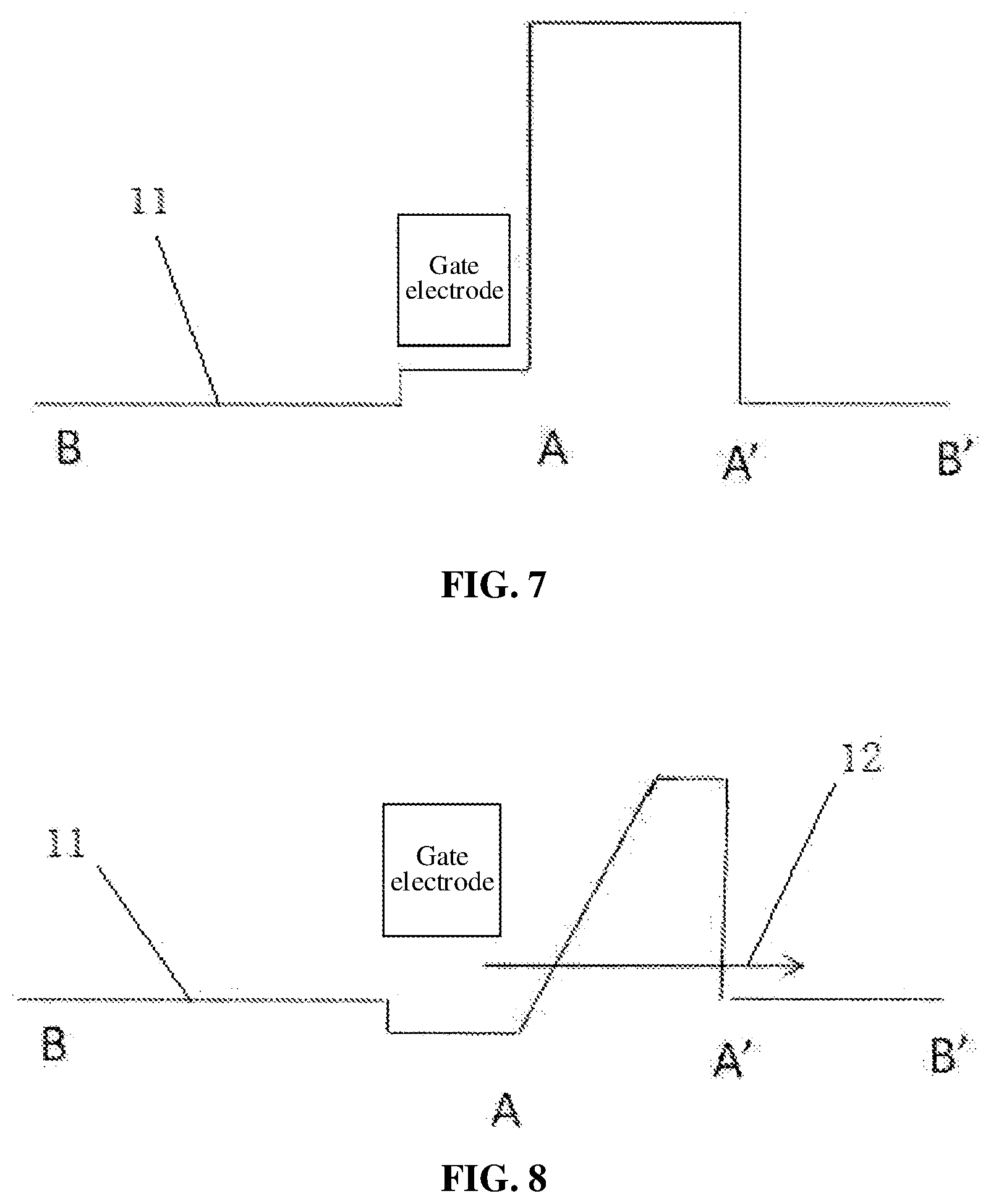
FIG. 7 is a schematic diagram of a conduction band at the interface of a barrier layer/a channel layer when a gate voltage of the enhancement-mode HFET is equal to 0V according to the first embodiment of the disclosure.
FIG. 8 is a schematic diagram of the conduction band at the interface of the barrier layer/the channel layer when the gate voltage of the enhancement-mode HFET is greater than a threshold voltage which is greater than 0V according to the first embodiment of the disclosure.
Here, 1 represents a barrier layer; 2 represents a channel layer; 3 represents a substrate; 4 represents a source electrode; 5 represents a gate electrode; 6 represents a drain electrode; 7 represents a passivation layer; 8 represents two-dimensional electron gas; 9 represents an insulating medium layer; 10 represents a P-type cap layer; 11 represents a conduction band; and 12 represents electron tunneling.
DETAILED DESCRIPTION
The technical solutions of the disclosure are described clearly and completely below in combination with the drawings. Apparently, the described embodiments are merely a part, rather than all, of the embodiments of the disclosure. On the basis of the embodiments of the disclosure, all other embodiments obtained by those skilled in the art without creative work fall within the protection scope of the disclosure.
A lot of details are described in the following description to fully understand the disclosure, but the disclosure may also be implemented by other ways different from that described here. Those skilled in the art may make the similar promotions without departing from the connotation of the disclosure, and the disclosure is not limited to the specific embodiments disclosed below.
First Embodiment
As illustrated in FIG. 2, the embodiments of the present disclosure provide an enhancement-mode HFET, which includes a HFET device body. The HFET device body includes a substrate 1. A channel layer 2 is provided on an upper surface of the substrate 1. A source electrode 4 is provided at the left side of an upper surface of the channel layer 2. A drain electrode 6 is provided at the right side of the upper surface of the channel layer 2. A barrier layer 1 is provided on an upper surface, between the source electrode 4 and the drain electrode 6, of the channel layer, and a two-dimensional electron gas (2DEG) layer is formed on the channel layer 2 below the barrier layer 1. A region (a region from A to A' in FIG. 2) without two-dimensional electron gas is provided on the channel layer 2 between the drain electrode 6 and the source electrode 4, and a region with two-dimensional electron gas is provided on the channel layer 2, except the region without two-dimensional electron gas, between the drain electrode 6 and the source electrode 4. That is, the two-dimensional electron gas layer is discontinuous, and is divided into two regions (the region from B to A and the region from A' to B' in FIG. 2) with two-dimensional electron gas including a left region with two-dimensional electron gas and a right region with two-dimensional electron gas by the region without two-dimensional electron gas. A gate electrode 5 is provided on an upper surface of the barrier layer. The gate electrode 5 is a T-type gate. A passivation layer 7 is provided on the upper surface, except a region where the gate electrode 5 is arranged, of the barrier layer 1. The channel layer right under the gate electrode 5 is provided with two-dimensional electron gas at the two-dimensional electron gas layer.
The region without two-dimensional electron gas is provided on the channel layer between the drain electrode and the source electrode of the HFET device body, and the region is the two-dimensional electron gas barrier region. As a forward voltage of the gate electrode increases, the barrier width and height decrease continuously. When the device is switched on, electron tunneling may happen in the region without two-dimensional electron gas (2DEG), and the saturation current is high. The barrier height of the region without 2DEG has a small influence on the threshold voltage of the device, which improve controllability for the threshold. Due to the controllable threshold, the device can be applied to a power electronic device and a digital circuit, so as to improve the speed and reduce power consumption. The device may be switched on or off only by controlling a small amount of electrons of the region without 2DEG to charge or discharge, which improve a switching speed. When the device is switched on, the width of the region without 2DEG has a great influence on the threshold voltage, and a threshold voltage can be controllable in an ultra-wide range.
FIG. 7 is a schematic diagram of a conduction band at the interface of the barrier layer/the channel layer when a gate voltage of the enhancement-mode HFET is equal to 0V according to the first embodiment of the disclosure. FIG. 8 is a schematic diagram of the conduction band at the interface of the barrier layer/the channel layer when the gate voltage of the enhancement-mode HFET is greater than a threshold voltage which is greater than 0V according to the first embodiment of the disclosure. The barrier height and width decrease with the increase of a positive gate voltage, and a possibility of the electronic tunneling increases with the decrease of the barrier height and width.
Second Embodiment
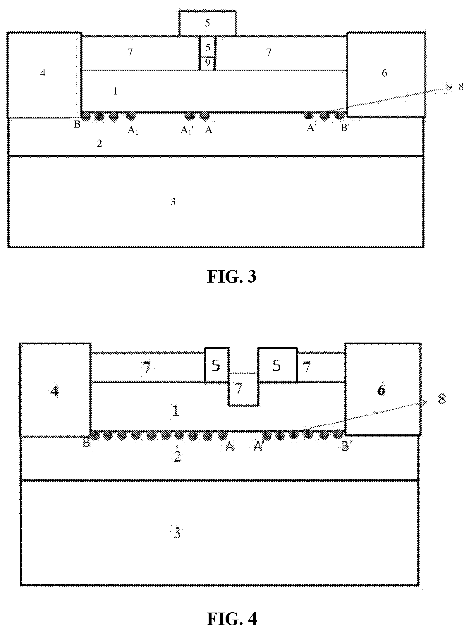
As illustrated in FIG. 3, the embodiments of the present disclosure provide an enhancement-mode HFET, which includes a HFET device body. The HFET device body includes a substrate 1. A channel layer 2 is provided on an upper surface of the substrate 1. A source electrode 4 is provided at the left side of the upper surface of the channel layer 2. A drain electrode 6 is provided at the right side of the upper surface of the channel layer 2. A barrier layer 1 is provided on an upper surface, between the source electrode 4 and the drain electrode 6, of the channel layer, and a two-dimensional electron gas (2DEG) layer is formed on the channel layer 2 below the barrier layer 1. Two regions (the region from A.sub.1 to A.sub.1' and the region from A to A' in FIG. 3) without two-dimensional electron gas are provided on the channel layer 2 between the drain electrode 6 and the source electrode 4. The region without 2DEG is formed by injecting fluorine ions.
A region with two-dimensional electron gas is provided on the channel layer 2, except the region without two-dimensional electron gas, between the drain electrode 6 and the source electrode 4. That is, the two-dimensional electron gas layer is discontinuous, and is divided into three regions (the region from B to A.sub.1, the region from A.sub.1' to A, and the region from A' to B' in FIG. 3) with two-dimensional electron gas by the region without two-dimensional electron gas. An insulating medium layer 9 is provided on a part of the upper surface of the barrier layer. A T-type gate electrode is provided on the upper surface of the insulating medium layer 9. A passivation layer 7 is provided on the upper surface, except a region where the gate electrode 5 is arranged, of the barrier layer 1. The channel layer right under the gate electrode 5 is all provided with the two-dimensional electron gas at the two-dimensional electron gas layer.
Third Embodiment
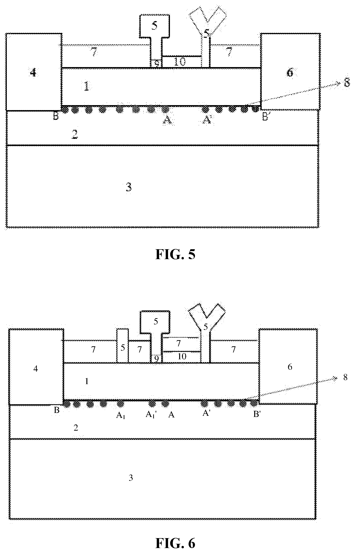
As illustrated in FIG. 4, the embodiments of the present disclosure provide an enhancement-mode HFET, which includes a HFET device body. The HFET device body includes a substrate 1. A channel layer 2 is provided on an upper surface of the substrate 1. A source electrode 4 is provided at the left side of the upper surface of the channel layer 2. A drain electrode 6 is provided at the right side of the upper surface of the channel layer 2. A barrier layer 1 is provided on the upper surface, between the source electrode 4 and the drain electrode 6, of the channel layer, and a two-dimensional electron gas (2DEG) layer is formed on the channel layer 2 below the barrier layer 1. One region (a region from A to A' in FIG. 4) without two-dimensional electron gas is provided on the channel layer 2 between the drain electrode 6 and the source electrode 4. The region without 2DEG is formed by etching the barrier layer 1.
A region with two-dimensional electron gas is provided on the channel layer 2, except the region without two-dimensional electron gas, between the drain electrode 6 and the source electrode 4. That is, the two-dimensional electron gas layer is discontinuous, and is divided into two regions (the region from B to A and the region from A' to B' in FIG. 4) with two-dimensional electron gas by the region without two-dimensional electron gas. Two gate electrodes 5 are provided on a part of the upper surface of the barrier layer 1. The gate electrodes 5 are straight gates, and have different widths. A passivation layer 7 is provided on the upper surface, except a region where the gate electrodes 5 are arranged, of the barrier layer 1, and the passivation layer 7 between the gate electrode 5 and the gate electrode 5 is embedded in the etched groove of the barrier layer 1. The channel layer right under the gate electrode 5 is provided with the two-dimensional electron gas at the two-dimensional electron gas layer.
Fourth Embodiment
As illustrated in FIG. 5, the embodiments of the present disclosure provide an enhancement-mode HFET, which includes a HFET device body. The HFET device body includes a substrate 1. A channel layer 2 is provided on an upper surface of the substrate 1. A source electrode 4 is provided at the left side of the upper surface of the channel layer 2. A drain electrode 6 is provided at the right side of the upper surface of the channel layer 2. A barrier layer 1 is provided on the upper surface, between the source electrode 4 and the drain electrode 6, of the channel layer, and a two-dimensional electron gas (2DEG) layer is formed on the channel layer 2 below the barrier layer 1. A region (the region from A to A' in FIG. 5) without two-dimensional electron gas is provided on the channel layer 2 between the drain electrode 6 and the source electrode 4. The region without 2DEG is formed by self-exhaustion of the P-type cap layer 10.
A region with two-dimensional electron gas is provided on the channel layer 2, except the region without two-dimensional electron gas, between the drain electrode 6 and the source electrode 4. That is, the two-dimensional electron gas layer is discontinuous, and is divided into two regions (the region from B to A and the region from A' to B' in FIG. 5) with two-dimensional electron gas by the region without two-dimensional electron gas. Two gate electrodes 5 are provided on a part of the upper surface of the barrier layer 1. The gate electrodes 5 are a T-type or Y-type gate. The P-type cap layer 10 is provided on the upper surface of the barrier layer 1 between two gate electrodes 5. A passivation layer 7 is provided on the upper surface, except a region between the two gate electrodes 5, of the barrier layer 1. The channel layer right under one of the two gate electrodes 5 is all provided with the two-dimensional electron gas at the two-dimensional electron gas layer, and the channel layer right under the other gate electrode 5 is partially provided with the two-dimensional electron gas at the two-dimensional electron gas layer.
Fifth Embodiment
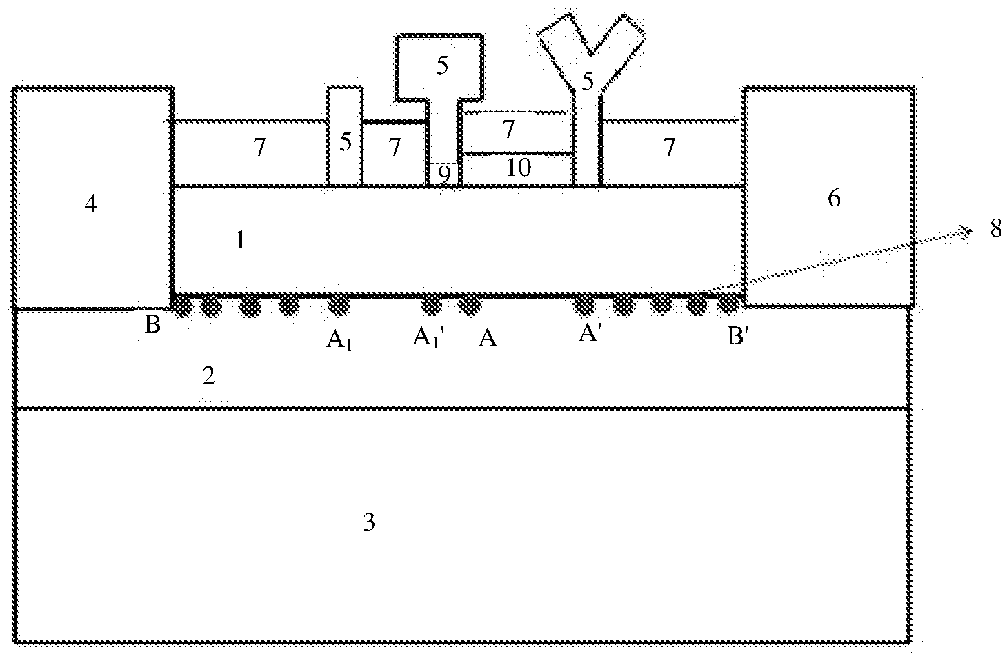
As illustrated in FIG. 6, the embodiments of the present disclosure provide an enhancement-mode HFET, which includes a HFET device body. The HFET device body includes a substrate 1. A channel layer 2 is provided on an upper surface of the substrate 1. A source electrode 4 is provided at the left side of the upper surface of the channel layer 2. A drain electrode 6 is provided at the right side of the upper surface of the channel layer 2. A barrier layer 1 is provided on the upper surface, between the source electrode 4 and the drain electrode 6, of the channel layer, and a two-dimensional electron gas (2DEG) layer is formed on the channel layer 2 below the barrier layer 1. Two regions (the region from A.sub.1 to A.sub.1' and the region from A to A' in FIG. 6) without two-dimensional electron gas are provided on the channel layer 2 between the drain electrode 6 and the source electrode 4. The two regions without two-dimensional electron gas are formed in different ways. The region from A to A' is formed by self-exhaustion of the P-type cap layer 10, and the region from A.sub.1 to A.sub.1' is formed by processing the fluorine ions.
The region with two-dimensional electron gas is provided on the channel layer 2, except the regions without two-dimensional electron gas, between the drain electrode 6 and the source electrode 4. That is, the two-dimensional electron gas layer is discontinuous, and is divided into three regions (the region from B to A.sub.1, the region from A.sub.1' to A, and the region from A' to B' in FIG. 6) with two-dimensional electron gas by the regions without two-dimensional electron gas. Two gate electrodes 5, an insulating medium layer 9 and a P-type cap layer 10 are provided on a part of the upper surface of the barrier layer 1. One gate electrode 5 is provided on the upper surface of the insulating medium layer 9. The three gate electrodes are respectively a straight gate, a T-type gate and a Y-type gate. Passivation layers are provided on the upper surface, except the regions where the gate electrodes 5 are arranged, of the barrier layer 1 and the upper surface of the P-type cap layer 10. The channel layer right under the gate electrode 5 is all provided with the two-dimensional electron gas at the two-dimensional electron gas layer.
It is to be noted that in the first embodiments to the fifth embodiment, the width range of each region without 2DEG is greater than or equal to 1 nm and less than or equal to 10 .mu.m, and a preferable range is greater than or equal to 50 nm and less than or equal to 800 nm. Moreover, according to the description of the above embodiments, those skilled in the art may also make some apparent changes. For example, the region without 2DEG is formed in other ways except the ways presented in the disclosure. The barrier layer 1 is made of one-layer or multilayer composite material. The channel layer 2 is made of the multilayer composite material, and is in structures of back barrier, multilayer buffer, and so on. The substrate is made of SiC, Si, diamond, sapphire, GaN, and so on, or is made of multilayer composite material. An epitaxial layer directly extends to the substrate or is transferred to other substrates. The gate is in the shapes except that presented in the disclosure, and the insulating medium is single medium or composite medium. All the changes shall fall within the protection scope of the claims of the disclosure.
* * * * *
D00000
D00001
D00002
D00003
D00004
D00005
XML
uspto.report is an independent third-party trademark research tool that is not affiliated, endorsed, or sponsored by the United States Patent and Trademark Office (USPTO) or any other governmental organization. The information provided by uspto.report is based on publicly available data at the time of writing and is intended for informational purposes only.
While we strive to provide accurate and up-to-date information, we do not guarantee the accuracy, completeness, reliability, or suitability of the information displayed on this site. The use of this site is at your own risk. Any reliance you place on such information is therefore strictly at your own risk.
All official trademark data, including owner information, should be verified by visiting the official USPTO website at www.uspto.gov. This site is not intended to replace professional legal advice and should not be used as a substitute for consulting with a legal professional who is knowledgeable about trademark law.