Ferroelectric memories
Lin , et al. November 10, 2
U.S. patent number 10,833,091 [Application Number 16/270,706] was granted by the patent office on 2020-11-10 for ferroelectric memories. This patent grant is currently assigned to INDUSTRIAL TECHNOLOGY RESEARCH INSTITUTE. The grantee listed for this patent is Industrial Technology Research Institute. Invention is credited to Heng-Yuan Lee, Yu-De Lin, Chih-Yao Wang, Hsin-Yun Yang, Po-Chun Yeh.


| United States Patent | 10,833,091 |
| Lin , et al. | November 10, 2020 |
Ferroelectric memories
Abstract
A ferroelectric memory is provided. The ferroelectric memory includes a first electrode, a second electrode opposite to the first electrode, at least one ferroelectric layer disposed between the first electrode and the second electrode, and at least one antiferroelectric layer disposed between the first electrode and the second electrode, wherein the antiferroelectric layer is in contact with the ferroelectric layer.
| Inventors: | Lin; Yu-De (Taoyuan, TW), Lee; Heng-Yuan (Zhudong Township, TW), Yeh; Po-Chun (Taichung, TW), Wang; Chih-Yao (Taichung, TW), Yang; Hsin-Yun (Taichung, TW) | ||||||||||
|---|---|---|---|---|---|---|---|---|---|---|---|
| Applicant: |
|
||||||||||
| Assignee: | INDUSTRIAL TECHNOLOGY RESEARCH
INSTITUTE (Hsinchu, TW) |
||||||||||
| Family ID: | 1000005175247 | ||||||||||
| Appl. No.: | 16/270,706 | ||||||||||
| Filed: | February 8, 2019 |
Prior Publication Data
| Document Identifier | Publication Date | |
|---|---|---|
| US 20200194443 A1 | Jun 18, 2020 | |
Foreign Application Priority Data
| Dec 13, 2018 [TW] | 107144958 A | |||
| Current U.S. Class: | 1/1 |
| Current CPC Class: | H01L 28/60 (20130101); G11C 11/221 (20130101); H01L 27/11507 (20130101); H01L 28/65 (20130101) |
| Current International Class: | H01L 27/11507 (20170101); G11C 11/22 (20060101); H01L 49/02 (20060101) |
References Cited [Referenced By]
U.S. Patent Documents
| 6635498 | October 2003 | Summerfelt et al. |
| 9053802 | June 2015 | Muller et al. |
| 9779797 | October 2017 | Ino et al. |
| 9818468 | November 2017 | Muller |
| 2010/0006953 | January 2010 | Boescke |
| 2010/0279844 | November 2010 | Hackenberger et al. |
| 2015/0214322 | July 2015 | Mueller et al. |
| 2016/0276014 | September 2016 | Fox et al. |
| 2017/0162250 | June 2017 | Slesazeck et al. |
| 2017/0256552 | September 2017 | Schroder et al. |
| 2018/0233573 | August 2018 | Lin et al. |
| 2019/0348539 | November 2019 | Yoo |
| 1319256 | Oct 2001 | CN | |||
| 436931 | May 2001 | TW | |||
Other References
|
Taiwanese Office Action and Search Report for Taiwanese Application No. 107144958, dated Jul. 15, 2019. cited by applicant . A-Paz De Araujo et al., "Fatigue-free ferroelectric capacitors with platinum electrodes", Nature, vol. 374, Apr. 13, 1995, pp. 627-629. cited by applicant . Boscke et al., "Phase transitions in ferroelectric silicon doped hafnium oxide", Applied Physics Letters, vol. 99, No. 112904, 2011, pp. 112904-1-112904-3. cited by applicant . Ciuchi et al., "Field-induced antiferroelectric to ferroelectric transitions in (Pb.sub.1-xLa.sub.x)(Zr.sub.0.90Ti.sub.0.10).sub.1-x/4O.sub.3 investigated by in situ X-ray diffraction", Journal of the European Ceramic Society, vol. 37, 2017, pp. 4631-4636. cited by applicant . Fengler et al., "Comparison of hafnia and PZT based ferroelectrics for future non-volatile FRAM applications", IEEE, 2016, pp. 369-372. cited by applicant . Lowther et al., "Relative stability of ZrO.sub.2 and HfO.sub.2 structural phases", The American Physical Society, Physical Review B, vol. 60, No. 21, Dec. 1, 1999, pp. 14485-14488. cited by applicant . Park et al., "Evolution of phases and ferroelectric properties of thin Hf.sub.0.5Zr.sub.0.5O.sub.2 films according to the thickness and annealing temperature", Applied Physics Letiers, vol. 102, No. 242905, 2013, pp. 242905-1-242905-5. cited by applicant . Yoo et al., "Highly Reliable 50nm-thick PZT Capacitor and Low Voltage FRAM Device using Ir/SrRuO.sub.3/MOCVD PZT Capacitor Technology", 2005 Symposium on VLSI Technology Digest of Technical Papers, 2005, pp. 100-101. cited by applicant. |
Primary Examiner: Lee; Eugene
Attorney, Agent or Firm: Birch, Stewart, Kolasch & Birch, LLP
Claims
What is claimed is:
1. A ferroelectric memory, comprising: a first electrode; a second electrode opposite to the first electrode; at least one ferroelectric layer disposed between the first electrode and the second electrode; and at least one antiferroelectric layer disposed between the first electrode and the second electrode, wherein the antiferroelectric layer is in contact with the ferroelectric layer, wherein the at least one ferroelectric layer comprises a plurality of ferroelectric layers, the at least one antiferroelectric layer comprises a plurality of antiferroelectric layers, and the plurality of ferroelectric layers and the plurality of antiferroelectric layers are disposed between the first electrode and the second electrode and the one ferroelectric layer and the one antiferroelectric layer are alternately arranged in a horizontal direction.
2. The ferroelectric memory as claimed in claim 1, wherein the at least one ferroelectric layer comprises one ferroelectric layer, the at least one antiferroelectric layer comprises one antiferroelectric layer, the ferroelectric layer is disposed between the first electrode and the second electrode, and the antiferroelectric layer is disposed between the first electrode and the ferroelectric layer.
3. The ferroelectric memory as claimed in claim 2, wherein one ferroelectric layer and one antiferroelectric layer have a total thickness which is in a range from 5 nm to 15 nm.
4. The ferroelectric memory as claimed in claim 1, wherein the at least one ferroelectric layer comprises one ferroelectric layer, the at least one antiferroelectric layer comprises a first antiferroelectric layer and a second antiferroelectric layer, the ferroelectric layer is disposed between the first electrode and the second electrode, the first antiferroelectric layer is disposed between the first electrode and the ferroelectric layer, and the second antiferroelectric layer is disposed between the second electrode and the ferroelectric layer.
5. The ferroelectric memory as claimed in claim 4, wherein one ferroelectric layer, the first antiferroelectric layer and the second antiferroelectric layer have a total thickness which is in a range from 5 nm to 15 nm.
6. The ferroelectric memory as claimed in claim 1, wherein the ferroelectric layer and the antiferroelectric layer respectively has a thickness which is in a range from 5 nm to 15 nm.
7. The ferroelectric memory as claimed in claim 1, wherein the at least one ferroelectric layer comprises one ferroelectric layer, the at least one antiferroelectric layer comprises one antiferroelectric layer, the ferroelectric layer is disposed between the first electrode and the second electrode, and the antiferroelectric layer is disposed between the second electrode and the ferroelectric layer.
8. The ferroelectric memory as claimed in claim 7, wherein one ferroelectric layer and one antiferroelectric layer have a total thickness which is in a range from 5 nm to 15 nm.
9. The ferroelectric memory as claimed in claim 1, wherein the at least one ferroelectric layer comprises a first ferroelectric layer and a second ferroelectric layer, the at least one antiferroelectric layer comprises one antiferroelectric layer, the antiferroelectric layer is disposed between the first electrode and the second electrode, the first ferroelectric layer is disposed between the first electrode and the antiferroelectric layer, and the second ferroelectric layer is disposed between the second electrode and the antiferroelectric layer.
10. The ferroelectric memory as claimed in claim 9, wherein the first ferroelectric layer, the second ferroelectric layer and one antiferroelectric layer have a total thickness which is in a range from 5 nm to 15 nm.
11. The ferroelectric memory as claimed in claim 1, wherein the first electrode and the second electrode comprise semiconductor, conductive dielectric or metal.
12. The ferroelectric memory as claimed in claim 11, wherein the first electrode and the second electrode comprise zirconium (Zr), hafnium (Hf), titanium oxide (TiO.sub.x), titanium nitride (TiN), titanium (Ti), titanium oxynitride (TiON), tantalum (Ta), tantalum nitride (TaN), tantalum silicide (TaSi), tantalum carbonitride (TaCN), titanium aluminum nitride (TiAlN), zinc (Zn), zinc oxide (ZnO), nickel (Ni), nickel silicide (NiSi), carbon (C), silicon (Si), silicon oxide (SiO.sub.x), silicon nitride (SiN.sub.x), silicon oxynitride (SiON.sub.x), germanium (Ge), platinum (Pt), aluminum (Al), aluminum nitride (AlN), yttrium (Y), gadolinium (Gd), strontium (Sr), tungsten (W), tungsten silicide (WSi), tungsten nitride (WN), gallium (Ga), or gallium nitride (GaN).
13. The ferroelectric memory as claimed in claim 1, wherein the ferroelectric layer comprises hafnium zirconium oxide (HfZrO.sub.x), hafnium silicon oxide (HfSiO.sub.x), hafnium oxide (HfO.sub.x), hafnium yttrium oxide (HfYO.sub.x), hafnium gadolinium oxide (HfGdO.sub.x), hafnium strontium oxide (HfSrO.sub.x), strontium titanium oxide (SrTiO.sub.x), strontium calcium titanate (SrCaTiO.sub.3), Ag(Nb.sub.1-xTa.sub.x)O.sub.3, barium strontium titanate (BaSrTiO.sub.3), or barium titanate (BaTiO.sub.3), wherein, in hafnium zirconium oxide (HfZrO.sub.x), hafnium has a content higher than that of zirconium.
14. The ferroelectric memory as claimed in claim 13, wherein when the ferroelectric layer is hafnium zirconium oxide (HfZrO.sub.x), hafnium has a content which is higher than that of zirconium.
15. The ferroelectric memory as claimed in claim 1, wherein the antiferroelectric layer comprises hafnium zirconium oxide (HfZrO.sub.x), zirconium oxide (ZrO.sub.x), hafnium silicon oxide (HfSiO.sub.x), hafnium aluminum oxide (HfAlO.sub.x), strontium titanium oxide (SrTiO.sub.x), strontium calcium titanate (SrCaTiO.sub.3), Ag(Nb.sub.1-xTa.sub.x)O.sub.3, barium strontium titanate (BaSrTiO.sub.3), or barium titanate (BaTiO.sub.3), wherein, in hafnium zirconium oxide (HfZrO.sub.x), zirconium has a content higher than that of hafnium.
16. The ferroelectric memory as claimed in claim 15, wherein when the antiferroelectric layer is hafnium zirconium oxide (HfZrO.sub.x), zirconium has a content which is higher than that of hafnium.
Description
CROSS REFERENCE TO RELATED APPLICATIONS
This application claims priority of Taiwan Patent Application No. 107144958, filed on Dec. 13, 2018, the entirety of which is incorporated by reference herein.
TECHNICAL FIELD
The disclosure relates to a ferroelectric memory, and relates to a ferroelectric memory that can increase the number of operations.
BACKGROUND
Ferroelectric memories are destructive read memories and require a high number of operations. Therefore, it's valuable to know how to increase the number of operations. Traditionally, the ferroelectric memory technology is based on hafnium oxide (HfO) materials; its operational degradation is mostly generated after 10.sup.6 cycles, which does not meet the industrial needs.
SUMMARY
In accordance with one embodiment of the disclosure, a ferroelectric memory is provided. The ferroelectric memory includes a first electrode, a second electrode opposite to the first electrode, at least one ferroelectric layer disposed between the first electrode and the second electrode, and at least one antiferroelectric layer disposed between the first electrode and the second electrode, wherein the antiferroelectric layer is in contact with the ferroelectric layer.
In one embodiment, the at least one ferroelectric layer includes one ferroelectric layer, the at least one antiferroelectric layer includes one antiferroelectric layer, the ferroelectric layer is disposed between the first electrode and the second electrode, and the antiferroelectric layer is disposed between the first electrode and the ferroelectric layer.
In another embodiment, the at least one ferroelectric layer includes one ferroelectric layer, the at least one antiferroelectric layer includes a first antiferroelectric layer and a second antiferroelectric layer, the ferroelectric layer is disposed between the first electrode and the second electrode, the first antiferroelectric layer is disposed between the first electrode and the ferroelectric layer, and the second antiferroelectric layer is disposed between the second electrode and the ferroelectric layer.
In another embodiment, the at least one ferroelectric layer includes a plurality of ferroelectric layers, the at least one antiferroelectric layer includes a plurality of antiferroelectric layers, and the plurality of ferroelectric layers and the plurality of antiferroelectric layers are disposed between the first electrode and the second electrode and alternately arranged in a horizontal direction.
In another embodiment, the at least one ferroelectric layer includes one ferroelectric layer, the at least one antiferroelectric layer includes one antiferroelectric layer, the ferroelectric layer is disposed between the first electrode and the second electrode, and the antiferroelectric layer is disposed between the second electrode and the ferroelectric layer.
In another embodiment, the at least one ferroelectric layer includes a first ferroelectric layer and a second ferroelectric layer, the at least one antiferroelectric layer includes one antiferroelectric layer, the antiferroelectric layer is disposed between the first electrode and the second electrode, the first ferroelectric layer is disposed between the first electrode and the antiferroelectric layer, and the second ferroelectric layer is disposed between the second electrode and the antiferroelectric layer.
A detailed description is given in the following embodiments with reference to the accompanying drawings.
BRIEF DESCRIPTION OF THE DRAWINGS
The disclosure can be more fully understood by reading the subsequent detailed description and examples with references made to the accompanying drawings, wherein:
FIG. 1 is a cross-sectional view of a ferroelectric memory in accordance with one embodiment of the disclosure;
FIG. 2 is a cross-sectional view of a ferroelectric memory in accordance with one embodiment of the disclosure;
FIG. 3 is a cross-sectional view of a ferroelectric memory in accordance with one embodiment of the disclosure;
FIG. 4 is a cross-sectional view of a ferroelectric memory in accordance with one embodiment of the disclosure;
FIG. 5 is a cross-sectional view of a ferroelectric memory in accordance with one embodiment of the disclosure;
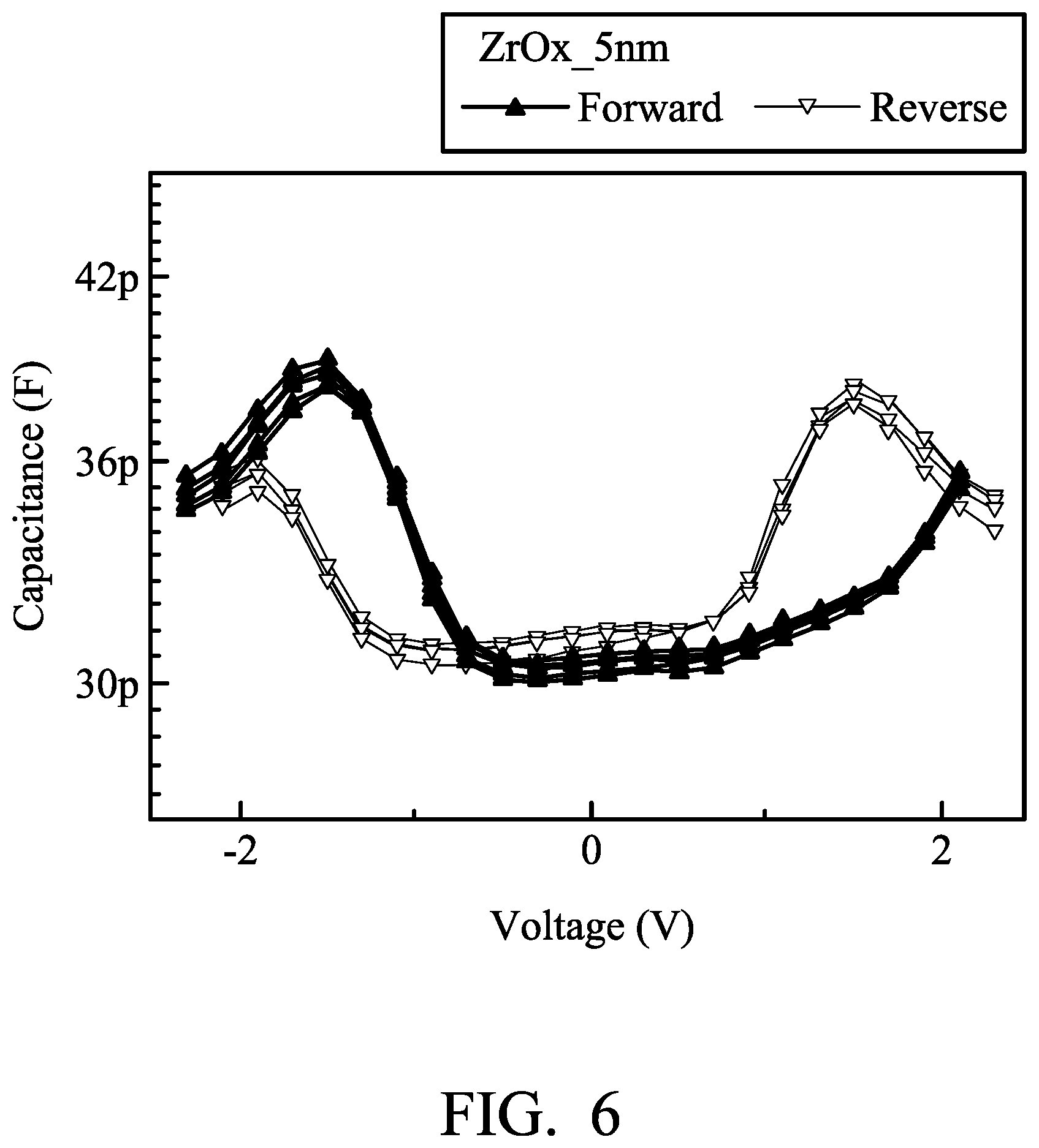
FIG. 6 is a capacitance-voltage characteristic diagram of an antiferroelectric layer in accordance with one embodiment of the disclosure;
FIG. 7 is a capacitance-voltage characteristic diagram of a ferroelectric layer in accordance with one embodiment of the disclosure; and
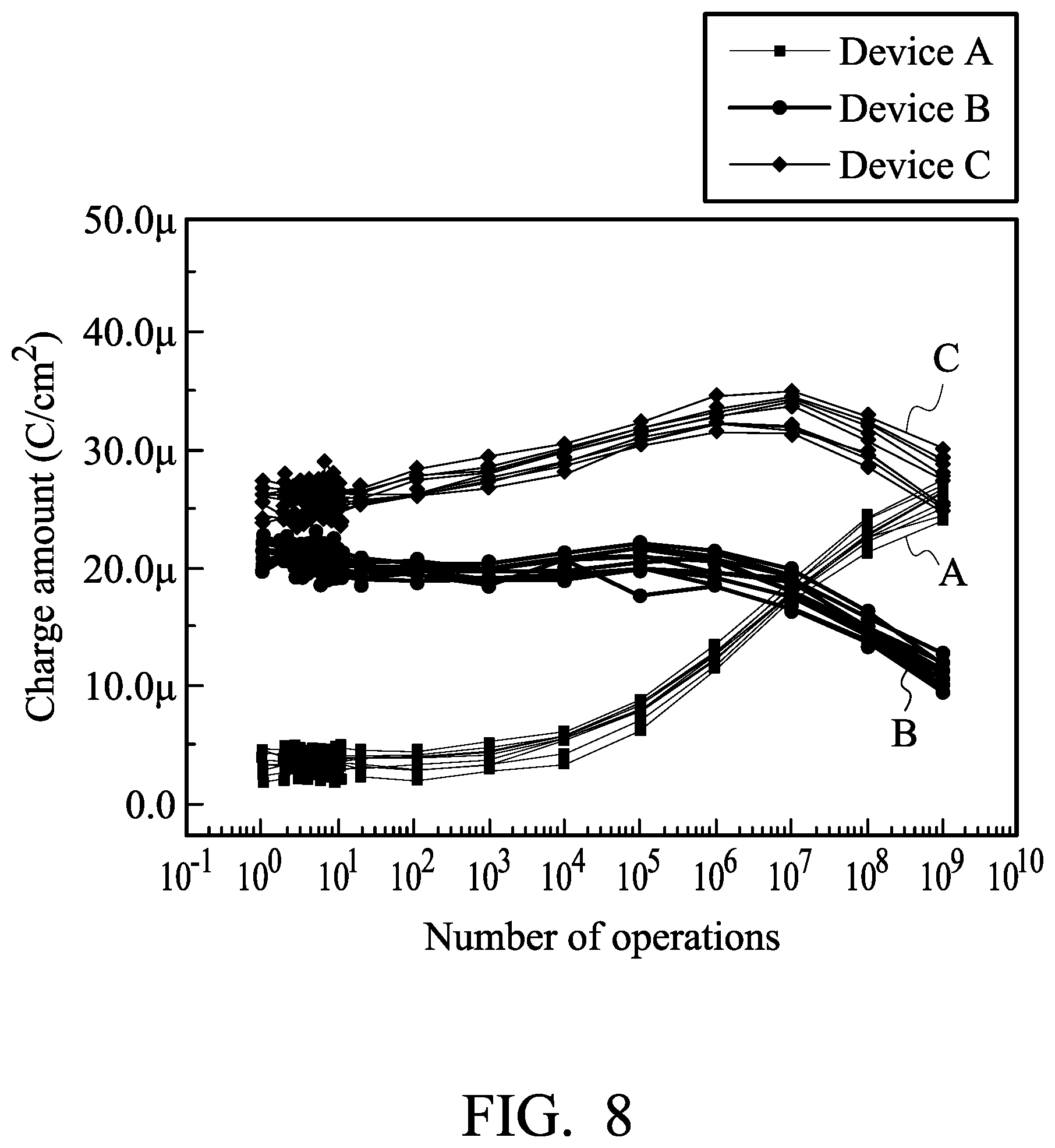
FIG. 8 shows a relationship between the charge amount and the number of operations of a ferroelectric memory in accordance with one embodiment of the disclosure.
DETAILED DESCRIPTION
The following description is of the best-contemplated mode of carrying out the disclosure. This description is made for the purpose of illustrating the general principles of the disclosure and should not be taken in a limiting sense. The scope of the disclosure is determined by reference to the appended claims.
In order to increase the number of operations of ferroelectric memories, the disclosure provides a ferroelectric memory. An antiferroelectric (AFE) layer with ferroelectric-delayed wake-up property is combined with a ferroelectric (FE) layer and applied to the ferroelectric memory, wherein the antiferroelectric (AFE) layer is in contact with the ferroelectric (FE) layer.
Referring to FIG. 1, in accordance with one embodiment of the disclosure, a ferroelectric memory 10 is provided. FIG. 1 is a cross-sectional view of the ferroelectric memory 10.
The ferroelectric memory (ferroelectric RAM) 10 includes a first electrode 12, a second electrode 14, a ferroelectric layer 16, and an antiferroelectric layer 18. The first electrode 12 is opposite to the second electrode 14. The ferroelectric layer 16 is disposed between the first electrode 12 and the second electrode 14. The antiferroelectric layer 18 is disposed between the first electrode 12 and the ferroelectric layer 16. The antiferroelectric layer 18 is in contact with the ferroelectric layer 16.
In some embodiments, the first electrode 12 and the second electrode 14 may include, for example, semiconductor, conductive dielectric or metal. In one embodiment, the first electrode 12 and the second electrode 14 may include the following materials, but not limited thereto, for example, zirconium (Zr), hafnium (Hf), titanium oxide (TiO.sub.x), titanium nitride (TiN), titanium (Ti), titanium oxynitride (TiON), tantalum (Ta), tantalum nitride (TaN), tantalum silicide (TaSi), tantalum carbonitride (TaCN), titanium aluminum nitride (TiAlN), zinc (Zn), zinc oxide (ZnO), nickel (Ni), nickel silicide (NiSi), carbon (C), silicon (Si), silicon oxide (SiO.sub.x), silicon nitride (SiN.sub.x), silicon oxynitride (SiON.sub.x), germanium (Ge), platinum (Pt), aluminum (Al), aluminum nitride (AlN), yttrium (Y), gadolinium (Gd), strontium (Sr), tungsten (W), tungsten silicide (WSi), tungsten nitride (WN), gallium (Ga), or gallium nitride (GaN).
In one embodiment, the ferroelectric layer 16 may include the following materials, but not limited thereto, for example, hafnium zirconium oxide (HfZrO.sub.x), hafnium silicon oxide (HfSiO.sub.x), hafnium oxide (HfO.sub.x), hafnium yttrium oxide (HfYO.sub.x), hafnium gadolinium oxide (HfGdO.sub.x), hafnium strontium oxide (HfSrO.sub.x), strontium titanium oxide (SrTiO.sub.x), strontium calcium titanate (SrCaTiO.sub.3), Ag(Nb.sub.1-xTa.sub.x)O.sub.3, barium strontium titanate (BaSrTiO.sub.3), or barium titanate (BaTiO.sub.3).
In this embodiment, the ferroelectric layer 16 is hafnium zirconium oxide (HfZrO.sub.x). In hafnium zirconium oxide (HfZrO.sub.x), the content of hafnium is higher than that of zirconium.
In one embodiment, the antiferroelectric layer 18 may include the following materials, but not limited thereto, for example, hafnium zirconium oxide (HfZrO.sub.x), zirconium oxide (ZrO.sub.x), hafnium silicon oxide (HfSiO.sub.x), hafnium aluminum oxide (HfAlO.sub.x), strontium titanium oxide (SrTiO.sub.x), strontium calcium titanate (SrCaTiO.sub.3), Ag(Nb.sub.1-xTa.sub.x)O.sub.3, barium strontium titanate (BaSrTiO.sub.3), or barium titanate (BaTiO.sub.3).
In this embodiment, the antiferroelectric layer 18 is hafnium zirconium oxide (HfZrO.sub.x). In hafnium zirconium oxide (HfZrO.sub.x), the content of zirconium is higher than that of hafnium.
In one embodiment, the compositions of the ferroelectric layer 16 and the antiferroelectric layer 18 may be similar materials to avoid creating an interface between the two layers. In some embodiments, the thickness of the ferroelectric layer 16 may be the same as or different from that of the antiferroelectric layer 18. In some embodiments, the total thickness "T" of the ferroelectric layer 16 and the antiferroelectric layer 18 is in a range from about 5 nm to about 15 nm.
Referring to FIG. 2, in accordance with one embodiment of the disclosure, a ferroelectric memory 100 is provided. FIG. 2 is a cross-sectional view of the ferroelectric memory 100.
The ferroelectric memory (ferroelectric RAM) 100 includes a first electrode 120, a second electrode 140, a ferroelectric layer 160, a first antiferroelectric layer 180, and a second antiferroelectric layer 190. The first electrode 120 is opposite to the second electrode 140. The ferroelectric layer 160 is disposed between the first electrode 120 and the second electrode 140. The first antiferroelectric layer 180 is disposed between the first electrode 120 and the ferroelectric layer 160. The second antiferroelectric layer 190 is disposed between the second electrode 140 and the ferroelectric layer 160. The first antiferroelectric layer 180 and the second antiferroelectric layer 190 are in contact with the ferroelectric layer 160.
In one embodiment, the first electrode 120 and the second electrode 140 may include, for example, semiconductor, conductive dielectric or metal. In some embodiments, the first electrode 120 and the second electrode 140 may include the following materials, but not limited thereto, for example, zirconium (Zr), hafnium (Hf), titanium oxide (TiO.sub.x), titanium nitride (TiN), titanium (Ti), titanium oxynitride (TiON), tantalum (Ta), tantalum nitride (TaN), tantalum silicide (TaSi), tantalum carbonitride (TaCN), titanium aluminum nitride (TiAlN), zinc (Zn), zinc oxide (ZnO), nickel (Ni), nickel silicide (NiSi), carbon (C), silicon (Si), silicon oxide (SiO.sub.x), silicon nitride (SiN.sub.x), silicon oxynitride (SiON.sub.x), germanium (Ge), platinum (Pt), aluminum (Al), aluminum nitride (AlN), yttrium (Y), gadolinium (Gd), strontium (Sr), tungsten (W), tungsten silicide (WSi), tungsten nitride (WN), gallium (Ga), or gallium nitride (GaN).
In one embodiment, the ferroelectric layer 160 may include the following materials, but not limited thereto, for example, hafnium zirconium oxide (HfZrO.sub.x), hafnium silicon oxide (HfSiO.sub.x), hafnium oxide (HfO.sub.x), hafnium yttrium oxide (HfYO.sub.x), hafnium gadolinium oxide (HfGdO.sub.x), hafnium strontium oxide (HfSrO.sub.x), strontium titanium oxide (SrTiO.sub.x), strontium calcium titanate (SrCaTiO.sub.3), Ag(Nb.sub.1-xTa.sub.x)O.sub.3, barium strontium titanate (BaSrTiO.sub.3), or barium titanate (BaTiO.sub.3).
In this embodiment, the ferroelectric layer 160 is hafnium zirconium oxide (HfZrO.sub.x). In hafnium zirconium oxide (HfZrO.sub.x), the content of hafnium is higher than that of zirconium.
In one embodiment, the first antiferroelectric layer 180 and the second antiferroelectric layer 190 may include the following materials, but not limited thereto, for example, hafnium zirconium oxide (HfZrO.sub.x), zirconium oxide (ZrO.sub.x), hafnium silicon oxide (HfSiO.sub.x), hafnium aluminum oxide (HfAlO.sub.x), strontium titanium oxide (SrTiO.sub.x), strontium calcium titanate (SrCaTiO.sub.3), Ag(Nb.sub.1-xTa.sub.x)O.sub.3, barium strontium titanate (BaSrTiO.sub.3), or barium titanate (BaTiO.sub.3).
In this embodiment, the first antiferroelectric layer 180 and the second antiferroelectric layer 190 are hafnium zirconium oxide (HfZrO.sub.x). In hafnium zirconium oxide (HfZrO.sub.x), the content of zirconium is higher than that of hafnium.
In one embodiment, the compositions of the ferroelectric layer 160, the first antiferroelectric layer 180 and the second antiferroelectric layer 190 may be similar materials to avoid creating interfaces between the layers. In some embodiments, the thickness of the ferroelectric layer 160, the first antiferroelectric layer 180 and the second antiferroelectric layer 190 may be the same or different therebetween. In some embodiments, the total thickness "T" of the ferroelectric layer 160, the first antiferroelectric layer 180 and the second antiferroelectric layer 190 is in a range from about 5 nm to about 15 nm.
Referring to FIG. 3, in accordance with one embodiment of the disclosure, a ferroelectric memory 200 is provided. FIG. 3 is a cross-sectional view of the ferroelectric memory 200.
The ferroelectric memory (ferroelectric RAM) 200 includes a first electrode 220, a second electrode 240, a plurality of ferroelectric layers 260, and a plurality of antiferroelectric layers 280. The first electrode 220 is opposite to the second electrode 240. The ferroelectric layers 160 and the antiferroelectric layers 280 are disposed between the first electrode 220 and the second electrode 240 and alternately arranged in a horizontal direction 290. The antiferroelectric layers 280 are in contact with the ferroelectric layers 260, for example, the both sides (280a and 280b) of the antiferroelectric layers 280 are in contact with the adjacent ferroelectric layers 260.
In one embodiment, the first electrode 220 and the second electrode 240 may include, for example, semiconductor, conductive dielectric or metal. In some embodiments, the first electrode 220 and the second electrode 240 may include the following materials, but not limited thereto, for example, zirconium (Zr), hafnium (Hf), titanium oxide (TiO.sub.x), titanium nitride (TiN), titanium (Ti), titanium oxynitride (TiON), tantalum (Ta), tantalum nitride (TaN), tantalum silicide (TaSi), tantalum carbonitride (TaCN), titanium aluminum nitride (TiAlN), zinc (Zn), zinc oxide (ZnO), nickel (Ni), nickel silicide (NiSi), carbon (C), silicon (Si), silicon oxide (SiO.sub.x), silicon nitride (SiN.sub.x), silicon oxynitride (SiON.sub.x), germanium (Ge), platinum (Pt), aluminum (Al), aluminum nitride (AlN), yttrium (Y), gadolinium (Gd), strontium (Sr), tungsten (W), tungsten silicide (WSi), tungsten nitride (WN), gallium (Ga), or gallium nitride (GaN).
In one embodiment, the ferroelectric layers 260 may include the following materials, but not limited thereto, for example, hafnium zirconium oxide (HfZrO.sub.x), hafnium silicon oxide (HfSiO.sub.x), hafnium oxide (HfO.sub.x), hafnium yttrium oxide (HfYO.sub.x), hafnium gadolinium oxide (HfGdO.sub.x), hafnium strontium oxide (HfSrO.sub.x), strontium titanium oxide (SrTiO.sub.x), strontium calcium titanate (SrCaTiO.sub.3), Ag(Nb.sub.1-xTa.sub.x)O.sub.3, barium strontium titanate (BaSrTiO.sub.3), or barium titanate (BaTiO.sub.3).
In this embodiment, the ferroelectric layers 260 are hafnium zirconium oxide (HfZrO.sub.x). In hafnium zirconium oxide (HfZrO.sub.x), the content of hafnium is higher than that of zirconium.
In one embodiment, the antiferroelectric layers 280 may include the following materials, but not limited thereto, for example, hafnium zirconium oxide (HfZrO.sub.x), zirconium oxide (ZrO.sub.x), hafnium silicon oxide (HfSiO.sub.x), hafnium aluminum oxide (HfAlO.sub.x), strontium titanium oxide (SrTiO.sub.x), strontium calcium titanate (SrCaTiO.sub.3), Ag(Nb.sub.1-xTa.sub.x)O.sub.3, barium strontium titanate (BaSrTiO.sub.3), or barium titanate (BaTiO.sub.3).
In this embodiment, the antiferroelectric layers 280 are hafnium zirconium oxide (HfZrO.sub.x). In hafnium zirconium oxide (HfZrO.sub.x), the content of zirconium is higher than that of hafnium.
In one embodiment, the compositions of the ferroelectric layers 260 and the antiferroelectric layers 280 may be similar materials to avoid creating interfaces between the layers. In one embodiment, the total thickness T' of the ferroelectric layer 260 and the antiferroelectric layer 280 is in a range from about 5 nm to about 15 nm.
Referring to FIG. 4, in accordance with one embodiment of the disclosure, a ferroelectric memory 500 is provided. FIG. 4 is a cross-sectional view of the ferroelectric memory 500.
The ferroelectric memory (ferroelectric RAM) 500 includes a first electrode 520, a second electrode 540, a ferroelectric layer 560, and an antiferroelectric layer 580. The first electrode 520 is opposite to the second electrode 540. The ferroelectric layer 560 is disposed between the first electrode 520 and the second electrode 540. The antiferroelectric layer 580 is disposed between the second electrode 540 and the ferroelectric layer 560. The antiferroelectric layer 580 is in contact with the ferroelectric layer 560.
In one embodiment, the first electrode 520 and the second electrode 540 may include, for example, semiconductor, conductive dielectric or metal. In some embodiments, the first electrode 520 and the second electrode 540 may include the following materials, but not limited thereto, for example, zirconium (Zr), hafnium (Hf), titanium oxide (TiO.sub.x), titanium nitride (TiN), titanium (Ti), titanium oxynitride (TiON), tantalum (Ta), tantalum nitride (TaN), tantalum silicide (TaSi), tantalum carbonitride (TaCN), titanium aluminum nitride (TiAlN), zinc (Zn), zinc oxide (ZnO), nickel (Ni), nickel silicide (NiSi), carbon (C), silicon (Si), silicon oxide (SiO.sub.x), silicon nitride (SiN.sub.x), silicon oxynitride (SiON.sub.x), germanium (Ge), platinum (Pt), aluminum (Al), aluminum nitride (AlN), yttrium (Y), gadolinium (Gd), strontium (Sr), tungsten (W), tungsten silicide (WSi), tungsten nitride (WN), gallium (Ga), or gallium nitride (GaN).
In one embodiment, the ferroelectric layer 560 may include the following materials, but not limited thereto, for example, hafnium zirconium oxide (HfZrO.sub.x), hafnium silicon oxide (HfSiO.sub.x), hafnium oxide (HfO.sub.x), hafnium yttrium oxide (HfYO.sub.x), hafnium gadolinium oxide (HfGdO.sub.x), hafnium strontium oxide (HfSrO.sub.x), strontium titanium oxide (SrTiO.sub.x), strontium calcium titanate (SrCaTiO.sub.3), Ag(Nb.sub.1-xTa.sub.x)O.sub.3, barium strontium titanate (BaSrTiO.sub.3), or barium titanate (BaTiO.sub.3).
In this embodiment, the ferroelectric layer 560 is hafnium zirconium oxide (HfZrO.sub.x). In hafnium zirconium oxide (HfZrO.sub.x), the content of hafnium is higher than that of zirconium.
In one embodiment, the antiferroelectric layer 580 may include the following materials, but not limited thereto, for example, hafnium zirconium oxide (HfZrO.sub.x), zirconium oxide (ZrO.sub.x), hafnium silicon oxide (HfSiO.sub.x), hafnium aluminum oxide (HfAlO.sub.x), strontium titanium oxide (SrTiO.sub.x), strontium calcium titanate (SrCaTiO.sub.3), Ag(Nb.sub.1-xTa.sub.x)O.sub.3, barium strontium titanate (BaSrTiO.sub.3), or barium titanate (BaTiO.sub.3).
In this embodiment, the antiferroelectric layer 580 is hafnium zirconium oxide (HfZrO.sub.x). In hafnium zirconium oxide (HfZrO.sub.x), the content of zirconium is higher than that of hafnium.
In one embodiment, the compositions of the ferroelectric layer 560 and the antiferroelectric layer 580 may be similar materials to avoid creating an interface between the two layers. In some embodiments, the thickness of the ferroelectric layer 560 may be the same as or different from that of the antiferroelectric layer 580. In some embodiments, the total thickness "T" of the ferroelectric layer 560 and the antiferroelectric layer 580 is in a range from about 5 nm to about 15 nm.
Referring to FIG. 5, in accordance with one embodiment of the disclosure, a ferroelectric memory 1000 is provided. FIG. 5 is a cross-sectional view of the ferroelectric memory 1000.
The ferroelectric memory (ferroelectric RAM) 1000 includes a first electrode 1200, a second electrode 1400, a first ferroelectric layer 1600, a second ferroelectric layer 1700, and an antiferroelectric layer 1800. The first electrode 1200 is opposite to the second electrode 1400. The antiferroelectric layer 1800 is disposed between the first electrode 1200 and the second electrode 1400. The first ferroelectric layer 1600 is disposed between the first electrode 1200 and the antiferroelectric layer 1800. The second ferroelectric layer 1700 is disposed between the second electrode 1400 and the antiferroelectric layer 1800. The first ferroelectric layer 1600 and the second ferroelectric layer 1700 are in contact with the antiferroelectric layer 1800.
In one embodiment, the first electrode 1200 and the second electrode 1400 may include, for example, semiconductor, conductive dielectric or metal. In one embodiment, the first electrode 1200 and the second electrode 1400 may include the following materials, but not limited thereto, for example, zirconium (Zr), hafnium (Hf), titanium oxide (TiO.sub.x), titanium nitride (TiN), titanium (Ti), titanium oxynitride (TiON), tantalum (Ta), tantalum nitride (TaN), tantalum silicide (TaSi), tantalum carbonitride (TaCN), titanium aluminum nitride (TiAlN), zinc (Zn), zinc oxide (ZnO), nickel (Ni), nickel silicide (NiSi), carbon (C), silicon (Si), silicon oxide (SiO.sub.x), silicon nitride (SiN.sub.x), silicon oxynitride (SiON.sub.x), germanium (Ge), platinum (Pt), aluminum (Al), aluminum nitride (AlN), yttrium (Y), gadolinium (Gd), strontium (Sr), tungsten (W), tungsten silicide (WSi), tungsten nitride (WN), gallium (Ga), or gallium nitride (GaN).
In one embodiment, the first ferroelectric layer 1600 and the second ferroelectric layer 1700 may include the following materials, but not limited thereto, for example, hafnium zirconium oxide (HfZrO.sub.x), hafnium silicon oxide (HfSiO.sub.x), hafnium oxide (HfO.sub.x), hafnium yttrium oxide (HfYO.sub.x), hafnium gadolinium oxide (HfGdO.sub.x), hafnium strontium oxide (HfSrO.sub.x), strontium titanium oxide (SrTiO.sub.x), strontium calcium titanate (SrCaTiO.sub.3), Ag(Nb.sub.1-xTa.sub.x)O.sub.3, barium strontium titanate (BaSrTiO.sub.3), or barium titanate (BaTiO.sub.3).
In this embodiment, the first ferroelectric layer 1600 and the second ferroelectric layer 1700 are hafnium zirconium oxide (HfZrO.sub.x). In hafnium zirconium oxide (HfZrO.sub.x), the content of hafnium is higher than that of zirconium.
In one embodiment, the antiferroelectric layer 1800 may include the following materials, but not limited thereto, for example, hafnium zirconium oxide (HfZrO.sub.x), zirconium oxide (ZrO.sub.x), hafnium silicon oxide (HfSiO.sub.x), hafnium aluminum oxide (HfAlO.sub.x), strontium titanium oxide (SrTiO.sub.x), strontium calcium titanate (SrCaTiO.sub.3), Ag(Nb.sub.1-xTa.sub.x)O.sub.3, barium strontium titanate (BaSrTiO.sub.3), or barium titanate (BaTiO.sub.3).
In this embodiment, the antiferroelectric layer 1800 is hafnium zirconium oxide (HfZrO.sub.x). In hafnium zirconium oxide (HfZrO.sub.x), the content of zirconium is higher than that of hafnium.
In one embodiment, the compositions of the first ferroelectric layer 1600, the second ferroelectric layer 1700 and the antiferroelectric layer 1800 may be similar materials to avoid creating interfaces between the layers. In one embodiment, the thickness of the first ferroelectric layer 1600, the second ferroelectric layer 1700 and the antiferroelectric layer 1800 may be the same or different therebetween. In some embodiments, the total thickness "T" of the first ferroelectric layer 1600, the second ferroelectric layer 1700 and the antiferroelectric layer 1800 is in a range from about 5 nm to about 15 nm.
EXAMPLES
Example 1
Measurement of the Capacitance-Voltage Characteristic of the Antiferroelectric (AFE) Layer
In this example, the capacitance-voltage characteristics of the zirconium oxide (ZrO) antiferroelectric (AFE) layer having a thickness of 5 nm was measured, and the measurement results are shown in FIG. 6. In FIG. 6, according to the curve of the capacitance value of the antiferroelectric layer with the applied voltage, the zirconium oxide (ZrO) component has antiferroelectric characteristics. In the process of applying voltage, the characteristic of the antiferroelectric layer is converted from the originally antiferroelectric characteristic into the ferroelectric characteristic so that the antiferroelectric layer has a ferroelectric-delayed wake-up characteristic. If the antiferroelectric layer with the ferroelectric-delayed wake-up characteristic is applied to the ferroelectric memory of the disclosure, the fatigue effect of the ferroelectric layer is effectively compensated.
Example 2
Measurement of the Capacitance-Voltage Characteristic of the Ferroelectric (FE) Layer
In this example, the capacitance-voltage characteristics of the zirconium oxide (HfZrO) ferroelectric (FE) layer having a thickness of 10 nm was measured, and the measurement results are shown in FIG. 7. In FIG. 7, according to the curve of the capacitance value of the ferroelectric layer with the applied voltage, the zirconium oxide (HfZrO) component has ferroelectric characteristics. In the process of applying voltage, the ferroelectric layer gradually produced the fatigue effect, resulting in decrease of the polarization thereof. If the ferroelectric layer is combined with the antiferroelectric layer with the ferroelectric-delayed wake-up characteristic of Example 1 and applied to the ferroelectric memory of the disclosure, the fatigue effect produced by the ferroelectric layer is effectively compensated.
Example 3
The Relationship Between the Charge Amount and the Number of Operations of the Ferroelectric Memory
In this example, the variation in charge amount of three ferroelectric memories (Devices A, B and C) under different numbers of operations was measured. Device A was an antiferroelectric device composed of a 5 nm-thick zirconium oxide (HfZrO) antiferroelectric layer. Device B was a ferroelectric device composed of a 10 nm-thick zirconium oxide (HfZrO) ferroelectric layer. Device C was an integrated device composed of a 5 nm-thick zirconium oxide (HfZrO) antiferroelectric layer and a 5 nm-thick zirconium oxide (HfZrO) ferroelectric layer. In Device A, the variation in charge amount thereof was measured under the strength of the electric field of 2.8 MV/cm and the operating frequency of 5 M-Hz. In Device B, the variation in charge amount thereof was measured under the strength of the electric field of 2.0 MV/cm and the operating frequency of 5 M-Hz. In Device C, the variation in charge amount thereof was measured under the strength of the electric field of 2.4 MV/cm and the operating frequency of 5 M-Hz. The measurement results (curves A, B and C) of Devices A, B and C are shown in FIG. 8.
In FIG. 8, according to the curve of the charge amount of each device with the number of operations, the charge amount of Device A (the curve A) increased as the number of operations increased, which means that Device A had ferroelectric-delayed wake-up characteristic. The charge amount of Device B (the curve B) began to decrease as the number of operations was increased to a specific value (for example, after the number of operations reached 10.sup.5), which means that Device B produced the fatigue effect after the number of operations reached 10.sup.5. The charge amount of Device C (the curve C) was increased first and then decreased as the number of operations increased, which means that although the ferroelectric layer disposed in Device C produced the fatigue effect, the antiferroelectric layer disposed in Device C simultaneously induced the ferroelectric-delayed wake-up characteristic, and this phenomenon effectively compensated for the fatigue effect generated by the ferroelectric layer. Therefore, it can be seen from the curve C that the charge amount of Device C gradually decreased after the number of operations reached 10.sup.7 (>10.sup.5). Device C can effectively increase the number of operations thereof compared to Device B.
The disclosure applies an antiferroelectric (AFE) layer with a ferroelectric-delayed wake-up property and a ferroelectric (FE) layer to the ferroelectric memory, and the antiferroelectric (AFE) layer is in contact with the ferroelectric (FE) layer. Although the ferroelectric layer generates a fatigue effect during the operation of the component, the property of the antiferroelectric layer in the component is converted from the originally antiferroelectric property to the ferroelectric property, and thus the ferroelectric-delayed wake-up property is provided. This phenomenon can just compensate for the fatigue effect generated by the ferroelectric layer, thereby effectively improving the number of operations of the component by 10.sup.10 or more, and slowing down the operation deterioration.
While the disclosure has been described by way of example and in terms of embodiment, it is to be understood that the disclosure is not limited thereto. On the contrary, it is intended to cover various modifications and similar arrangements (as would be apparent to those skilled in the art). Therefore, the scope of the appended claims should be accorded the broadest interpretation so as to encompass all such modifications and similar arrangements.
* * * * *
D00000
D00001
D00002
D00003
D00004
D00005
D00006
XML
uspto.report is an independent third-party trademark research tool that is not affiliated, endorsed, or sponsored by the United States Patent and Trademark Office (USPTO) or any other governmental organization. The information provided by uspto.report is based on publicly available data at the time of writing and is intended for informational purposes only.
While we strive to provide accurate and up-to-date information, we do not guarantee the accuracy, completeness, reliability, or suitability of the information displayed on this site. The use of this site is at your own risk. Any reliance you place on such information is therefore strictly at your own risk.
All official trademark data, including owner information, should be verified by visiting the official USPTO website at www.uspto.gov. This site is not intended to replace professional legal advice and should not be used as a substitute for consulting with a legal professional who is knowledgeable about trademark law.