Wide band receiver front end for rotational spectroscopy
Zhong , et al. A
U.S. patent number 10,749,559 [Application Number 15/628,363] was granted by the patent office on 2020-08-18 for wide band receiver front end for rotational spectroscopy. This patent grant is currently assigned to Board of Regents, The University of Texas System. The grantee listed for this patent is Board of Regents, University of Texas. Invention is credited to Wooyeol Choi, Kenneth K. O, Qian Zhong.

| United States Patent | 10,749,559 |
| Zhong , et al. | August 18, 2020 |
Wide band receiver front end for rotational spectroscopy
Abstract
A receiver receives a wide band signal in a range comprising a front end to the receiver including a complementary metal-oxide-semiconductor (CMOS). The CMOS includes a dipole antenna that receives a received signal; a hybrid-based broadband isolation structure that receives the received signal and a local oscillator LO signal and passes through the LO signal to a sub-harmonic mixer. The sub-harmonic mixer mixes the received signal with the local oscillator signal to generate an intermediate frequency (IF) signal to the hybrid-based broadband isolation structure.
| Inventors: | Zhong; Qian (Dallas, TX), O; Kenneth K. (Plano, TX), Choi; Wooyeol (Richardson, TX) | ||||||||||
|---|---|---|---|---|---|---|---|---|---|---|---|
| Applicant: |
|
||||||||||
| Assignee: | Board of Regents, The University of
Texas System (Austin, TX) |
||||||||||
| Family ID: | 60660441 | ||||||||||
| Appl. No.: | 15/628,363 | ||||||||||
| Filed: | June 20, 2017 |
Prior Publication Data
| Document Identifier | Publication Date | |
|---|---|---|
| US 20170366214 A1 | Dec 21, 2017 | |
Related U.S. Patent Documents
| Application Number | Filing Date | Patent Number | Issue Date | ||
|---|---|---|---|---|---|
| 62352117 | Jun 20, 2016 | ||||
| Current U.S. Class: | 1/1 |
| Current CPC Class: | H04B 1/40 (20130101); H04B 1/3827 (20130101); G01J 3/42 (20130101); G01J 3/00 (20130101) |
| Current International Class: | H04B 1/3827 (20150101); H04B 1/40 (20150101); G01J 3/00 (20060101); G01J 3/42 (20060101) |
References Cited [Referenced By]
U.S. Patent Documents
| 7376403 | May 2008 | Wanke |
| 7420225 | September 2008 | Wanke |
| 8748822 | June 2014 | Gerecht |
| 2012/0181431 | July 2012 | Mitin |
| 2016/0131600 | May 2016 | Pate |
Other References
|
E Ojefors, et al., "Active 220- and 325-GHz Frequency Multiplier Chains in an SiGe HBT Technology," IEEE Transactions on Microwave Theory and Techniques, May 2011, pp. 1311-1318, vol. 59, No. 5. cited by applicant . H. Lin, G. Rebeiz, "A 200-245 GHz Balanced Frequency Doubler with Peak Output Power of +2 dBm," CSICS, Oct. 2013, pp. 1-4, San Diego, CA. cited by applicant . K. Schmalz, et al., "245 GHz SiGe Transmitter with Integrated Antenna and External PLL," Microwave Symposium Digest, Jun. 2013, pp. 1-3. cited by applicant . Medvedev, et al., "Submillimeter spectroscopy for chemical analysis with absolute specificity," Optics Letters, May 2010, pp. 1533-1535, vol. 35, No. 10. cited by applicant . N. Sarmah, et al, "235-275 GHz (x16) Frequency Multiplier Chains with up to 0 dBm Peak Output Power and Low DC Power Consumption," Radio Frequency Integrated Circuits Symposium, 2014, pp. 181-184. cited by applicant . N. Sharma, et al., "160-310 GHz Frequency Doubler in 65-nm CMOS with 3-dBm Peak Output Power for Rotational Spectroscopy," Radio Frequency Integrated Circuts Symposium, Jul. 2016, pp. 186-189. cited by applicant . N. Sharma, et al., "85-to-127 GHz CMOS Transmitter for Rotational Spectroscopy," Custom Integrated Circuits Conference, 2014, pp. 298-301. cited by applicant . O. Momeni, E. Afshari, "A Broadband mm-Wave and Terahertz Traveling-Wave Frequency Multiplieron CMOS," IEEE Journal of Solid-State Circuits, Dec. 2011, pp. 2966-2976, vol. 46, No. 12. cited by applicant . W. Chan, J. Long, "A 60-GHz Band 2 2 Phased-Array Transmitter in 65-nm CMOS," IEEE Journal of Solid-State Circuits, Dec. 2010, pp. 2682-2695, vol. 45, No. 12. cited by applicant . Z. Wang, et al., "A CMOS 210-GHz Fundamental Transceiver With OOK Modulation," IEEE Journal of Solid-State Circuits, Mar. 2014, pp. 564-580, vol. 49, No. 3. cited by applicant. |
Primary Examiner: Taningco; Marcus H
Attorney, Agent or Firm: Schott, PC.
Claims
The invention claimed is:
1. A receiver for receiving a wide band signal in a range comprising a front end to the receiver comprising a complementary metal-oxide-semiconductor (CMOS) comprising: a dipole antenna that receives a received signal; a hybrid-based broadband isolation structure that receives the received signal and a local oscillator LO signal and passes through the LO signal to a sub-harmonic mixer; and the sub-harmonic mixer that mixes the received signal with the local oscillator signal to generate an intermediate frequency (IF) signal to the hybrid-based broadband isolation structure.
2. The receiver of claim 1, wherein the dipole antenna's phase interference has a near constant phase shift over a frequency range from 200 to 300 GHz.
3. The receiver of claim 1, wherein the dipole antenna is mounted on a thickness of silicon, which is mounted on a reflector.
4. The receiver of claim 3, wherein the reflector comprises spaced-apart reflector portions mounted on a reflector surface.
5. The receiver of claim 4, wherein the spaced apart reflector portions are 30 .mu.m square and spaced apart at 10 .mu.m intervals.
6. The receiver of claim 3, wherein the thickness of silicon has a thickness dependent on m/2*.lamda., where m is an any integer, and .lamda. is a wavelength of an incident wave.
7. The receiver of claim 1, wherein the sub-harmonic mixer comprises an anti-parallel diode pair (APDP).
8. The receiver of claim 7, wherein the APDP comprises diode-connected transistors, wherein at least one of the diode connected transistors is connected directly through a ground.
9. The receiver of claim 8, wherein the APDP comprises diode-connected transistors, wherein another of the at least one of the diode connected transistors is connected to a ground through a resistor.
10. The receiver of claim 9, wherein the resistor is a 5 k.OMEGA. resistor.
11. The receiver of claim 1, wherein the hybrid-based broadband isolation structure provides port isolation and impedance matching over a 200-300 GHz frequency range.
12. The receiver of claim 1, wherein the hybrid-based broadband isolation structure comprises a grounded coplanar waveguide (GCPW), three-line transmission line (Tri-TL), and differential line, wherein the dipole antenna is connected to each of two of the transmission lines and the sub-harmonic mixer is connected to all of the transmission lines.
13. The receiver of claim 12, wherein the grounded coplanar waveguide is fed by an LO signal.
14. The receiver of claim 13, wherein the LO signal is delivered in even mode.
15. The receiver of claim 14, wherein the differential line is fed by the emitted signal.
16. The receiver of claim 15, wherein the emitted signal and the LO signal are isolated from one another.
17. The receiver of claim 16, wherein the emitted signal and LO signal are isolated from one another using two capacitors inserted into a ground path of the GCPW, wherein the capacitors serve as a short for emitted and LO signals.
18. The receiver of claim 17, wherein the IF signal is sent to a low noise amplifier, which amplifies the IF signal and sends the amplified IF signal to an IF detector, and then to a baseband output.
19. A rotational spectrometer for identifying gas molecules comprising: a transmitter that radiates electromagnetic waves into an absorption cell containing gas molecules, wherein the electromagnetic waves change a rotational state of the gas molecules and absorb some of the wave power that can be seen as a drop in power; and front end receiver the detects the drop in power as a wide band signal, the front end to the receiver comprising a complementary metal-oxide-semiconductor (CMOS) comprising: a dipole antenna that receives the wide band signal as a received signal; a hybrid-based broadband isolation structure that receives the received signal and a local oscillator LO signal and passes through the LO signal to a sub-harmonic mixer; and the sub-harmonic mixer that mixes the received signal with the local oscillator signal to generate an intermediate frequency (IF) signal to the hybrid-based broadband isolation structure. wherein the IF signal is sent to a low noise amplifier that amplifies the IF signal and sends the amplified IF signal to an IF detector, and then to a baseband output, wherein the baseband out signal that can be analyzed by a controlling computer to correspond the baseband output to a known drop in power corresponding to a specific gas.
20. The rotational spectrometer of claim 19, wherein the rotational spectrometer can be used to detect signals and identify gas molecules over a frequency range from 200 to 300 GHz.
Description
BACKGROUND
Portable gas spectroscopy may useful in settings that include indoor or confined space air monitoring and breath analysis. Current technologies include either small devices that detect a limited number of gas types (such as for common roadside alcohol breathalyzer tests) or may lack sensitivity. Larger devices may be able to scan for a broader number of gas types, but their size and power consumption may make them undesirable in many environments.
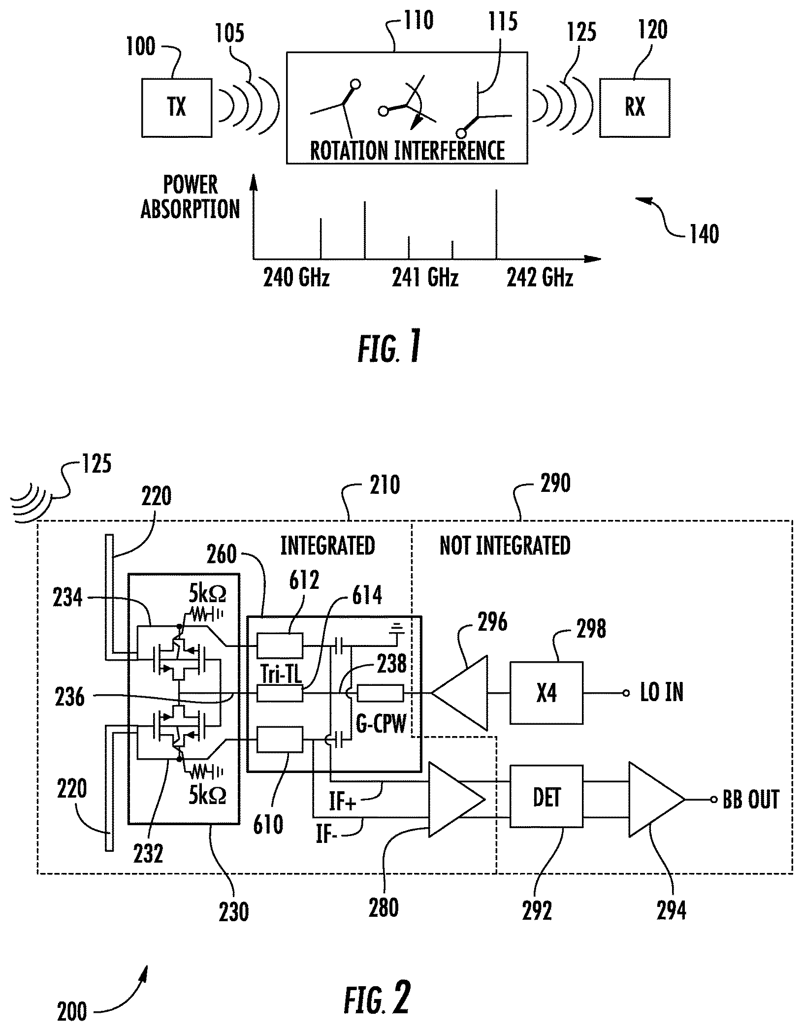
As an overview of the technology, electro-magnetic waves in the millimeter and submillimeter wave frequency ranges can be used for fast scan rotational spectroscopy to detect gas molecules and measure their concentrations. FIG. 1 shows the principle behind rotational spectroscopy, in which a transmitter 100 such as a VDI transmitter radiates electromagnetic waves 105 within a certain frequency range into an absorption cell 110 containing gas molecules 115. The waves change the rotational state of gas molecules and a part of the wave power is lost in this interaction. These results in a drop of power picked up 125 at a receiver (RX) 120 such as a VDI receiver or a spike. By sweeping the transmitter (TX) 100 output frequency, a sweep controlled by a computer (not shown), the receiver 120 may measure the frequency response of the absorption cell 110. As shown in the frequency vs power absorption graph 140, looking at the frequencies at which the waves are absorbed and the depth of absorption line, the presence of a particular molecule and its concentration may be determined.
Rotational spectrometers use a frequency multiplier chain driven from a signal generated using a synthesizer to generate the transmitter signal, and a diode based sub-harmonic mixer followed by an amplifier and a diode amplitude detector to measure the received signal amplitude. The frequency multiplier chain, mixer and diode may be fabricated using compound-semiconductor technologies. Rotational spectroscopy at 240-250 GHz has been demonstrated using SiGe heterojunction bipolar transistor (HBT) based radio frequency (RF) front-ends for transmission and reception and a spectrometer that measures 200-300 GHz frequency waves uses III-V technology (obtained by combining group III elements (Al, Ga, In) with group V elements (N, P, As, Sb)) but is both expensive and bulky.
SUMMARY OF THE EMBODIMENTS
A receiver receives a wide band signal in a range comprising a front end to the receiver including a complementary metal-oxide-semiconductor (CMOS). The CMOS includes a dipole antenna that receives a received signal; a hybrid-based broadband isolation structure that receives the received signal and a local oscillator LO signal and passes through the LO signal to a sub-harmonic mixer. The sub-harmonic mixer mixes the received signal with the local oscillator signal to generate an intermediate frequency (IF) signal to the hybrid-based broadband isolation structure.
BRIEF DESCRIPTION OF THE DRAWINGS
FIG. 1 shows a graphical overview of rotational spectroscopy.
FIG. 2 shows a schematic for a front-end for rotational spectroscopy that includes a sub-harmonic mixer, an on-chip antenna and an intermediate frequency amplifier.
FIG. 3 shows detection comparisons between 3 antenna designs.
FIG. 4 shows a comparison between the metal reflector and phase-compensated AMC reflector.
FIGS. 5A-5D show schematic diagrams of the mixer.
FIG. 6 is a schematic depiction of the hybrid structure.
DETAILED DESCRIPTION OF THE EMBODIMENTS
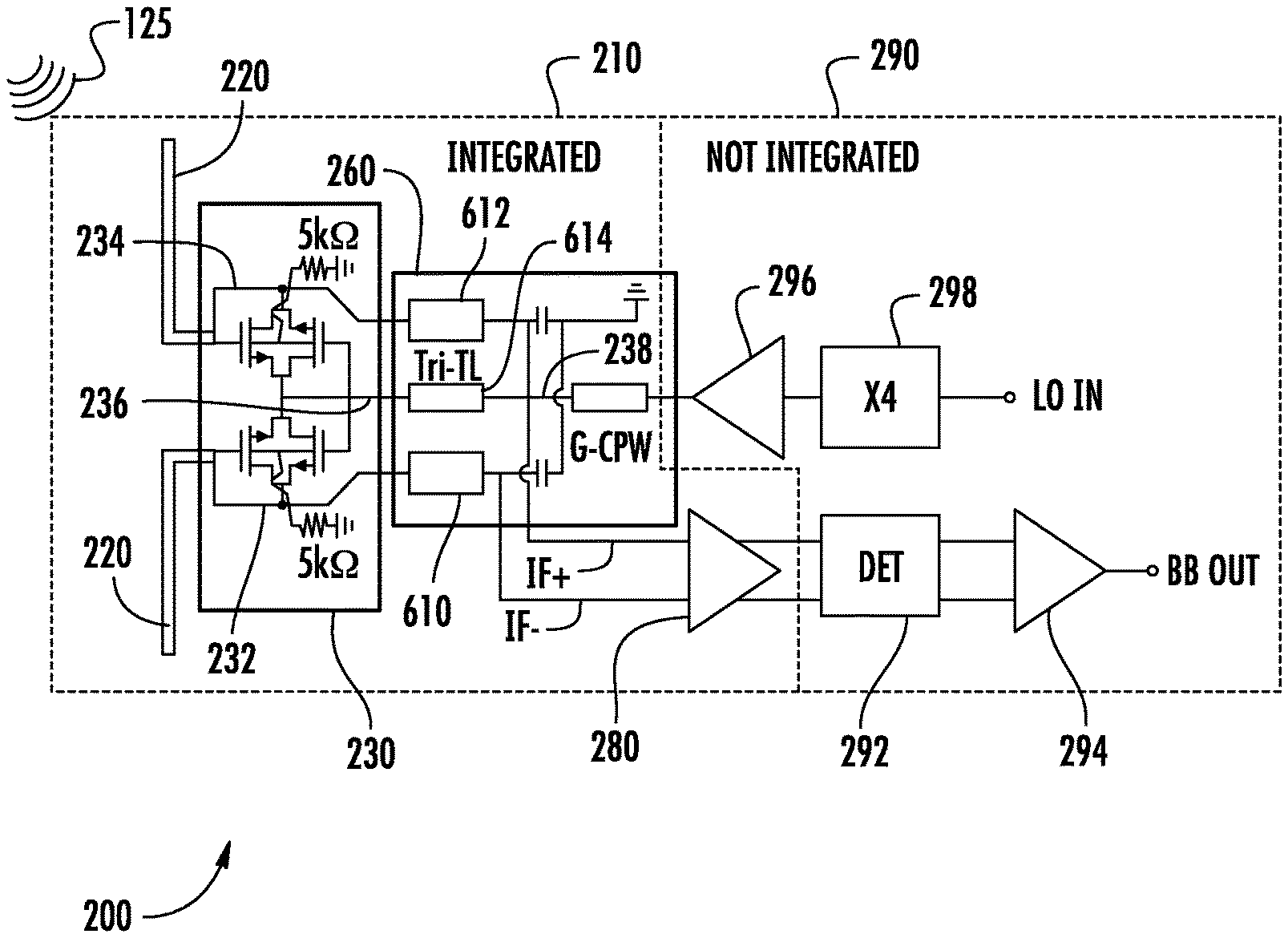
FIG. 2 shows a front-end receiver architecture 200 for rotational spectroscopy that includes an integrated system 210 and a non-integrated system 290. The integrated system 210 may use a complementary metal-oxide-semiconductor (CMOS) to conserve power and space and includes an on-chip dipole antenna 220, a sub-harmonic mixer 230 with a hybrid-based broadband isolation structure 260, and an intermediate frequency (IF) low noise amplifier 280.
The non-integrated system 290 may include an IF AM detector 292 connected to the IF low noise amplifier 280 and detector 292, which is itself connected to the baseband output 294. The local oscillator (LO) amplifier 296 that includes a frequency multiplier 298 connected to an LO input. Within this LO chain, the multiplier 298 takes input may receive input signals at 27-34 GHz and generates output signals at 110-145 GHz, although other frequencies are possible.
The LO driver may include two stages of neutralized differential common source stages to drive the LO port of the receiver front end 200 that requires 0-2 dBm power.
The receiver front end 200 and the integrated circuit 210 will be explained in more detail below, but in summary, the dipole antenna 220 detects a frequency of the emitted signal 125 to identify a power drop that corresponds to a certain gas in the absorption cell 110. It does this by processing, in the hybrid core 260, an amplified LO signal from the LO amplifier 296 and the emitted signal 125 received through the dipole antenna 220 processed through the subharmonic mixer 230, to generate to an IF signal to an IF amplifier 280, which in turn sends the IF amplified signal to a detector 292 that generates a detected output signal to a baseband output 294 to generate a baseband signal that can be analyzed by a controlling computer to determine the presence of a specific gas.
Dipole Antenna
Silicon on-chip antennas suffer from low gain and efficiency because of EM wave propagation into the silicon substrate. A way to mitigate this is to place a metal reflector at the backside of the chip to reflect the wave back into the air. By making the silicon thickness an odd multiple of one quarter wavelength (k/4), the reflected wave can be combined in-phase with the broadside radiation, improving the peak antenna gain.
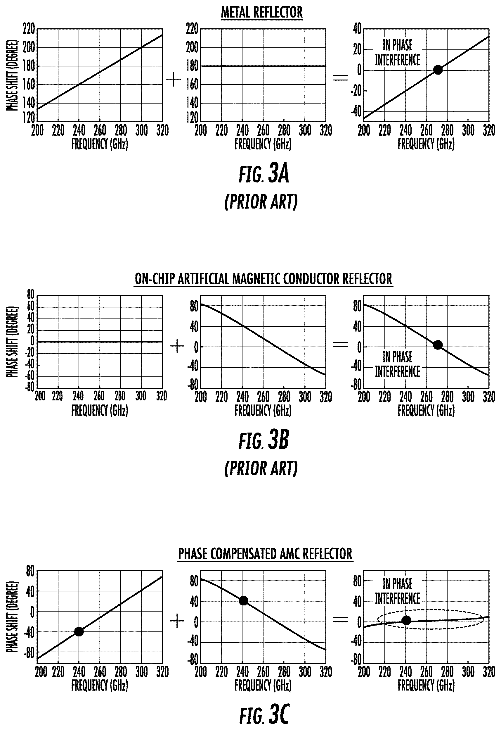
FIG. 3 shows detection comparisons between 3 antenna designs: (1) using a metal reflector assembly, (2) using an artificial magnetic conductor (AMC) reflector, and (3) using a phase-compensated AMC reflector. The three graphs for each assembly from left to right show the frequency vs phase shift measurements and their combined measurement for multiple phase shifts/frequencies. As can be seen for the metal reflector and AMC combined graph, the in-phase interference (the right-most graph varies with frequency, making them accurate only for a limited frequency. In contrast, the in-phase interference for a phase compensated AMC reflector has a near constant phase shift over a large frequency range, which makes it effective for use in a range from approximately 200-320 GHz.
Said another way, in the phase-compensated AMC construction, frequency responses of the phase shift due to the AMC and propagation through the substrate have opposite frequency dependences. When compensated, the phase shift can be kept less than +/-8.degree. and makes the antenna efficiency to be within 0.5 dB of the peak efficiency between 200 to 300 GHz.
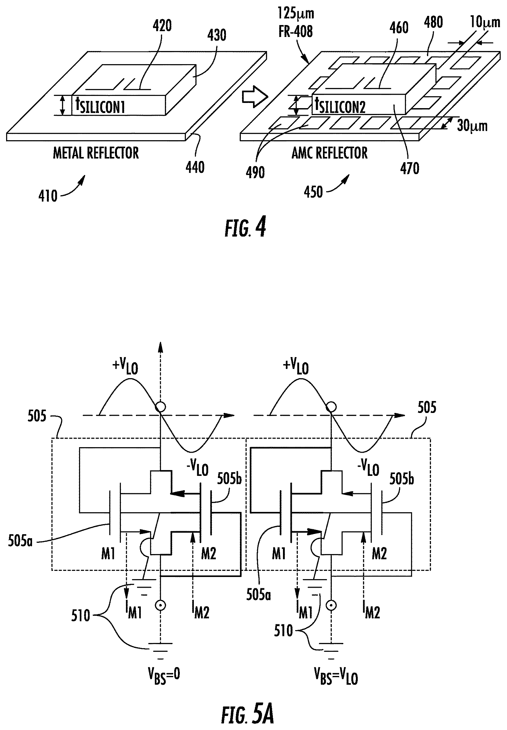
FIG. 4 shows a comparison between the metal reflector 410 and phase-compensated AMC reflector 450. In the traditional metal reflector, an antenna 420 is mounted on a thickness of silicon 430 on top of the reflector 440. In the traditional construction, the silicon thickness is dependent on k/4*.lamda., where k is an odd integer and .lamda. is a wavelength of an incident wave.
This contrasts with the phase-compensated AMC reflector 450. In this construction, an antenna 460 is mounted on a thickness of silicon 470 on top of a reflector surface. The reflector 480 comprises spaced apart reflector portions 490. These reflector portions may have a dimension of 30 .mu.m square spaced apart at 10 .mu.m intervals. In this construction, the silicon thickness is dependent on m/2*.lamda., where m is an any integer, which allows for a wider range of thicknesses. This array of 30 .mu.m.times.30 .mu.m copper squares may be fabricated on a 125 .mu.m-thick FR 408 PCB with a 1 .mu.m-thick copper layer. The simulated peak gain of the on-chip dipole antenna with the PC-AMC may vary from -1 to 2 dB over the operating frequency range.
Subharmonic Mixer (Mixing Core)
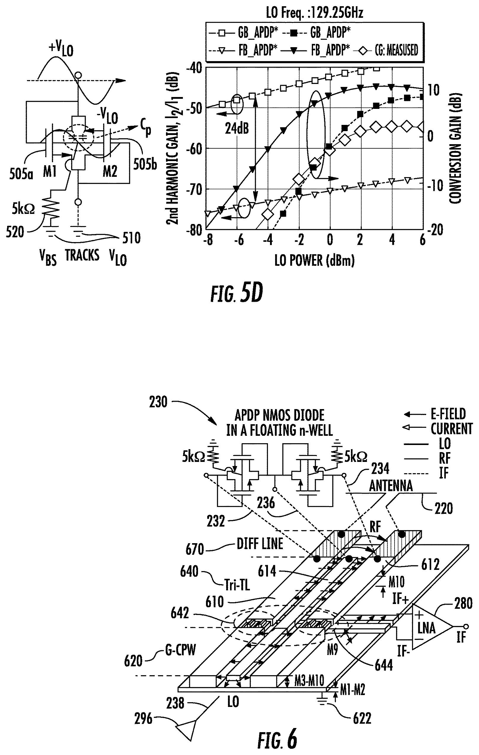
For sub-harmonic mixing, an anti-parallel diode pair (APDP) may be used because of its ability to reject even order mixed products. Although CMOS-compatible Schottky barrier diodes are available, diode-connected NMOS transistors biased in sub-threshold region may have better performance due to their symmetry in physical structure. As illustrated in FIG. 5A diode-connected transistors 505a, 505b of a grounded-body NMOS APDP (GB-APDP), through ground 510, experience different body-to source-voltage (VBS) or body effect.
Because of this, even-order harmonics are not perfectly cancelled as shown in FIG. 5B, and increased conversion loss has been observed in simulations. To avoid these, a floating-body NMOS APDP (FB-APDP) may be used.
As shown in FIG. 5C, two triple-well NMOSFETs may be used to form the APDP structure. Instead of connecting the body terminal directly to the ground, a 5-k.OMEGA. resistor 520 (or other large resistance resistor) is inserted between the ground 510 and body node to AC isolate or float the body node. In operation, a strong voltage LO will create a replica on the body terminal letting the body closely track applied LO voltage. his allows for the body voltage to track the LO drive through the parasitic coupling and the source-to-body voltages of both MOSFETs to be kept the same over an entire LO cycle. FIG. 5C also shows a conceptual substrate including a possible circuit design as discussed.
The effectiveness of floating body connection can be clearly seen through simulations results in FIG. 5D that show that the undesired second harmonic current, which can decrease sub-harmonic conversion efficiency and increase noise "folding" effect by creating strong fundamental mixing term may be rejected by more than 24 dB and at given conversion gain, and .about.4 dB lower LO power may be needed.
Wideband Hybrid
FIG. 6 shows a wideband hybrid structure 260 that provides port isolation and impedance matching over a 200-300 GHz frequency range. Conventional hybrid designs relying on .lamda./4-transmission lines are narrow-band. For designs using the wideband hybrid structure 260, RF and LO signals from the antenna 220 and LO amplifier 296 respectively are isolated by using different modes in a three-line 610, 612, 614 transmission line (Tri-TL) that simultaneously supports both even and odd mode propagation.
The hybrid structure 260 may be seen as having a grounded coplanar waveguide 620, Tri-TL 640, and differential line 660. The differential line interfaces to an on-chip differentially-fed dipole antenna operating in odd mode. The coplanar waveguide interfaces to single-ended LO chain operating in even mode. The Tri-TL supports both odd and even mode simultaneously which enables LO and RF signal mixing.
The RF signal received using a differentially fed on-chip dipole antenna 220 is delivered to the floating body anti parallel diode pair (FBAPDP) mixing core 230 in an odd mode through the Tri-TL transmission lines 610, 612, 614. As can be seen in both FIG. 2 and FIG. 6, the antenna 220 and mixing core 230 are connected to the hybrid structure transmission lines 610, 612, and 614 by lines 232, 234, and 236 respectively.
The LO amplifier 296 generates a single-ended LO signal that is fed through line 238 to a grounded coplanar waveguide (GCPW) 620 and delivered to the hybrid 260 through the Tri-TL structure 640 in even mode. Wideband isolation between RF and LO signals is achieved because the feed structure of one cannot support the mode of the other. To isolate the IF path 660 to the low noise amplifier 280 from the hard short provided by the ground 622 of the GCPW 620, two 80-fF metal oxide-metal capacitors 642, 644 may be inserted into the ground path of LO GCPW 620. This capacitance serves as a short for RF and LO signals and absorbed into an IF matching network. Since the IF signal is extracted from the node at which LO and RF signals are AC grounded, a high-Q IF matching network may be implemented without affecting the LO and RF matching. High-Q Matching network is intended to optimize the noise and power gain performance of IF LNA which would be otherwise difficult without the current configuration.
In testing, this hybrid structure 260 may provide over a 100-GHz bandwidth detection capabilities with less than 1-dB transmission loss with isolation between all ports exceeding 50 dB.
Structurally, layers M1-2 support the base structure, M3-10 support the transmission lines 610, 612 in the GCPW 620, M9 supports the IF lines IF+, IF-, and M10 supports the RF differential input from the antenna 670, and the LO line 614 at the GCPW 620, Tri-TL 640, and differential 670, and the RF lines 610, 612 at the tri-TL 640 and differential 670.
FIG. 6 graphically shows the IF signal IF, RF signal RF, LO signal LO, current Current, and e-field E-field for illustration purposes to show both isolation and connection.
While the invention has been described with reference to the embodiments above, a person of ordinary skill in the art would understand that various changes or modifications may be made thereto without departing from the scope of the claims.
* * * * *
D00000
D00001
D00002
D00003
D00004
D00005
XML
uspto.report is an independent third-party trademark research tool that is not affiliated, endorsed, or sponsored by the United States Patent and Trademark Office (USPTO) or any other governmental organization. The information provided by uspto.report is based on publicly available data at the time of writing and is intended for informational purposes only.
While we strive to provide accurate and up-to-date information, we do not guarantee the accuracy, completeness, reliability, or suitability of the information displayed on this site. The use of this site is at your own risk. Any reliance you place on such information is therefore strictly at your own risk.
All official trademark data, including owner information, should be verified by visiting the official USPTO website at www.uspto.gov. This site is not intended to replace professional legal advice and should not be used as a substitute for consulting with a legal professional who is knowledgeable about trademark law.