Passive multi-input comparator for orthogonal codes on a multi-wire bus
Tajalli , et al. A
U.S. patent number 10,742,451 [Application Number 16/435,412] was granted by the patent office on 2020-08-11 for passive multi-input comparator for orthogonal codes on a multi-wire bus. This patent grant is currently assigned to KANDOU LABS, S.A.. The grantee listed for this patent is Kandou Labs, S.A.. Invention is credited to Chen Cao, Kiarash Gharibdoust, Armin Tajalli.
View All Diagrams
| United States Patent | 10,742,451 |
| Tajalli , et al. | August 11, 2020 |
Passive multi-input comparator for orthogonal codes on a multi-wire bus
Abstract
Methods and systems are described for receiving a plurality of signals via a plurality of wires of a multi-wire bus, the plurality of signals corresponding to symbols of a codeword of a vector signaling code, generating, using an interconnected resistor network connected to the plurality of wires of the multi-wire bus, a plurality of combinations of the symbols of the codeword of the vector signaling code on a plurality of output nodes, the plurality of output nodes including a plurality of pairs of sub-channel output nodes associated with respective sub-channels of a plurality of sub-channels, and generating a plurality of sub-channel outputs using a plurality of differential transistor pairs, each differential transistor pair of the plurality of differential transistor pairs connected to a respective pair of sub-channel output nodes of the plurality of pairs of sub-channel output nodes.
| Inventors: | Tajalli; Armin (Salt Lake City, UT), Cao; Chen (Lausanne, CH), Gharibdoust; Kiarash (Lonay, CH) | ||||||||||
|---|---|---|---|---|---|---|---|---|---|---|---|
| Applicant: |
|
||||||||||
| Assignee: | KANDOU LABS, S.A. (Lausanne,
CH) |
||||||||||
| Family ID: | 67138038 | ||||||||||
| Appl. No.: | 16/435,412 | ||||||||||
| Filed: | June 7, 2019 |
Prior Publication Data
| Document Identifier | Publication Date | |
|---|---|---|
| US 20190379563 A1 | Dec 12, 2019 | |
Related U.S. Patent Documents
| Application Number | Filing Date | Patent Number | Issue Date | ||
|---|---|---|---|---|---|
| 62684538 | Jun 13, 2018 | ||||
| 62683955 | Jun 12, 2018 | ||||
| Current U.S. Class: | 1/1 |
| Current CPC Class: | H04L 25/0292 (20130101); H04L 25/0274 (20130101); H04L 25/49 (20130101); H04L 25/0278 (20130101); H04L 25/0276 (20130101); H04B 3/02 (20130101); H03M 7/20 (20130101); H03M 5/14 (20130101); H04L 25/085 (20130101) |
| Current International Class: | H04L 25/02 (20060101) |
References Cited [Referenced By]
U.S. Patent Documents
| 3636463 | January 1972 | Ongkiehong |
| 3824494 | July 1974 | Wilcox |
| 3939468 | February 1976 | Mastin |
| 4276543 | June 1981 | Miller et al. |
| 4774498 | September 1988 | Traa |
| 4897657 | January 1990 | Brubaker |
| 5017924 | May 1991 | Guiberteau et al. |
| 5459465 | October 1995 | Kagey |
| 5510736 | April 1996 | Van |
| 5748948 | May 1998 | Yu et al. |
| 5793254 | August 1998 | OConnor |
| 5945935 | August 1999 | Kusumoto et al. |
| 6226330 | May 2001 | Mansur |
| 6232908 | May 2001 | Nakaigawa |
| 6346907 | February 2002 | Dacy et al. |
| 6384758 | May 2002 | Michalski et al. |
| 6396329 | May 2002 | Zerbe |
| 6400302 | June 2002 | Amazeen et al. |
| 6462584 | October 2002 | Proebsting |
| 6563382 | May 2003 | Yang |
| 6624699 | September 2003 | Yin et al. |
| 6839587 | January 2005 | Yonce |
| 6879816 | April 2005 | Bult et al. |
| 6888483 | May 2005 | Mulder |
| 6972701 | December 2005 | Jansson |
| 7075996 | July 2006 | Simon et al. |
| 7167523 | January 2007 | Mansur |
| 7188199 | March 2007 | Leung et al. |
| 7199728 | April 2007 | Dally et al. |
| 7269212 | September 2007 | Chau et al. |
| 7285977 | October 2007 | Kim |
| 7372295 | May 2008 | Wei |
| 7372390 | May 2008 | Yamada |
| 7397302 | July 2008 | Bardsley et al. |
| 7528758 | May 2009 | Ishii |
| 7656321 | February 2010 | Wang |
| 7683720 | March 2010 | Yehui et al. |
| 7688102 | March 2010 | Bae et al. |
| 7697915 | April 2010 | Behzad et al. |
| 7804361 | September 2010 | Lim et al. |
| 7957472 | June 2011 | Wu et al. |
| 8000664 | August 2011 | Khorram |
| 8030999 | October 2011 | Chatterjee et al. |
| 8106806 | January 2012 | Toyomura et al. |
| 8159375 | April 2012 | Abbasfar |
| 8159376 | April 2012 | Abbasfar |
| 8183930 | May 2012 | Kawakami et al. |
| 8547272 | October 2013 | Nestler et al. |
| 8581824 | November 2013 | Baek et al. |
| 8604879 | December 2013 | Mourant et al. |
| 8643437 | February 2014 | Chiu et al. |
| 8674861 | March 2014 | Matsuno et al. |
| 8687968 | April 2014 | Nosaka et al. |
| 8791735 | July 2014 | Shibasaki |
| 8841936 | September 2014 | Nakamura |
| 8860590 | October 2014 | Yamagata et al. |
| 9069995 | June 2015 | Cronie |
| 9106465 | August 2015 | Walter |
| 9148087 | September 2015 | Tajalli |
| 9178503 | November 2015 | Hsieh |
| 9281785 | March 2016 | Sjoland |
| 9292716 | March 2016 | Winoto et al. |
| 9300503 | March 2016 | Holden et al. |
| 10003315 | June 2018 | Tajalli |
| 2001/0006538 | July 2001 | Simon et al. |
| 2002/0050861 | May 2002 | Nguyen et al. |
| 2002/0149508 | October 2002 | Hamashita |
| 2002/0158789 | October 2002 | Yoshioka et al. |
| 2002/0174373 | November 2002 | Chang |
| 2003/0016763 | January 2003 | Doi et al. |
| 2003/0085763 | May 2003 | Schrodinger et al. |
| 2003/0132791 | July 2003 | Hsieh |
| 2003/0160749 | August 2003 | Tsuchi |
| 2003/0174023 | September 2003 | Miyasita |
| 2003/0184459 | October 2003 | Engl |
| 2003/0218558 | November 2003 | Mulder |
| 2004/0027185 | February 2004 | Fiedler |
| 2004/0169529 | September 2004 | Afghani et al. |
| 2005/0057379 | March 2005 | Jansson |
| 2005/0270098 | December 2005 | Zhang et al. |
| 2006/0036668 | February 2006 | Jaussi et al. |
| 2006/0097786 | May 2006 | Su et al. |
| 2006/0103463 | May 2006 | Lee et al. |
| 2006/0192598 | August 2006 | Baird et al. |
| 2006/0194598 | August 2006 | Kim et al. |
| 2007/0009018 | January 2007 | Wang |
| 2007/0176708 | August 2007 | Otsuka et al. |
| 2007/0182487 | August 2007 | Ozasa et al. |
| 2007/0188367 | August 2007 | Yamada |
| 2007/0201546 | August 2007 | Lee |
| 2008/0001626 | January 2008 | Bae et al. |
| 2008/0165841 | July 2008 | Wall et al. |
| 2008/0187037 | August 2008 | Bulzacchelli et al. |
| 2009/0090333 | April 2009 | Spadafora et al. |
| 2009/0115523 | May 2009 | Akizuki et al. |
| 2009/0323864 | December 2009 | Tired |
| 2010/0148819 | June 2010 | Bae et al. |
| 2010/0156691 | June 2010 | Taft |
| 2010/0219781 | September 2010 | Kuwamura |
| 2010/0235673 | September 2010 | Abbasfar |
| 2010/0271107 | October 2010 | Tran et al. |
| 2011/0028089 | February 2011 | Komori |
| 2011/0032977 | February 2011 | Hsiao et al. |
| 2011/0051854 | March 2011 | Kizer et al. |
| 2011/0057727 | March 2011 | Cranford et al. |
| 2011/0096054 | April 2011 | Cho et al. |
| 2011/0103508 | May 2011 | Mu et al. |
| 2011/0133816 | June 2011 | Wu et al. |
| 2011/0156819 | June 2011 | Kim et al. |
| 2012/0025911 | February 2012 | Zhao et al. |
| 2012/0044021 | February 2012 | Yeh et al. |
| 2012/0133438 | May 2012 | Tsuchi et al. |
| 2013/0106513 | May 2013 | Cyrusian et al. |
| 2013/0114663 | May 2013 | Ding et al. |
| 2013/0147553 | June 2013 | Iwamoto |
| 2013/0195155 | August 2013 | Pan et al. |
| 2013/0215954 | August 2013 | Beukema et al. |
| 2013/0259113 | October 2013 | Kumar |
| 2013/0334985 | December 2013 | Kim et al. |
| 2014/0119479 | May 2014 | Tajalli |
| 2014/0176354 | June 2014 | Yang |
| 2014/0177696 | June 2014 | Hwang |
| 2014/0203794 | July 2014 | Pietri et al. |
| 2014/0266440 | September 2014 | Itagaki et al. |
| 2014/0312876 | October 2014 | Hanson et al. |
| 2015/0070201 | March 2015 | Dedic et al. |
| 2015/0146771 | May 2015 | Walter |
| 2015/0198647 | July 2015 | Atwood et al. |
| 2016/0013954 | January 2016 | Shokrollahi |
| 2016/0197747 | July 2016 | Ulrich et al. |
| 2017/0085239 | March 2017 | Yuan et al. |
| 2017/0104458 | April 2017 | Cohen et al. |
| 2017/0214374 | July 2017 | Tajalli |
| 2019/0199557 | June 2019 | Taylor et al. |
| 2018052657 | Mar 2018 | WO | |||
Other References
|
Anadigm , "Using the Anadigm Multiplier CAM", Design Brief 208, www.anadigm.com, Copyright 2002, 2002, (6 pages). cited by applicant . Schneider, J. , et al., "ELEC301 Project: Building an Analog Computer", http://www.clear.rice.edu/elec301/Projects99/anlgcomp/, Dec. 19, 1999, (9 pages). cited by applicant . Tierney, J. , "A Digital Frequency Synthesizer", Audio and Electroacoustics, IEEE Transactions, pp. 48-57, vol. 19, No. 1, Abstract, Mar. 1971, (1 page). cited by applicant . International Search Report and Written Opinion for PCT/US2019/036170, dated Aug. 19, 2019, 1-14 (14 pages). cited by applicant . Kim, Kyu-Young , et al., "8 mW 1.65-Gbps continuous-time equalizer with clock attenuation detection for digital display interface", Analog Integrated Circuits and Signal Processing, Kluwer Academic Publishers, vol. 63, No. 2, Oct. 11, 2009, 329-337 (9 pages). cited by applicant . Takahashi, Masayoshi , et al., "A 2-GHz Gain Equalizer for Analog Signal Transmission Using Feedforward Compensation by a Low-Pass Filter", IEICE Transactions on Fundamentals of Electronics, vol. E94A, No. 2, Feb. 2011, 611-616 (6 pages). cited by applicant . Wang, Hui , et al., "Equalization Techniques for High-Speed Serial Interconnect Transceivers", Solid-State and Integrated-Circuit Technology, 9th International Conference on ICSICT, Piscataway, NJ, Oct. 20, 2008, 1-4 (4 pages). cited by applicant . Palmisano, G. , et al., "A Replica Biasing for Constant-Gain CMOS Open-Loop Amplifiers", Circuits and Systems, IEEE International Symposium in Monterey, CA, May 31, 1998, 363-366 (4 pages). cited by applicant. |
Primary Examiner: Lee; Siu M
Attorney, Agent or Firm: Invention Mine LLC
Parent Case Text
CROSS-REFERENCE TO RELATED APPLICATIONS
This application claims the benefit of U.S. Provisional Application No. 62/684,538, filed Jun. 13, 2018, entitled "Passive Multi-Input Comparator for Orthogonal Codes on a Multi-Wire Bus", and claims the benefit of U.S. Provisional Application No. 62/683,955, filed Jun. 12, 2018, entitled "Passive Multi-Input Comparator for Orthogonal Codes on a Multi-Wire Bus", all of which are hereby incorporated by reference in their entirety for all purposes.
Claims
We claim:
1. An apparatus comprising: a plurality of wires of a multi-wire bus configured to carry signals corresponding to symbols of a codeword of a vector signaling code; an interconnected resistor network comprising a plurality of tunable resistors, the interconnected resistor network connected to the plurality of wires of the multi-wire bus, the interconnected resistor network configured to receive the signals corresponding to the symbols of the codeword of the vector signaling code and to responsively generate combinations of the symbols of the codeword of the vector signaling code at a plurality of output nodes, each output node of the plurality of output nodes connected to a respective two or more wires of the plurality of wires of the multi-wire bus via the plurality of tunable resistors, the plurality of output nodes grouped into a plurality of pairs of sub-channel output nodes associated with respective sub-channels of a plurality of sub-channels; and a plurality of differential transistor pairs, each differential transistor pair of the plurality of differential transistor pairs connected to a respective pair of sub-channel output nodes of the plurality of pairs of sub-channel output nodes and configured to generate a respective sub-channel output of a plurality of sub-channel outputs.
2. The apparatus of claim 1, wherein each combination of the symbols of the codeword corresponds to an addition of a respective two symbols of the codeword.
3. The apparatus of claim 1, wherein each combination of the symbols of the codeword corresponds to an average of a respective two symbols of the codeword.
4. The apparatus of claim 1, wherein the plurality of tunable resistors each have equal impedance values.
5. The apparatus of claim 1, wherein each tunable resistor of the plurality of tunable resistors comprises a parallel-resistor network configured to selectively enable one or more resistors in the parallel-resistor network to set a value of a tunable impedance of the tunable resistor.
6. The apparatus of claim 1, wherein the interconnected resistor network is configured to adjust a tunable impedance of each tunable resistor of the plurality of tunable resistors to adjust high-frequency peaking of sub-channel outputs of the interconnected resistor network.
7. The apparatus of claim 1, further comprising a plurality of mode-selection transistors configured to selectively decouple one or more wires from one or more output nodes of the plurality of output nodes.
8. The apparatus of claim 7, wherein the plurality of mode-selection transistors are configured to couple one respective wire of the plurality of wires of the multi-wire bus to a respective output node of the plurality of output nodes, and wherein each sub-channel output of the plurality of sub-channel outputs corresponds to a differential output across two wires of the plurality of wires of the multi-wire bus.
9. A method comprising: receiving a plurality of signals via a plurality of wires of a multi-wire bus, the plurality of signals corresponding to symbols of a codeword of a vector signaling code; generating, using an interconnected resistor network connected to the plurality of wires of the multi-wire bus, a plurality of combinations of the symbols of the codeword of the vector signaling code on a plurality of output nodes, each output node of the plurality of output nodes is connected to a respective two or more wires of the plurality of wires of the multi-wire bus, each wire of the respective two or more wires connected via a respective tunable resistor of a plurality of tunable resistors of the interconnected resistor network, the plurality of output nodes comprising a plurality of pairs of sub-channel output nodes associated with respective sub-channels of a plurality of sub-channels; and generating a plurality of sub-channel outputs using a plurality of differential transistor pairs, each differential transistor pair of the plurality of differential transistor pairs connected to a respective pair of sub-channel output nodes of the plurality of pairs of sub-channel output nodes.
10. The method of claim 9, wherein generating the plurality of combinations of the symbols of the codeword comprises adding a respective two or more signals corresponding to a respective two or more symbols of the codeword.
11. The method of claim 9, wherein generating the plurality of combinations of the symbols of the codeword comprises forming an average of a respective two or more signals corresponding to a respective two or more symbols of the codeword.
12. The method of claim 9, wherein the plurality of tunable resistors each have equal impedance values.
13. The method of claim 9, wherein each tunable resistor of the plurality of tunable resistors comprises a parallel-resistor network, and wherein the method further comprises selectively enabling one or more resistors in the parallel-resistor network to set an impedance value of a tunable impedance of the tunable resistor.
14. The method of claim 9, further comprising adjusting high-frequency peaking of the plurality of sub-channel outputs by adjusting tunable impedance of the plurality of tunable resistors.
15. The method of claim 9, further comprising selecting an operational mode via a plurality of mode-selection transistors, the plurality of mode-selection transistors selectively decoupling one or more wires from one or more output nodes of the plurality of output nodes.
16. The method of claim 15, further comprising coupling one respective wire of the plurality of wires of the multi-wire bus to a respective output node of the plurality of output nodes, and wherein each sub-channel output of the plurality of sub-channel outputs corresponds to a differential output across two wires of the plurality of wires of the multi-wire bus.
Description
REFERENCES
The following prior applications are herein incorporated by reference in their entirety for all purposes:
U.S. Pat. No. 9,288,089, filed May 20, 2010 as application Ser. No. 12/784,414 and issued Mar. 15, 2016, naming Harm Cronie and Amin Shokrollahi, entitled "Orthogonal Differential Vector Signaling", hereinafter identified as [Cronie].
U.S. patent application Ser. No. 13/842,740, filed Mar. 15, 2013, naming Brian Holden, Amin Shokrollahi, and Anant Singh, entitled "Methods and Systems for Skew Tolerance in and Advanced Detectors for Vector Signaling Codes for Chip-to-Chip Communication", hereinafter identified as [Holden].
U.S. Pat. No. 9,100,232, filed Feb. 2, 2015 as application Ser. No. 14/612,241, and issued Aug. 4, 2015, naming Ali Hormati, Amin Shokrollahi, and Roger Ulrich, entitled "Method for Code Evaluation using ISI Ratio", hereinafter identified as [Hormati I].
U.S. patent application Ser. No. 15/582,545, filed Apr. 28, 2017, naming Ali Hormati and Richard Simpson, entitled "Clock Data Recovery with Decision Feedback Equalization" hereinafter identified as [Hormati II].
BACKGROUND
In communication systems, a goal is to transport information from one physical location to another. One common information transfer medium is the serial communications link, which may be based on a single wire circuit relative to ground or other common reference, multiple such circuits relative to ground or other common reference, or multiple circuits used in relation to each other. A common example of the latter uses differential signaling ("DS"). Differential signaling operates by sending a signal on one wire and the opposite of that signal on a matching wire. The signal information is represented by the difference between the wires, rather than their absolute values relative to ground or other fixed reference. Vector signaling is another such example. With vector signaling, a plurality of signals on a plurality of wires are considered collectively, although each of the plurality of signals might be independent. With binary vector signaling, each component or "symbol" of the vector takes on one of two possible values. With non-binary vector signaling, each symbol has a value that is a selection from a set of more than two possible values. Any suitable subset of a vector signaling code denotes a "subcode" of that code. Such a subcode may itself be a vector signaling code.
BRIEF DESCRIPTION
A detection matrix is described for an Orthogonal Differential Vector Signaling code in which passive resistor networks are used to sum at least some of the input terms of that code before active detection of a subchannel result. Such passive summation can reduce the detrimental effects of common mode signal variation and increase the dynamic range of the resulting detector.
Methods and systems are described for receiving a plurality of signals via a plurality of wires of a multi-wire bus, the plurality of signals corresponding to symbols of a codeword of a vector signaling code, generating, using an interconnected resistor network connected to the plurality of wires of the multi-wire bus, a plurality of combinations of the symbols of the codeword of the vector signaling code on a plurality of output nodes, the plurality of output nodes including a plurality of pairs of sub-channel output nodes associated with respective sub-channels of a plurality of sub-channels, and generating a plurality of sub-channel outputs using a plurality of differential transistor pairs, each differential transistor pair of the plurality of differential transistor pairs connected to a respective pair of sub-channel output nodes of the plurality of pairs of sub-channel output nodes.
BRIEF DESCRIPTION OF FIGURES
FIG. 1 is a circuit diagram of an ODVS subchannel detector incorporating a passive multi-input comparator (MIC), in accordance with some embodiments.
FIG. 2 is a schematic of an interconnected resistor network in a passive MIC, in accordance with some embodiments.
FIG. 3 is a circuit diagram of a tunable resistor array for selectively enabling a number of resistive elements, in accordance with some embodiments.
FIGS. 4-6 are schematics of sub-channel specific portions of the interconnected resistor network configurable to operate in a multi-mode system, in accordance with some embodiments.
FIG. 7 is a schematic of the interconnected resistor network including switching devices for operating in a multi-mode system, in accordance with some embodiments.
FIG. 8 is a flowchart of a method, in accordance with some embodiments.
FIG. 9 is a block diagram of for configuring a transceiver in a Tx or RX mode of operation, in accordance with some embodiments.
FIG. 10 is a block diagram of a transceiver operating in a full-duplex mode of operation, in accordance with some embodiments.
FIG. 11 is a circuit schematic of a switch used in the tunable resistor array, in accordance with some embodiments.
DETAILED DESCRIPTION
Orthogonal Differential Vector Signaling codes (ODVS) are described [Cronie] as being particularly suited to use in high-speed multiwire communication systems. In one interpretation, ODVS is described as a word-oriented encoding/decoding method providing improved performance and robustness; data words are encoded into ODVS codewords for transmission essentially in parallel on multiple signal wires, one such codeword per unit interval, with the receiver subsequently detecting those codewords and decoding them so as to recover the data. In an alternative view, each ODVS codeword may be interpreted as a weighted summation of multiple independent (e.g. orthogonal) sub-channel vectors, each sub-channel vector modulated by a corresponding data signal of the overall data word composed of multiple data signals being transmitted.
In some embodiments, an ODVS code is described and defined by a matrix. Each row of the matrix may be interpreted as a sub-channel vector of elements that may be weighted by a corresponding signal element, with each column representing one wire of the multiwire communications channel. An individual wire signal may thus contribute to multiple sub-channels in various combinations with other wire signals.
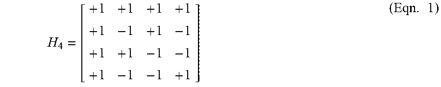
Without implying limitation, the H4 code of [Cronie], also known as the Ensemble Non-Return-to-Zero or ENRZ code, will be used in the subsequent examples. ENRZ encodes three data bits for transmission over a four-wire channel. Its defining matrix is:
.times. ##EQU00001## and encoding of the three bits D.sub.0, D.sub.1, D.sub.2 may be obtained by multiplying the data bits by rows 2-4 of the Hadamard matrix H4 to obtain four output values. In such an embodiment, each row of the rows 2-4 of the matrix of Eqn. 1 corresponds to a respective sub-channel vector of a plurality of sub-channel vectors. Each sub-channel vector being modulated, or weighted, by a respective data bit (taking values of +1 or -1) corresponds to a modulated sub-channel. A sum of all of the modulated sub-channels produces a codeword of a vector signaling code. In the word-oriented view, the three-bit data word D<2:0> is multiplied by rows 2-4 of the above matrix to encode the data into a four value codeword composed of values [A, B, C, D]. An offset may be added to each codeword value for ease in transmission along the multi-wire bus medium. Because the first "all-ones" row of the matrix is not used, the resulting codewords of the ENRZ code are balanced, all symbols of a given codeword summing to zero (or a constant when an offset is added), and are either permutations of the vector [+1, -1/3, -1/3, -1/3] or [-1, +1/3, +1/3, +1/3]. Thus, physical wire signals corresponding to a series of ENRZ codewords may take on four distinct values.
In some embodiments, the uppermost vector of the matrix is described as corresponding to common mode signaling, which is not used herein. Thus, each of the sub-channel vectors corresponding to rows 2-4 of the matrix are multiplied (or modulated) by a corresponding data bit of the set of data bits D.sub.0, D.sub.1, D.sub.2 to produce three modulated sub-channels, which are summed together to produce symbols A, B, C, D, of the codeword to transmit over wires of a multi-wire bus.
As described by [Cronie], ODVS may be decoded by multiplication of the received signals by a decoding matrix. In some embodiments, the decoding matrix may correspond to the encoding matrix, or alternatively an inverse of the encoding matrix. As described in [Cronie], "Sylvester Hadamard matrices" are symmetric, which means they are identical to their inverses. [Holden] further teaches that one efficient means of performing this operation uses Multi-Input Comparators (MICs). Each MIC computes a linear combination of weighted input signals where the weights at a given MIC are determined by a corresponding sub-channel vector in the detection matrix, with the output of each MIC corresponding to an antipodal sub-channel output representing the input data at the transmitter. Thus, binary data encoded onto an ENRZ channel will result in an antipodal (i.e. a single "eye" opening) MIC output that may be sampled using conventional binary signal detection methods. A set of MICs that detect the plurality of ENRZ sub-channels may be described by equations 2-4 below: Sub.sub.0=(W1+W3)-(W0+W2) (Eqn. 2) Sub.sub.1=(W0+W3)-(W1+W2) (Eqn. 3) Sub.sub.2=(W2+W3)-(W0+W1) (Eqn. 4)
where wire signals W0, W1, W2, W3 represent individual columns [Holden] further teaches that these equations may be efficiently implemented in analog logic as three instances of a four-input differential amplifier, the described embodiment having multiple transistor inputs producing two inverting and two non-inverting terms of equal weight that are actively summed to the desired result.
MIC embodiments that rely on active input elements may have issues with signal dynamic range and/or common mode rejection. The latter may be a significant problem with ODVS codes such as ENRZ, as modulation of one subchannel can present as a varying common mode offset in other sub-channels.
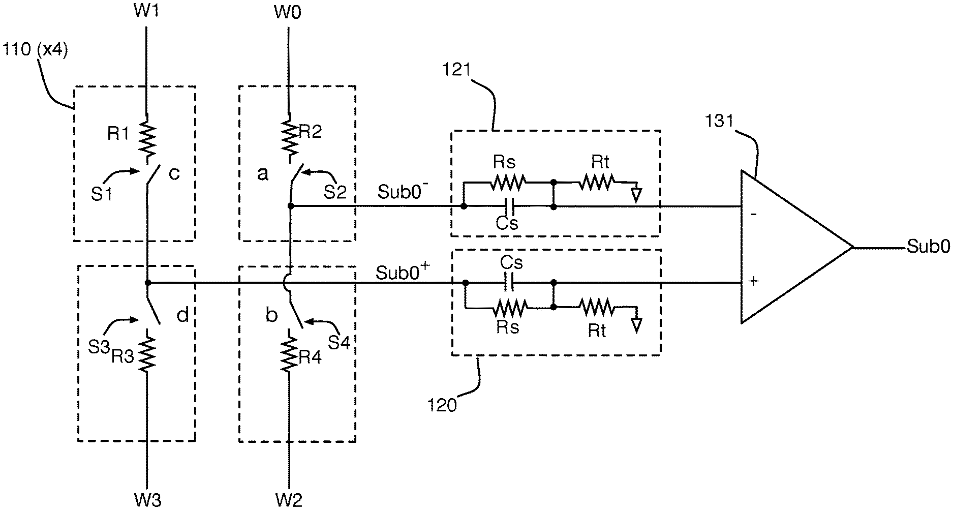
A passive MIC embodiment is presented which avoids these issues. Rather than using active circuit components to buffer and isolate the input signals before the analog computation, a passive interconnected resistor network performs the combinations of the symbols of the codeword on a plurality of pairs of sub-channel output nodes prior to a conventional differential signal receiver or amplifier. In at least one embodiment, an interconnected resistor network may include three identical instances of a resistor network each being driven by a respective input permutation of input signals to provide differential outputs on a respective pair of sub-channel output nodes that are provided to respective signal receivers/differential amplifiers, which in turn generate three sub-channel outputs. FIG. 1 is a schematic of one particular sub-channel receiver for detecting one sub-channel of the example ENRZ code, in accordance with some embodiments.
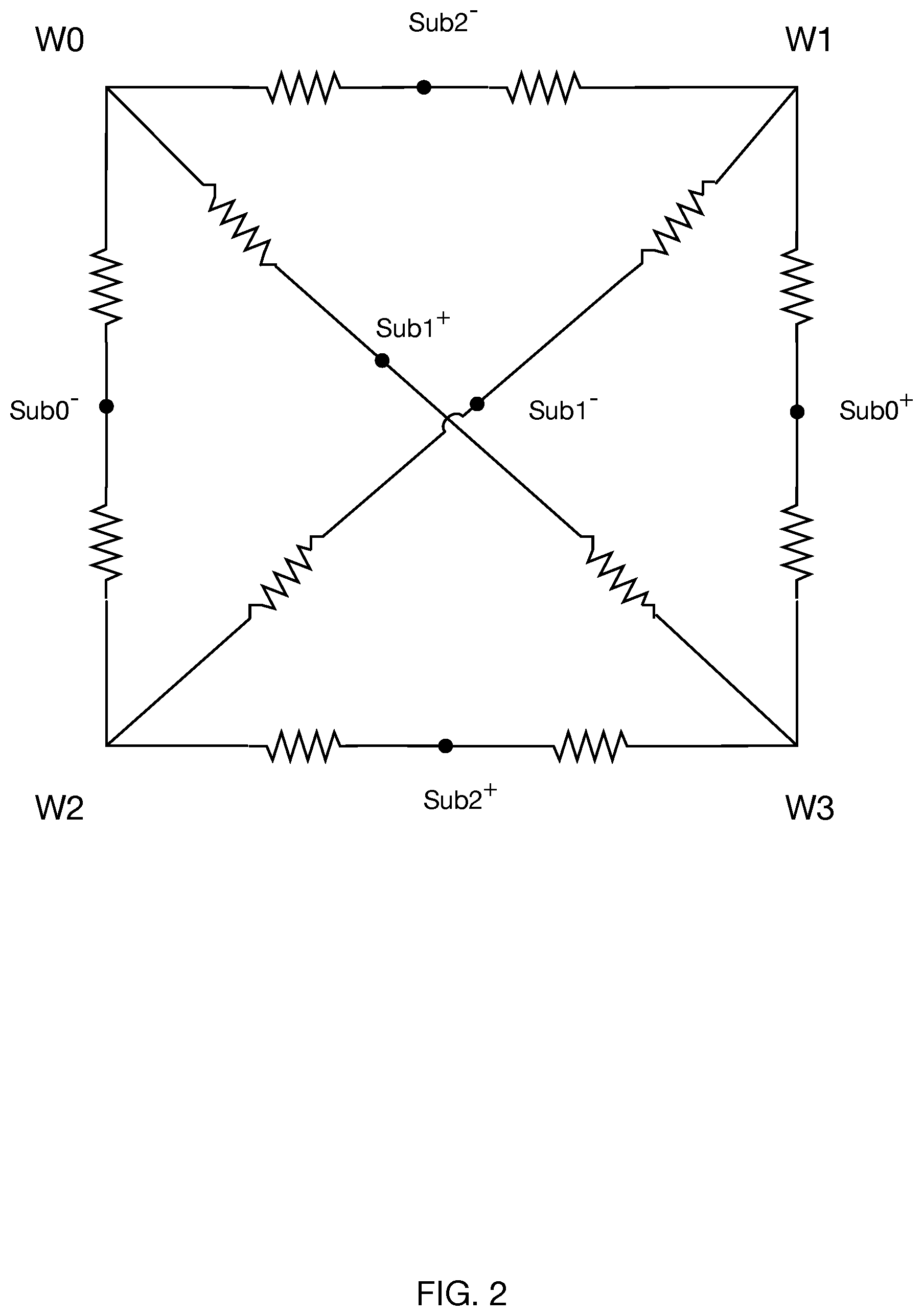
FIG. 2 illustrates an interconnected resistor network in accordance with some embodiments. As shown, the interconnected resistor network is connected to a plurality of wires of a multi-wire bus carrying signals corresponding to symbols of a codeword of a vector signaling code. In the description below, the notation W0-W3 may correspond to the wires of the multi-wire bus, the wire signals carried on said wires, or may be used to refer to the symbols of the codeword of the vector signaling code. The interconnected resistor network is configured to receive the wire signals corresponding to the symbols of the codeword of the vector signaling code and to responsively generate combinations (e.g., combination of symbols Sub.sub.0.sup.+) of the symbols of the codeword of the vector signaling code on a plurality of output nodes. As shown in FIG. 2, the plurality of output nodes includes a plurality of pairs of sub-channel output nodes associated with respective sub-channels of a plurality of sub-channels. The pair of output nodes Sub.sub.0.sup.+ and Sub.sub.0.sup.- are grouped to form a pair of sub-channel output nodes for sub-channel Sub.sub.0, while pairs of output nodes Sub.sub.1.sup.-/Sub.sub.1.sup.- and Sub.sub.2.sup.+/Sub.sub.2.sup.- are grouped to form pairs of sub-channel output nodes for sub-channels Sub.sub.1 and Sub.sub.2, respectively as defined above in Eqns. 2-4. The interconnected resistor network is connected to a plurality of differential transistor pairs (e.g., respective instances of differential amplifier 131 in FIG. 1), each differential transistor pair of the plurality of differential transistor pairs connected to a respective pair of sub-channel output nodes of the plurality of pairs of sub-channel output nodes and configured to generate a respective sub-channel output of a plurality of sub-channel outputs.
FIG. 1 is a block diagram of a sub-channel receiver configured for detecting sub-channel Sub.sub.0, in accordance with some embodiments. In FIG. 1, the wire signals are labeled W0, W1, W2, W3, corresponding to the symbols of the codeword A, B, C, D of, in this example, sub-channel Sub.sub.0 defined by Eqn. 2. In at least one embodiment, the wire signals are received without additional amplification or signal processing. In other embodiments, the wire signals may be the outputs of conventional variable gain amplifiers (VGA), continuous-time linear equalizers (CTLE), or other active processing elements.
As a first example of ENRZ detection of subchannel Sub.sub.0 with the circuit of FIG. 1, switches S1, S2, S3, S4 in series with resistors R1, R2, R3, R4 are all presumed to be closed. In some embodiments, the resistors R1-R4 are all equal valued. In some embodiments, the impedance values of resistors R1-R4 may be tunable, as illustrated in FIG. 3 and described in more detail below. Input signals on wires W1 and W3 are passively summed by resistors R1 and R3 to produce a combination of symbols Sub.sub.0.sup.+ on a first output node of a pair of sub-channel output nodes associated with sub-channel Sub.sub.0, and input signals on wires W0 and W2 are passively summed by resistors R2 and R4 to produce a combination of symbols Sub.sub.0.sup.- on a second output node of the pair of sub-channel output nodes associated with sub-channel Sub.sub.0. The combination of symbols Sub.sub.0.sup.+ may be passed through filtering circuit 120 to the positive or non-inverting input of differential amplifier 131, and the combination of symbols Sub.sub.0.sup.- is passed through filtering circuit 121 to the negative or inverting input of differential amplifier 131. In the scenario where the value of each of resistors R1, R2, R3, R4 is equal, the signals are summed with equal weights. It should be noted that using unequaled value may provide a summation using unequal weights in the scenario where a matrix having multiple magnitudes of weights is used. [Hormati I] discloses some such matrices having multiple magnitudes of weights, e.g., the Glasswing matrix.
Identical filtering circuits 120 and 121, shown here as being composed of elements Rs and Cs, connected to a termination resistor Rt, provides frequency-dependent filtering and signal termination, in accordance with some embodiments. In one example embodiment, the combination of input series impedance (e.g. R1 paralleled with R3, etc.), Rs, and Cs provide a high frequency peaking effect. while Rt provides a termination impedance for the input signal. Such filtering may be useful for clock and data recovery or CTLE, where rounded (e.g., low-pass filtered) transitions are desirable to use transition samples for generating a phase-error signal used to update a voltage-controlled oscillator (VCO). The CDR disclosed in [Hormati II] utilizing DFE may benefit from such filtering to provided more rounded eyes when utilizing speculative DFE samples as phase error information. In some embodiments, by adjusting the impedances of resistors R1-R4, the cutoff frequency of the low-pass filter may be adjusted, as described in more detail below with respect to FIG. 3.
In one embodiment, 131 is a differential linear amplifier performing the subtraction operation of Eqn. 2, thus sub-channel output Sub.sub.0 is an analog signal representing a respective data signal provided to the transmitter. In another embodiment, 131 is a differential comparator performing the subtraction operation by generating an analog antipodal value followed by an amplitude slicing operation, resulting in a binary digital sub-channel output corresponding to the binary data value used to modulate the sub-channel. In further embodiments, 131 may additionally incorporate clocked or dynamic sampling elements, capturing the state of the analog or digital result at a desired time.
The circuit of FIG. 1 acts as a multi-mode sub-channel receiver configurable for operating in various modes in addition to the ODVS mode previously described. For example, in a second or "legacy" mode, the circuit of FIG. 1 may be configured to operate as a legacy differential receiver data detector. Such an embodiment may be configured by closing switches S1 and S2 (via control signals c and a respectively) and opening switches S3 and S4 (via control signals d and b respectively); thus, signals Sub.sub.0.sup.+ and Sub.sub.0.sup.- reflect only wire signals W0 and W1, which are used as a conventional differential signal pair.
In some embodiments, the circuit may operate in a third mode, where all of the switches S1, S2, S3, S4 are opened to isolate wires W0, W1, W2, W3 from the loading effects of the subchannel receiver. Such a configuration may be used for example during a transmit (Tx) mode of operation in which other system components drive the wires in the opposite direction. In such an embodiment, every sub-channel receiver may be fully disconnected from the wires of the multi-wire bus. Alternatively, a single sub-channel receiver may be disconnected from the multi-wire bus, while the other two sub-channel receivers operate on respective differential signals, as described above.
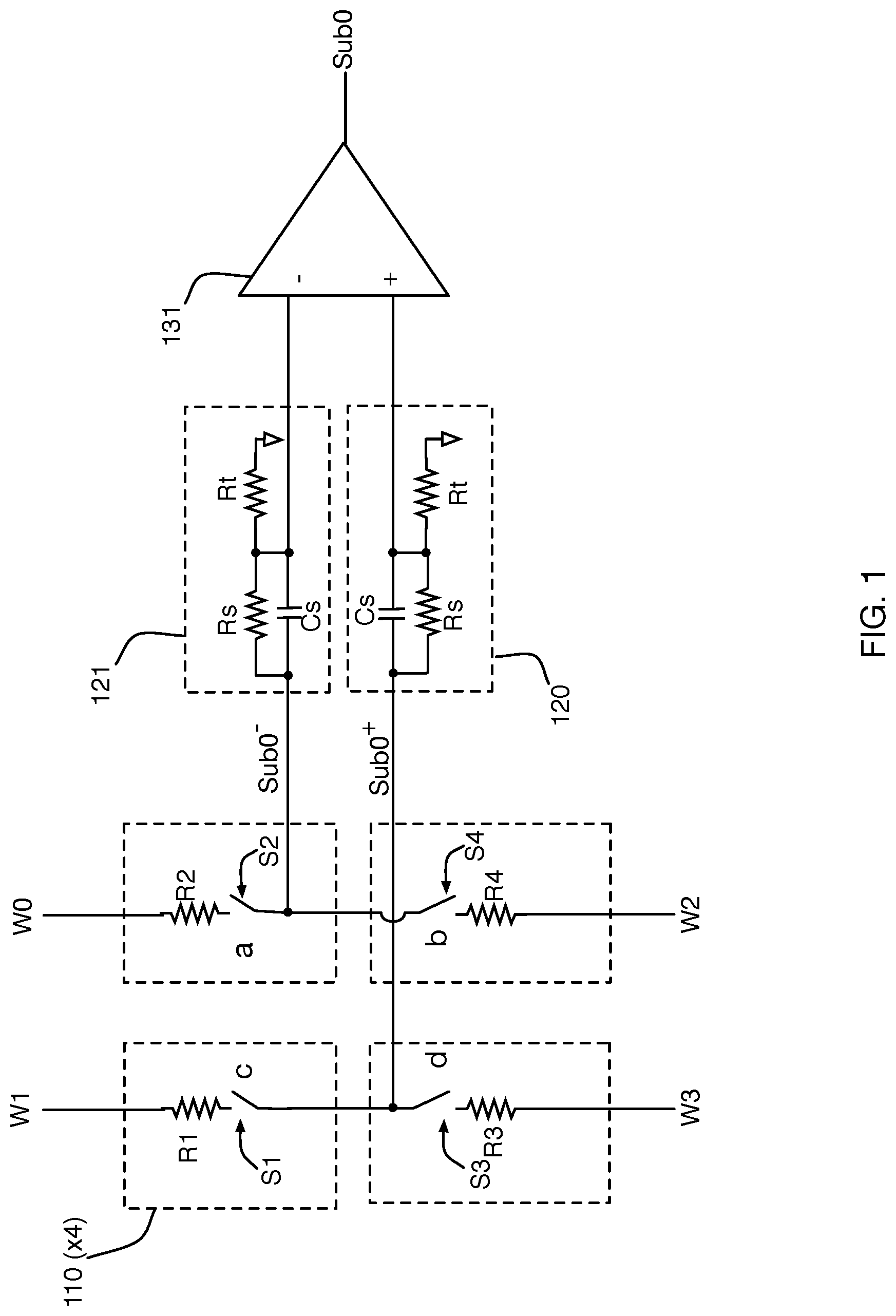
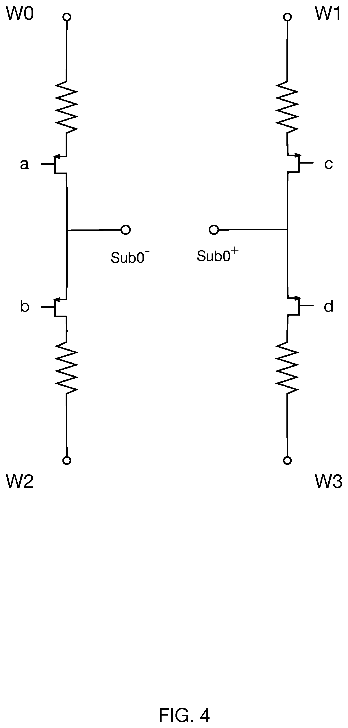
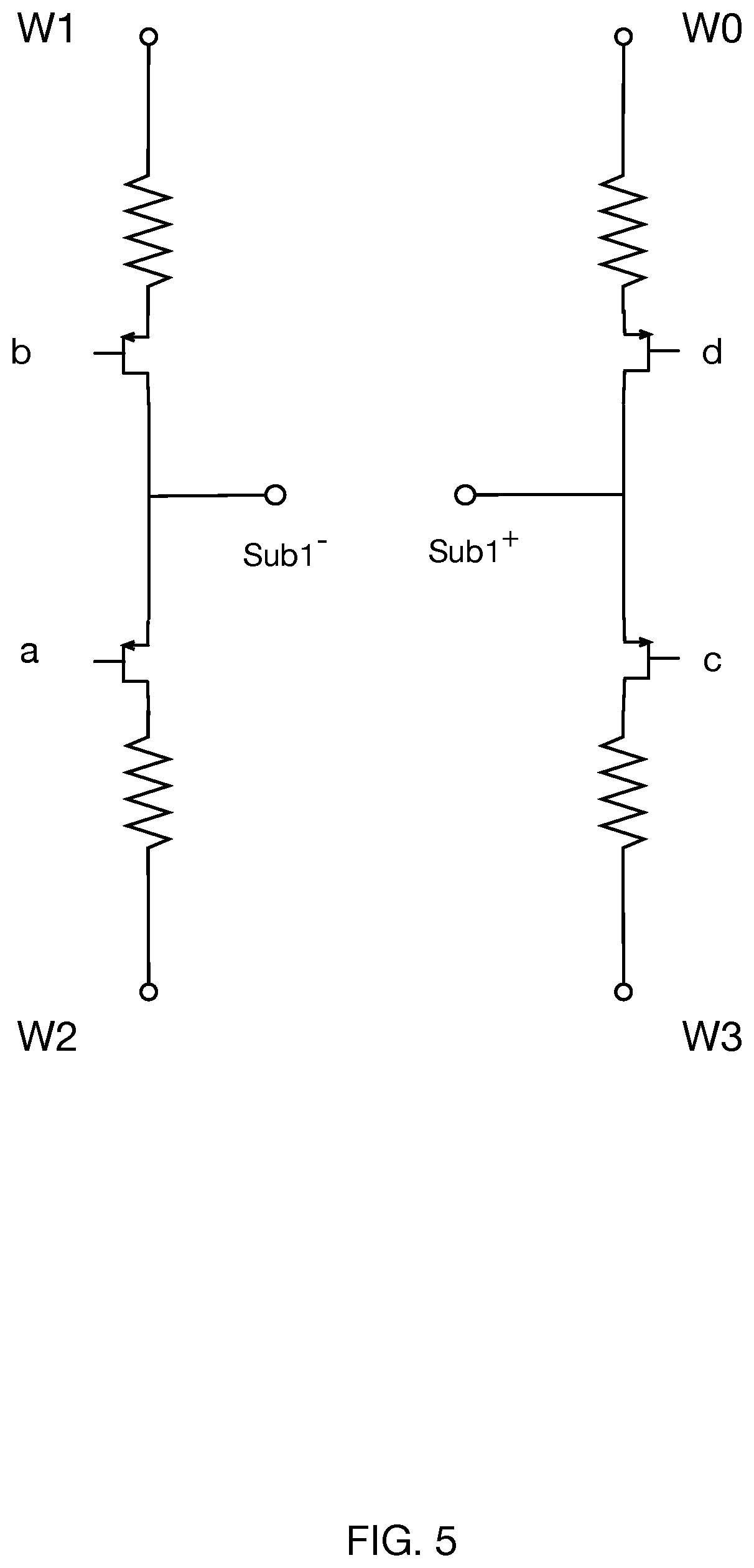
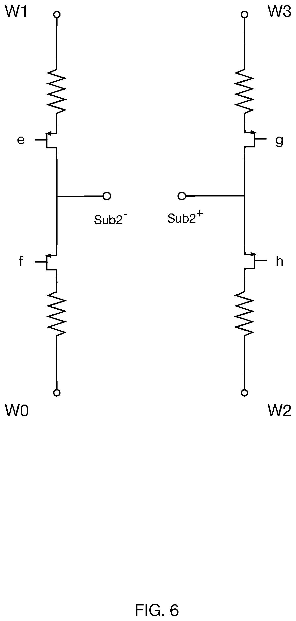
Typically, switches S1, S2, S3, S4 are implemented using MOS transistors controlled by digital mode control signals e.g., a,b,c,d as well known in the art. The schematics of FIGS. 4-6 exemplify such embodiments. In some environments multiple-transistor transmission gates may be preferred instead of MOS transistors to provide additional signal headroom or reduced distortion. The sub-channel receivers of FIG. 1 and the resistor networks in FIGS. 4-6 include switches for supporting multiple modes of operation, however, some embodiments may omit such switches by shorting the terminals connected to the switches, such as the interconnected resistor network of FIG. 2.
Sub-channel receivers for subchannels Sub.sub.1 and Sub.sub.2 may be identical to FIG. 1 except for the order in which wire signals are connected to input resistors. As illustrated in FIG. 5, Sub.sub.1 combines wire signals corresponding to symbols on wires W0 and W3 be combined to produce interim signal Sub.sub.1.sup.+ and W1 and W2 be combined to produce Sub.sub.1.sup.-. Similarly, FIG. 6 illustrates that wire signals corresponding to symbols on wires W2 and W3 produce Sub.sub.2.sup.+, and W0 and W1 to produce Sub.sub.2.sup.-.
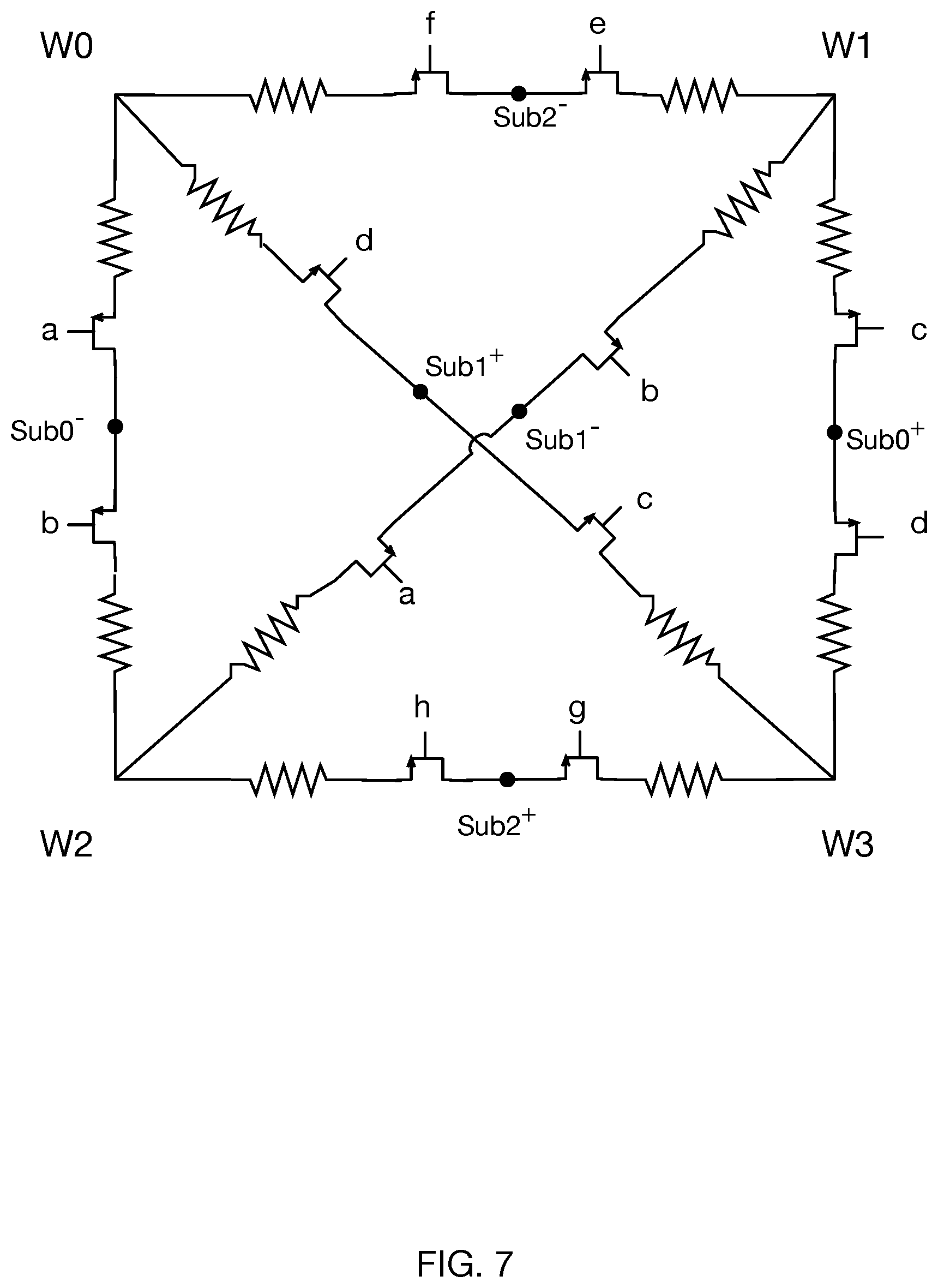
FIGS. 4-6 illustrate resistor and switching networks for sub-channels Sub.sub.0-2, respectively. As shown, each resistor network receives mode control signals to control corresponding switches. In the following example, all three sub-channel receivers may operate in either an ODVS mode where wire signals are combined on pairs of sub-channel output nodes, or alternatively a "legacy" mode may be initiated, in which sub-channel receivers Sub0 and Sub1 are configured to receive respective differential pairs signals, and sub-channel receiver Sub2 is turned off (e.g., disconnected from the bus). Table I below defines two such operation modes. In the first mode, all switches are enabled, and the pairs of sub-channel output nodes produce sub-channel outputs corresponding to detected ODVS sub-channels in accordance with Eqns. 2-4 described above. In the second mode, switches controlled by mode control signals a and c are enabled, and all other switches are disabled. In such an embodiment, a differential output between the wire signals on wires W1 and W0 is generated on the pair of sub-channel output nodes associated with sub-channel Sub0 and a differential output between the wire signals on wires W3 and W2 is generated on the pair of sub-channel output nodes associated with sub-channel Sub1. FIG. 7 illustrates the interconnected resistor network of FIG. 2 additionally including the mode selection switches for enabling multi-mode operation. In a third mode, or Tx mode, the entire interconnected resistor network is disconnected to isolate the receive circuitry, and transmit drivers are connected to the wires. In a fourth mode, or full duplex mode, the interconnected resistor network is connected to two wires of the multi-wire bus to obtain a differential signal, while the remaining two wires may be connected to transmit drivers to transmit a differential signal. Table I below and FIGS. 9-10 illustrate such further modes.
TABLE-US-00001 TABLE I Control Signal Configuration Sub.sub.0.sup.+ - Sub.sub.0.sup.- Sub.sub.1.sup.+ - Sub.sub.1.sup.- Sub.sub.2.sup.+ - Sub.sub.2.sup.- a = b = c = d = e = (W1 + W3) - (W0 + W2) (W0 + W3) - (W1 + W2) (W2 + W3) - (W0 + W1) f = g = h = `1` a = c = `1`; W1 - W0 W3 - W2 N/A b = d = e = f = g = h = `0` a = b = c = d = e = N/A N/A N/A f = g = h = `0`; (Tx Mode) (Tx Mode) (Tx Mode) i = j = k = l = `1` a = c = k = l = `1`; W1 - W0 N/A N/A b = d = e = f = g = h = (Full Duplex) (Full Duplex) (Full Duplex) i = j = m = n = `0`
In some embodiments, as described above, the interconnected resistor network is part of a transceiver that includes multiple drivers for driving symbols onto the wires of the multi-wire bus. In such an embodiment, the drivers and interconnected resistor network may be selectively connected to the multi-wire bus in a Tx mode, or one of the multiple Rx modes described above, e.g., ODVS and differential signaling or "legacy" mode. FIG. 9 is a block diagram of a transceiver 900, in accordance with some embodiments. As shown, the transceiver 900 includes a plurality of transmit drivers 905, and an interconnected resistor network 915 as previously described. In some embodiments, transceiver 900 may further include an encoder (not shown) configured to receive a set of input data and to responsively provide control signals to the drivers to generate the symbols of the codeword of the vector signal code on the multi-wire bus. The transceiver further includes a mode controller 920 that may be used to provide the multi-bit mode control signal based on a selected mode. In the transceiver 900 of FIG. 9, the multi-bit mode control signal is composed of 8 signals a-h used to control the switches in interconnected resistor network 915 as described above and shown in FIG. 7, as well as four additional signals i, j, k, l that are provided to a set of driver switches 910. In some embodiments, each signal i-l may be provided to a respective driver switch that is configured to connect or disconnect a corresponding driver to the corresponding wire of the multi-wire bus. Specifically, signal i may be provided to the driver associated with wire W0; signal j may be provided to the driver associated with wire W1; signal k may be provided to the driver associated with wire W2; and signal 1 may be provided to the driver associated with wire W3. Table I includes two additional modes utilizing such driver mode control signals. In a full Tx mode, the interconnected resistor network 915 may be fully disconnected from the multi-wire bus, while each driver is connected to a respective wire, and wire signals are driven onto the multi-wire bus. In some embodiments, a full-duplex mode may be configured, in which an inbound differential signal received via wires W0 and W1 is compared, and outbound signals are transmitted on wires W2 and W3 via the corresponding transmit drivers. Such an embodiment may utilize additional mode control signals, as control signals a and c would not be re-usable in the configuration shown in FIG. 7. In such embodiments, the MOS switches connecting wires W2 and W3 to sub-channel output nodes Sub.sub.1.sup.- and Sub.sub.1.sup.+ respectively, may receive control signals m and n. FIG. 10 illustrates a configuration of driver switches 910 utilizing 4 mode control signals i-l and an interconnected resistor network 1015 utilizing 10 mode control signals a-h, m, n for operating in such a full-duplex mode.
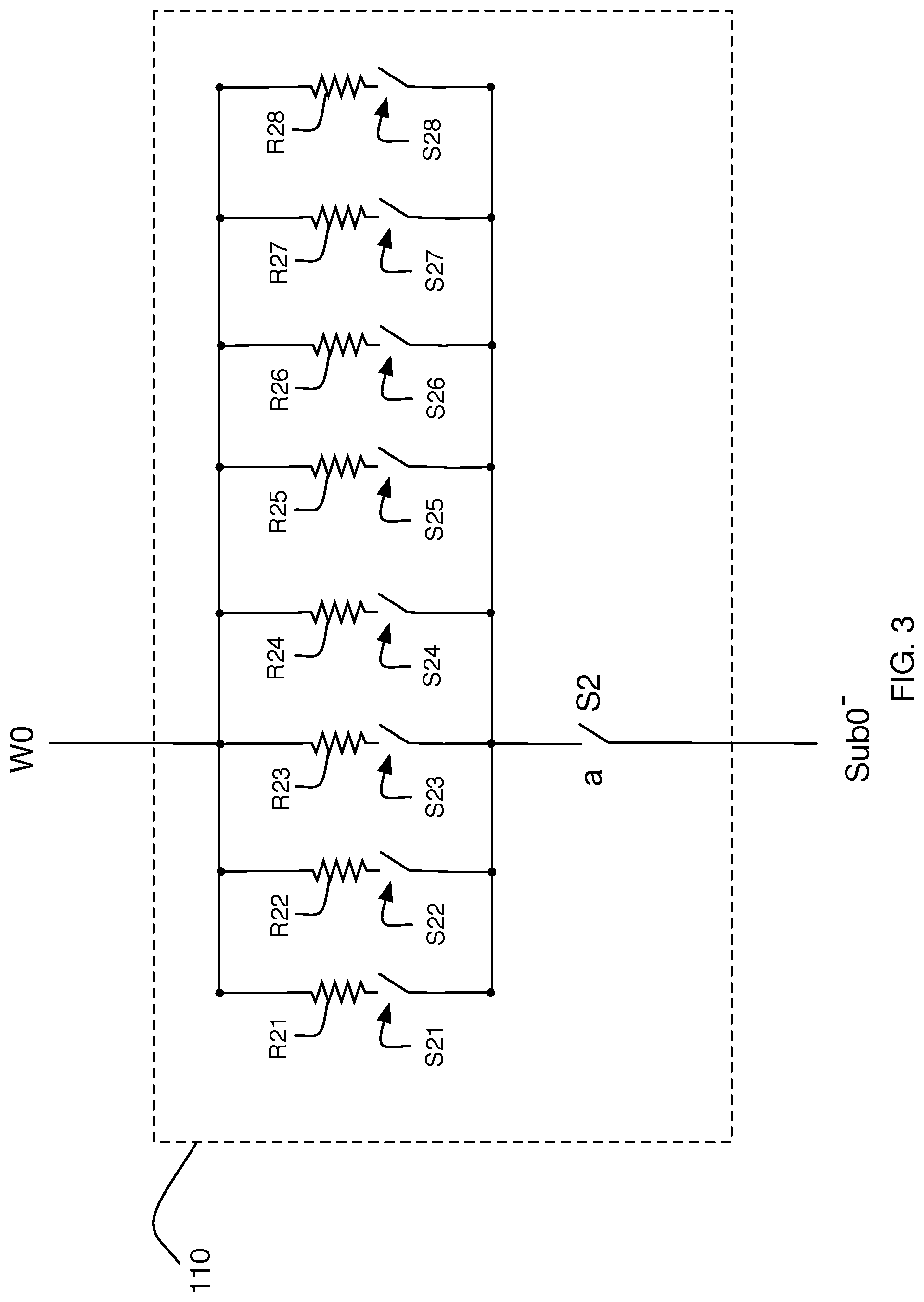
In some embodiments, the amount of high frequency peaking provided by circuit 121 may be varied by changing the effective input series impedance of the wire signals. In one particular further embodiment, each of the resistor/switch combinations 110 of FIG. 1 (one example being R1 and S1,) are embodied as multiple paralleled sets of series resistors and switches as illustrated in FIG. 3. As one example offered without limitation, resistors R21 through R28 are each of value 8*R1, with each of switches S21 through S28 being a controllable MOS transistor switch. In this embodiment, enabling from one to eight of the collection of switches S21 through S28 produces eight distinct values of effective series resistance for the overall assembly 110, producing eight distinct high frequency peaking characteristics for the combined ENRZ subchannel detector. In a practical embodiment, each instance of 110 in FIG. 1 is replaced by an instance of FIG. 3; the number of switches closed in a given instance of FIG. 3 may be zero (to disconnect that input in the second or third operational modes, as subsequently described) or a predetermined value to provide the desired frequency characteristics associated with a determined impedance value. Adjustment of the resistor value to attenuate high-frequency signal may be useful in baud-rate clock data recovery (CDR) applications, and bandwidth may be reduced if channel loss is low. Since the front-end may be shared between the Rx and the Tx, the passive MIC may completely isolate Rx from Tx by disconnecting all switches, which may increase frequency response. In some embodiments, a secondary protection device composed of a diode and a resistor (often referred to as a charged device model (CDM) diode and resistor) used to protect the system from CDM failures may be replaced by a single CDM diode, which may increase the frequency response.
In some embodiments, switching circuit S2 in resistor circuit 110 may be controlled using a single mode control bit a to set an operational mode, as shown in FIG. 1. Additionally, resistor circuit 110 may include a tunable impedance including a plurality of parallel switched-resistor circuits as show in FIG. 3, where switches S21-S28 are controlled by a multi-bit impedance control signal to set an impedance value of R2, and the mode switch controlled by mode control signal a sets the operation mode. In some embodiments, the control signals provided to S21-S28 may be logically ANDed with mode control signal a, so that the impedance value only connects wire W0 to the output node depending on the mode set by the mode control signal a.
FIG. 11 is a circuit schematic of a switch, e.g., switch S21, in accordance with some embodiments. As shown in FIG. 11, the switch is composed of NMOS transistors embedded in a P well and further using a deep N well (DNW). In such embodiments, the parasitic capacitance of the switches in resistor network may be isolated from the matching network, which would result in less loss in the Tx.
In other embodiments, digitally controlled resistor and/or capacitor groups used to adjust the frequency characteristics of 120 and 121 may be used either alone or in combination with the previously described embodiment.
In embodiments where the circuit of FIG. 3 is incorporated to change the effective input series impedance, the number of switches closed in each instance of FIG. 3 may be the same across all instances and all subchannel receivers, except for instances where all switches are open, as in the case of fully disconnecting the pair of sub-channel output nodes associated with sub-channel Sub.sub.2 in the "legacy" mode of operation as previously described.
Detection of other ODVS codes may be accomplished by adjustment of input resistor values to produce other input weighting ratios as described in [Holden]. In system environments where both true and compliment versions of input signals are available (as one example, from active CTLE stages having differential outputs,) both non-inverted and inverted signal values may be resistively summed prior to active detection.
FIG. 8 is a flowchart of a method 800, in accordance with some embodiments. As shown, method 800 includes receiving 802 a plurality of signals via a plurality of wires of a multi-wire bus, the plurality of signals corresponding to symbols of a codeword of a vector signaling code. A plurality of combinations of the symbols of the codeword of the vector signaling code are generated 804 using an interconnected resistor network connected to the plurality of wires of the multi-wire bus. The plurality of combinations of the symbols of the codeword of the vector signaling code are generated on a plurality of output nodes, where the plurality of output nodes are grouped to form a plurality of pairs of sub-channel output nodes associated with respective sub-channels of a plurality of sub-channels. A plurality of sub-channel outputs are generated 806 using a plurality of differential transistor pairs, each differential transistor pair of the plurality of differential transistor pairs connected to a respective pair of sub-channel output nodes of the plurality of pairs of sub-channel output nodes.
In some embodiments, the plurality of combinations of the symbols of the codeword are generated by adding two or more signals corresponding to the symbols of the codeword. In some embodiments, the plurality of combinations of the symbols of the codeword are generated by forming an average of two or more signals corresponding to the symbols of the codeword.
In some embodiments, each output node of the plurality of output nodes is connected to two or more wires of the plurality of wires of the multi-wire bus via respective resistors of a plurality of resistors, as shown in FIG. 2. In some embodiments, the plurality of resistors have equal impedance values. In some embodiments, each resistor of the plurality of resistors has a tunable impedance, as shown in FIG. 3. In the parallel-resistor network of FIG. 3, the method further includes selectively enabling one or more resistors in the parallel-resistor network to set an impedance value of the tunable impedance. Some such embodiments include receiving a multi-bit impedance control signal at the parallel-resistor network, where the multi-bit impedance control signal is indicative of the impedance value of the tunable impedance. In some embodiments, adjusting the tunable impedance adjusts high-frequency peaking of the plurality of sub-channel outputs, which may be useful in CDR and CTLE applications.
In some embodiments, the method further includes selecting an operational mode via a plurality of mode-selection transistors, the plurality of mode-selection transistors selectively coupling/decoupling one or more wires to/from one or more output nodes of the plurality of output nodes. Some such embodiments may include coupling one respective wire of the plurality of wires of the multi-wire bus to a respective output node of the plurality of output nodes. In such embodiments, each sub-channel output of the plurality of sub-channel outputs corresponds to a differential output across two wires of the plurality of wires of the multi-wire bus, as previously described in the "legacy" mode of operation.
In some embodiments, the plurality sub-channels correspond to a plurality of sub-channel vectors modulated by respective input data signals of a plurality of input data signals. In some such embodiments, the plurality of sub-channel vectors correspond to mutually orthogonal rows of an orthogonal matrix.
* * * * *
References
D00000
D00001
D00002
D00003
D00004
D00005
D00006
D00007
D00008
D00009
D00010
D00011
M00001
XML
uspto.report is an independent third-party trademark research tool that is not affiliated, endorsed, or sponsored by the United States Patent and Trademark Office (USPTO) or any other governmental organization. The information provided by uspto.report is based on publicly available data at the time of writing and is intended for informational purposes only.
While we strive to provide accurate and up-to-date information, we do not guarantee the accuracy, completeness, reliability, or suitability of the information displayed on this site. The use of this site is at your own risk. Any reliance you place on such information is therefore strictly at your own risk.
All official trademark data, including owner information, should be verified by visiting the official USPTO website at www.uspto.gov. This site is not intended to replace professional legal advice and should not be used as a substitute for consulting with a legal professional who is knowledgeable about trademark law.